

Panasonic th 37pw7bx, th 42pwd7uy, th 42pwd7bs, th 37pwd7ek, th 42pw7ex schematic
...
1
2
2
290W
(42i
S
W
0
1
250W
(42i
S
W
0
D
t
r
4
8
×
939mm(
920mm(
4
×
480(
×
480d
3
-
40°
2
N
ORDER NO. ITD0408033C0
D10 Canada: B07
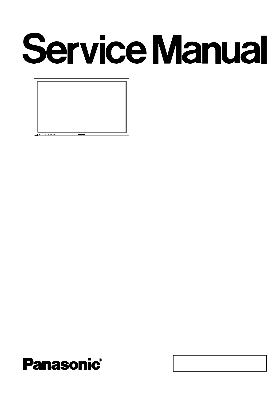
Progressive Wide Plasma Display
TH-37PW7BX
TH-37PW7EX
TH-37PWD7BK
TH-37PWD7EK
TH-37PWD7UY
TH-42PW7EX
TH-42PW7BX
TH-42PWD7BK
TH-42PWD7BS
Specifications
Power Source (UY Version)
Power Source (Except UY)
Power Consumption (UY Version)
Maximum
Stand-by condition
Power off condition
Power Consumption (Except UY)
Normal use
Stand-by condition
Power off condition
Plasma Display panel
Contrast Ratio
Screen size
(No. of pixels)
Operating condition
Temperatuer
Humidity
Applicable signals
Colour System
TH-42PWD7EK
TH-42PWD7ES
TH-42PWD7UY
GP7D Chassis
20 V AC, 50/60 Hz
20 - 240 V AC, 50/60Hz
25 W (37 inch)
ave OFF 0.8 W,SaveON0.5
.1 W
85 W (37 inch)
ave off 1.0 W, Saveon0.7
.3 W
rive method: ACtype16:9aspec
000:1
18 mm (W) × 461mm(H)
(37 inch)
08,960 (852 (W)
2 °F - 104 °F (0°C
0%-80%
TSC, PAL, PAL60,SECAM,ModifiedNTSC
H))[2,556
C)
atio
diagonal)
nch)
nch)
W) × 518 mm (H) × 1,056mm(diagonal)
(42 inch)
ots]
© 2004 Matsushita Electric Industrial Co., Ltd. All
rights reserved. Unauthorized copying and
distribution is a violation of law.
/
50i5
/
60p5
-
110k
-
120H
1
m
o
Y:1
0
1
/
c
0
/
n
/
B
)
0
×
2)0
)
R,G,B/0
H
/
1.0-
5
ComponentY:
1
m
:
PB/
CB:
±
PR/
CR:
±
0
B
9
%
T
×
2
×
2
1
×
610m
a
a
a
a
TH-37PW7BX
Scanning format 525(480) / 60i 60p,625(575)
25p 30p 24sF .... SMPTE274M, 1250 (1080) / 50i
PC signals VGAdisplay
VGA
SVGA, XGA, SXGA, UXGA.....(compressed)
Horizontal scanning frequency15
Vertical scanning frequency48
Connection terminals
AV (TH-37/42PWDUY) VIDEO IN / OUT (BNC)
S VIDEO IN (MINI DIN4PIN)
AUDIO IN (RCA PIN JACK×2)
COMPONENT / RGB (TH37/42PWDUY)
PC (HIGH-DENSITY D-SUB15PIN
SERIAL EXTERNAL CONTROLTERMINAL(D-SU
SPEAKERS (6 W) 16 W [8 W + 8 W] (10
Accessories Supplied
Remote Control Transmitter EUR646529
Batteries 2 × AA Size
Fixing bands (TMME203 or TMME187)
Ferrite core J0KF00000018 × 1, J0KG00000054
Dimensions ( W × H × D ) 920mm × 550 mm × 89mm(37inch)
Mass (Weight) (UY Version)
main unit only approx. 54.0 lbs (37 inch)
with speakers approx. 63.3 lbs (37 inch)
Mass (Weight) (Except UY)
main unit only approx. 24.0 kg net (37inch)
with speakers approx. 28.2 kg (37 inch)
Y/G(BNC)
PB
(BNC), PR / R (BNC
AUDIO IN (RCA PIN JACK
AUDIO IN (M3 JACK)
HD)
0p,750(720)
Hz
z
.0 Vp-p(75-oh
Vp-p(75-ohm), C: 0.286 Vp-p (75-ohm)
.5 Vrms(highimpedance)
.0 Vp-p
.7 Vp-p
.7 Vp-p(75ohm)
.5 Vrms(highimpedance)
D, VD
.0 Vp-p(75-oh
0.35 Vp-p(75-ohm)
0.35 Vp-p(75-ohm)
.5 Vrms(highimpedance)
PIN)RS-232CCOMPATIBLE
,020mm
pprox.63.9lbs(42 inch)
pprox.73.2lbs(42 inch)
pprox.28.5kgnet (42 inch)
pprox.32.7kg(42 inch)
0p, 1125 (1080) / 60i50i24p
r high impedance)
omposite (75-ohm)
on-composite (75-ohm)
.7 Vp-p (75-ohm)
.0 Vp-p (high impedance)
include sync)
m × 89 mm (42 inch)
Notes:
· Design and specifications are subject to change without notice.Mass and dimensions shown are approximate.
CONTENTS
Page Page
1 Applicable signals 5
2 Safety Precautions
2.1. General Guidelines
3 Prevention of Electro Static Discharge (ESD) to
Electrostatically Sensitive (ES) Devices
4 About lead free solder (PbF)
5 PCB Structure sheet of GP7D chassis
6
6
6 Service Hint
7 P.C.Board and Plasma panel replacement
7
7.1. Removal of the back cover
2
8
9
10
11
11
TH-37PW7BX
7.2. Removal of the Slot block 11
7.3. Removal of the J-Board
7.4. Removal of the HX-Board
7.5. Removal of the P-Board
7.6. Removal of the Z-Board
7.7. Removal of the D-Board
7.8. Removal of the PF-Board
7.9. Removal of the H3-Board
7.10. Removal of the SU-Board
7.11. Removal of the SD-Board
7.12. Removal of the SC-Board
7.13. Removal of the SS-Board
7.14. Removal of the C1-Board
7.15. Removal of the C2-Board
7.16. Removal of the Front frame (glass)
7.17. Removal of stand brackets
7.18. Replacement of the plasma panel
8 Location of Lead Wiring
9 Adjustment Procedure
9.1. Driver Set-up
9.2. Initialization Pulse Adjust
9.3. P.C.B. (Printed Circuit Board) exchange
9.4. Adjustment Volume Location
9.5. Test Point Location
10 Servi ce mode
10.1. CAT (computer Aided Test) mode
10.2. IIC mode structure (following items value is sample data.)
11 Alignment
11.1. PC/RGB panel white balance
11.2. HD/ 525i /525p /625i /625p panel white balance
12 Trouble shooting guide
12.1. Self Check
12.2. No Power
12.3. No Picture
12.4. Local screen failure
13 Option Setting
14 Circuit Board Layout
14.1. PF-Board (37 inch)
14.2. PF-Board (42 inch)
14.3. P-Board
14.4. HA-Board
14.5. HB-Board
14.6. HX-Board (37 inch)
14.7. HX-Board (42 inch)
14.8. J-Board (37 inch)
14.9. J-Board (42 inch)
14.10. D-Board
14.11. C1-Board (37 inch)
14.12. C1-Board (42 inch)
14.13. C2-Board (37 inch)
14.14. C2-Board (42 inch)
14.15. SC-Board
14.16. SU-Board (37 inch)
14.17. SU-Board (42 inch)
11
11
12
12
12
13
13
13
13
14
14.18. SD-Board (37 inch)
14.19. SD-Board (42 inch)
14.20. SS-Board
14.21. Z-Board
14.22. H3, S1 and V1-Board
15 Sche matic Diagr ams
15.1. Schematic Diagram Notes
15.2. Main Block Diagram
15.3. PF-Board Block Diagram
15.4. PF-Board Schematic Diagram (TH-37PW7/PWD7 series)
14
14
15.5. PF-Board Schematic Diagram (TH-42PW7/PWD7 series)
14
14
15
15
16
17
17
18
19
19
19
20
20
15.6. P-Board Block Diagram
15.7. P-Board (1 of 6) Schematic Diagram
15.8. P-Board (2 of 6) Schematic Diagram
15.9. P-Board (3 of 6) Schematic Diagram
15.10. P-Board (4 of 6) Schematic Diagram
15.11. P-Board (5 of 6) Schematic Diagram
15.12. P-Board (6 of 6) Schematic Diagram
15.13. HA-Board Block and Schematic Diagram
15.14. HB-Board Block Diagram
15.15. HB-Board (1 of 2) Schematic Diagram
15.16. HB-Board (2 of 2) Schematic Diagram
15.17. HX-Board Block Diagram
15.18. HX-Board Schematic Diagram
22
23
15.19. J-Board Block Diagram
15.20. J-Board (1 of 4) Schematic Diagram (TH-37PW7/PWD7
23
26
15.21. J-Board (2 of 4) Schematic Diagram (TH-37PW7/PWD7
28
28
15.22. J-Board (3 of 4) Schematic Diagram (TH-37PW7/PWD7
29
30
15.23. J-Board (4 of 4) Schematic Diagram (TH-37PW7/PWD7
30
31
15.24. J-Board (1 of 4) Schematic Diagram (TH-42PW7/PWD7
33
33
15.25. J-Board (2 of 4) Schematic Diagram (TH-42PW7/PWD7
35
37
15.26. J-Board (3 of 4) Schematic Diagram (TH-42PW7/PWD7
40
41
15.27. J-Board (4 of 4) Schematic Diagram (TH-42PW7/PWD7
42
43
44
46
48
50
51
52
53
54
57
15.28. D-Board Block Diagram
15.29. D-Board (1 of 12) Schematic Diagram
15.30. D-Board (2 of 12) Schematic Diagram
15.31. D-Board (3 of 12) Schematic Diagram
15.32. D-Board (4 of 12) Schematic Diagram
15.33. D-Board (5 of 12) Schematic Diagram
15.34. D-Board (6 of 12) Schematic Diagram
15.35. D-Board (7 of 12) Schematic Diagram
15.36. D-Board (8 of 12) Schematic Diagram
15.37. D-Board (9 of 12) Schematic Diagram
series)
series)
series)
series)
series)
series)
series)
series)
58
59
60
61
63
64
65
65
66
67
68
69
70
71
72
73
74
75
76
77
78
79
80
81
82
83
84
85
86
87
88
89
90
91
92
93
94
95
96
97
98
99
100
101
3
TH-37PW7BX
15.38. D-Board (10 of 12) Schematic Diagram 102
15.39. D-Board (11 of 12) Schematic Diagram
15.40. D-Board (12 of 12) Schematic Diagram
15.41. C1, C2 and V1-Board Block Diagram
103
104
105
15.42. C1-Board (1 of 2) Schematic Diagram (TH-37PW7/PWD7
series)
106
15.43. C1-Board (2 of 2) Schematic Diagram (TH-37PW7/PWD7
series)
107
15.44. C1-Board (1 of 2) Schematic Diagram (TH-42PW7/PWD7
series)
108
15.45. C1-Board (2 of 2) Schematic Diagram (TH-42PW7/PWD7
series)
109
15.46. C2-Board (1 of 2) and V1-Board Schematic Diagram (TH37PW7/PWD7 series)
110
15.47. C2-Board (2 of 2) Schematic Diagram (TH-37PW7/PWD7
series)
111
15.48. C2-Board (1 of 2) and V1-Board Schematic Diagram (TH42PW7/PWD7 series)
112
15.49. C2-Board (2 of 2) Schematic Diagram (TH-42PW7/PWD7
series)
15.50. SC-Board Block Diagram
15.51. SC-Board (1 of 2) Schematic Diagram
15.52. SC-Board (2 of 2) Schematic Diagram
15.53. SU-Board Block Diagram
113
114
115
116
117
15.54. SU-Board Schematic Diagram (TH-37PW7/PWD7 series)
15.55. SU-Board Schematic Diagram (TH-42PW7/PWD7 series)
15.56. SD-Board Block Diagram
15.57. SD-Board Schematic Diagram (TH-37PW7/PWD7 series)
15.58. SD-Board Schematic Diagram (TH-42PW7/PWD7 series)
15.59. SS and S1-Board Block Diagram
15.60. SS and S1-Board Schematic Diagram
15.61. Z and H3-Board Block Diagram
15.62. Z-Board (1 of 2) Schematic Diagram
15.63. Z-Board (2 of 2) and H3-Board Schematic Diagram
16 Parts Locatio n
17 Packing Exploded Views
17.1. Packing Exploded Views (1)
17.2. Packing Exploded Views (2)
17.3. Packing Exploded Views (3)
18 Mech ani ca l Replaceme nt Parts List
19 Repl acement Parts List
19.1. Replacement Parts List Notes
19.2. Electrical Replacement List
118
119
120
121
122
123
124
125
126
127
129
130
130
131
132
133
135
135
136
4
1 Applicable signals
TH-37PW7BX
5
TH-37PW7BX
2 Safety Precautions
2.1. General Guidelines
1. When servicing, observe the original lead dress. If a short circuit is found, replace all parts which have been overheated or
damaged by the short circuit.
2. After servicing, see to it that all the protective devices such as insulation barriers, insulation papers shields are properly
installed.
3. After servicing, make the following leakage current checks to prevent the customer from being exposed to shock hazards.
2.1.1. Leakage Current Cold Check
1. Unplug the AC cord and connect a jumper between the two
prongs on the plug.
2. Measure the resistance value, with an ohmmeter, between
the jumpered AC plug and each exposed metallic cabinet
part on the equipment such as screwheads, connectors,
control shafts, etc. When the exposed metallic part has a
return path to the chassis, the reading should be between
1MW and 5.2MW.
When the exposed metal does not have a return path to
the chassis, the reading must be
.
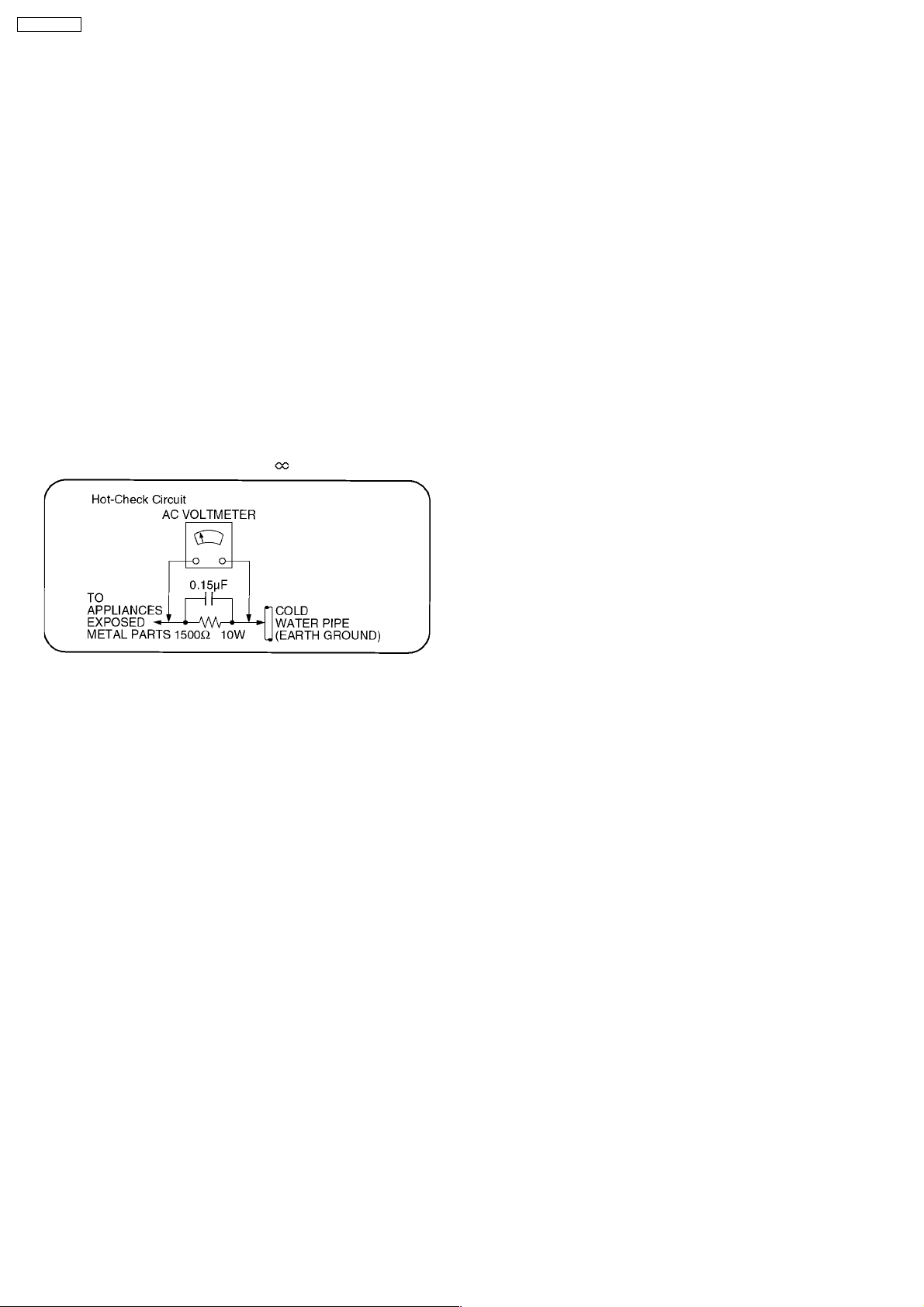
Figure 1
2.1.2. Leakage Current Hot Check (See
Figure 1.)
1. Plug the AC cord directly into the AC outlet. Do not use an
isolation transformer for this check.
2. Connect a 1.5kW, 10 watts resistor, in parallel with a 0.15µF
capacitors, between each exposed metallic part on the set
and a good earth ground such as a water pipe, as shown in
Figure 1.
3. Use an AC voltmeter, with 1000 ohms/volt or more
sensitivity, to measure the potential across the resistor.
4. Check each exposed metallic part, and measure the
voltage at each point.
5. Reverse the ACplugintheAC outlet andrepeat each of the
above measurements.
6. The potential at any point should not exceed 0.75 volts
RMS. A leakage current tester (Simpson Model 229 or
equivalent) may be used to make the hot checks, leakage
current must not exceed 1/2 milliamp. In case a
measurement is outside of the limits specified, there is a
possibility of a shock hazard, and the equipment should be
repaired and rechecked before it is returned to the
customer.
6
TH-37PW7BX
3 Prevention of Electro Static Discharge (ESD) to
Electrostatically Sensitive (ES) Devices
Some semiconductor (solid state) devices can be damaged easily by static electricity. Such components commonly are called
Electrostatically Sensitive (ES) Devices. Examples of typical ES devices are integrated circuits and some field-effect transistors and
semiconductor "chip" components. The following techniques should be used to help reduce the incidence of component damage
caused by electro static discharge (ESD).
1. Immediately before handling any semiconductor component or semiconductor-equipped assembly, drain off any ESD on your
body by touching a known earth ground. Alternatively, obtain and wear a commercially available discharging ESD wrist strap,
which should be removed for potential shock reasons prior to applying power to the unit under test.
2. After removing an electrical assembly equipped with ES devices, place the assembly on a conductive surface such as alminum
foil, to prevent electrostatic charge buildup or exposure of the assembly.
3. Use only a grounded-tip soldering iron to solder or unsolder ES devices.
4. Use only an anti-static solder removal device. Some solder removal devices not classified as "anti-static (ESD protected)" can
generate electrical charge sufficient to damage ES devices.
5. Do not use freon-propelled chemicals. These can generate electrical charges sufficient to damage ES devices.
6. Do not remove a replacement ES device from its protective package until immediately before you are ready to install it. (Most
replacement ES devices are packaged with leads electrically shorted together by conductive foam, alminum foil or comparable
conductive material).
7. Immediately before removing the protective material from the leads of a replacement ES device, touch the protective material
to the chassis or circuit assembly into which the device will be installed.
Caution
Be sure no power is applied to the chassis or circuit, and observe all other safety precautions.
8. Minimize bodily motions when handling unpackaged replacement ES devices. (Otherwise hamless motion such asthe brushing
together of your clothes fabric or the lifting of your foot from a carpeted floor can generate static electricity (ESD) sufficient to
damage an ES device).
7
TH-37PW7BX
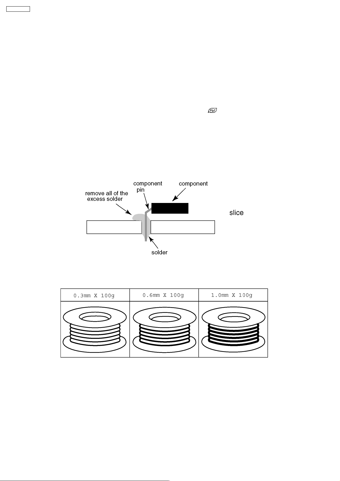
4 About lead free solder (PbF)
Note: Lead is listed as (Pb) in the periodic table of elements.
In the information below, Pb will refer to Lead solder, and PbF will refer to Lead Free Solder.
The Lead Free Solder used in our manufacturing process and discussed below is (Sn+Ag+Cu).
That is Tin (Sn), Silver (Ag) and Copper (Cu) although other types are available.
This model uses Pb Free solder in it’s manufacture due to environmental conservation issues. For service and repair work, we’d
suggest the use of Pb free solder as well, although Pb solder may be used.
PCBs manufactured using lead free solder will have the PbF within a leaf Symbol
Caution
· Pb free solder has a higher melting point than standard solder. Typically the melting point is 50 ~ 70 °F (30~40 °C) higher.
Please use a high temperature soldering iron and set it to 700 ± 20 °F (370 ± 10 °C).
· Pb free solder will tend to splash when heated too high (about 1100 °F or 600 °C).
If you must use Pb solder, please completely remove all of the Pb free solder on the pins or solder area before applying Pb
solder. If this is not practical, be sure to heat the Pb free solder until it melts, before applying Pb solder.
· After applying PbF solder to double layered boards, please check the component side for excess solder which may flow onto
the opposite side. (see figure below)
Suggested Pb free solder
There are several kinds of Pb free solder available for purchase. This product uses Sn+Ag+Cu (tin, silver, copper) solder.
However, Sn+Cu (tin, copper), Sn+Zn+Bi (tin, zinc, bismuth) solder can also be used.
stamped on the back of PCB.
8
5 PCB Structure sheet of GP7D chassis
Board Name Function Remarks
D Digital Signal Processor 1
J Slot Interface & SYNC processor 1
Z Audio out, DC-DC converter
SS Sustain Out 1
SC Scan out 1
SU Sustain connection (Upper) 1
SD Sustain connection (Lower) 1
C1 Data Drive (Lower Right)
C2 Data Drive (Lower Left)
H3 Speaker terminal
S1 Power switch
SS2 Sustain connection (Upper)
SS3 Sustain connection (Lower)
V1 Front SW. & Remote receiver
PF Line filter
P Power supply 1
HX PC_type_Input terminal
HB BNC Composite/Component Video 2
HA BNC Component Video 2
Remarks
1. Recommend PCB´s for initial service for GP7D chassis.
2. For System model except BK, BS, EK, ES model
TH-37PW7BX
9
TH-37PW7BX
6 Service Hint
Service position for HB-Board, HA-Board and TY-42TM6
Note:
Extension cable kit for Slot Board is supplied as service fixtures and tools.
(Part No. TZSC07040)
10
7 P.C.Board and Plasma panel replacement
TH-37PW7BX
Prior to the replacement, place the unit on the pedestal
stand remove the front frame.
7.1. Removal of the back cover
a. Unscrew the screws (×16 ,×6 ,×4 ) and remove the
back cover.
7.2. Removal of the Slot block
a. Unscrew the couplers (J1, J3, J5, J6, J8, J10).
b. Unscrew the screws (×4) and remove the slot block.
7.3. Removal of the J-Board
a. Unscrew the screws (×7) and remote the J-Board.
7.4. Removal of the HX-Board
a. Unscrew the screws (×6) and remove the slot case.
b. Unscrew the screws (×4).
c. Unscrew the screws (×2) and remove the HX-Board.
11
TH-37PW7BX
7.5. Removal of the P-Board
a. Remove the couplers (P2, P5, P7, P9, P10, P11, P12, P23,
P25, P27).
b. Unscrew the screws (×5) and remove the P-Board.
7.6. Removal of the Z-Board
7.7. Removal of the D-Board
a. Disconnect the couplers (D1, D3, D5, D25, D27) and the
flexible cables (D31, D32).
b. Remove the shield cuse.
c. Unscrew the screws (×6) and remove the D -Board.
a. Remove the couplers (Z5, Z6, Z7, Z8).
b. Unscrew the screws (×4
theZ-BoardBracket.
c. Unscrew the screws (×4
) and remove the Z-Board with
) and remove the Z-Board.
12
TH-37PW7BX
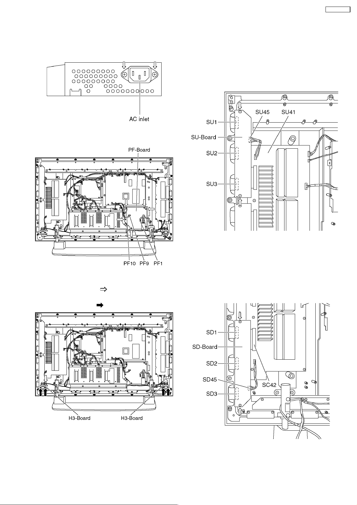
7.8. Removal of the PF-Board
a. Remove the coupler (PF1).
b. Unscrew the screws (×2) and remove the AC inlet.
c. Remove the couplers (PF9, PF10).
d. Unscrew the screws (×4), and remove the PF-Board.
7.10. Removal of the SU-Board
a. Unscrew the screws (×2).
b. Slide the SU-Board to the left and disconnect from the
couplers (SC41) on the SC-Board.
c. Remove the coupler (SU45).
d. Remove the flexible cables (SU1, SU2, SU3) connected to
the SU-Board, and remove the SU-Board.
7.9. Removal of the H3-Board
a. Unscrew the screws (×2 ), and remove the H3-Board
with the Bracket.
b. Unscrew the screws (×4
), and remove the H3-Board.
7.11. Removal of the SD-Board
a. Unscrew the screws (×2).
b. Slide the SD-Board to the left and disconnect from the
couplers (SC42) on the SC-Board.
c. Remove the coupler (SD46).
d. Remove the flexible cables (SD1, SD2, SD3) connected to
the SD-Board, and remove the SD-Board.
13
TH-37PW7BX
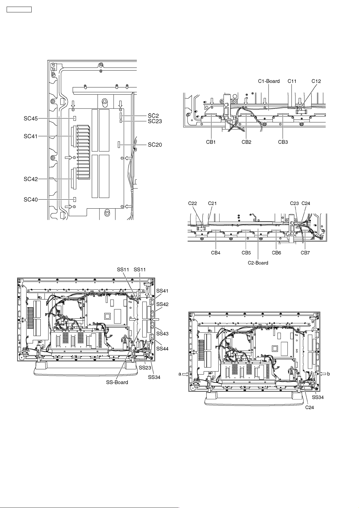
7.12. Removal of the SC-Board
a. Remove the couplers (SC2, SC20, SC23, SC45, SC46).
Unscrew the screws (×6) and remove the SC-Board.
7.14. Removal of the C1-Board
a. Remove the flexible cables (CB1, CB2, CB3).
b. Remove the flexible cables (C11, C12) release the speaker
cables from the clampers (×2) on the C1-Board.
c. Unscrew the screws (×4), and remove the C1-Board.
7.15. Removal of the C2-Board
a. Remove the cables (CB4, CB5, CB6, CB7).
b. Remove the couplers (C23, C24), a flexible cable (C21) and
release the speaker cables from the clamper on the C2-Board.
c. Unscrew the screws (×4), and remove the C2-Board.
7.13. Removal of the SS-Board
a. Remove the couplers (SS11, SS12, SS23, SS34).
b. Remove the flexible cables (SS41, SS42, SS43, SS44).
c. Unscrew the screws (×6), and remove the SS-Board.
7.16. Removal of the Front frame
(glass)
a. Remove the screws (×2) fasten on the panel and remove the
front panel.
14
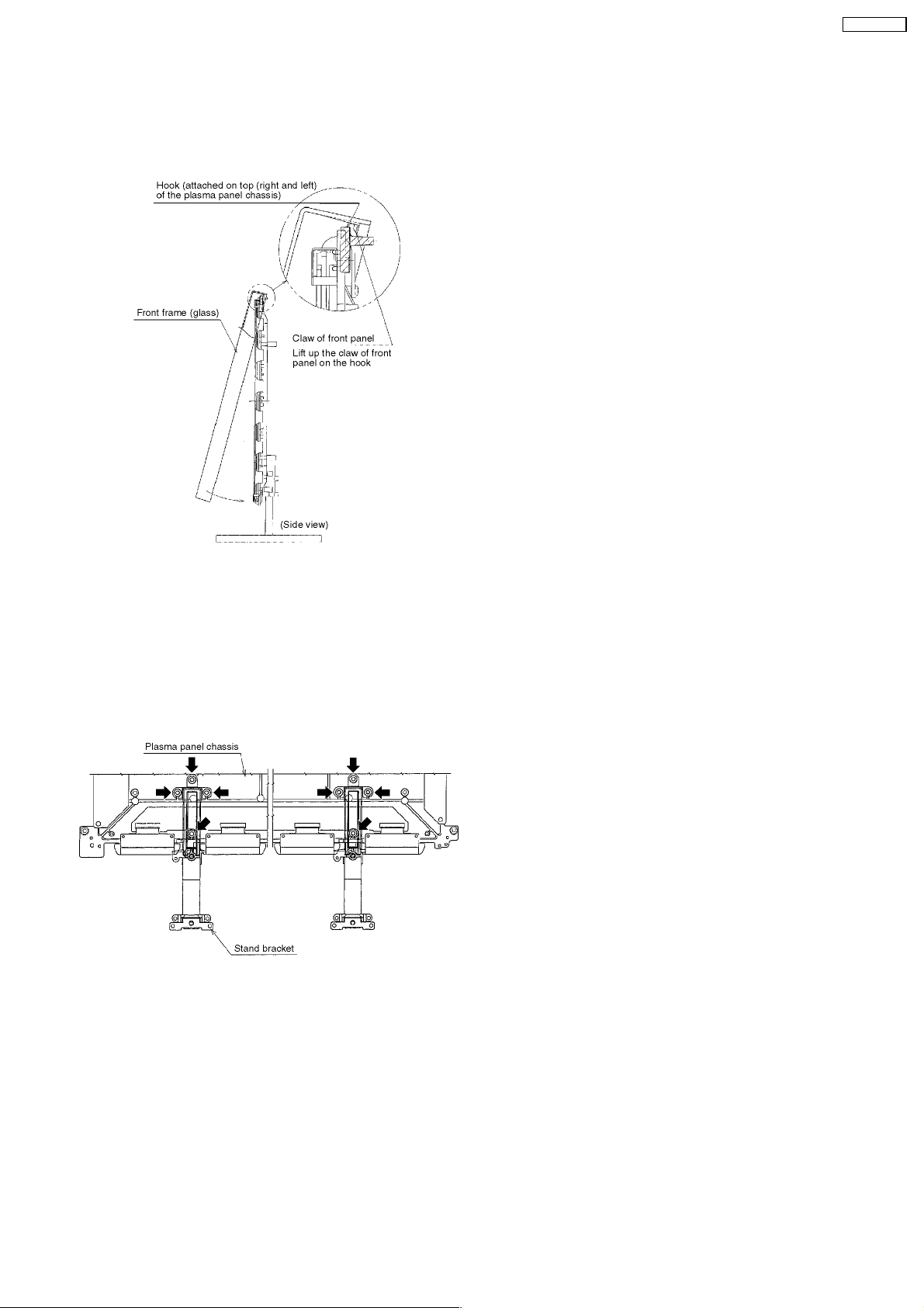
b. Release all cables from the clamper on the bracket of the
front frame.
c. For leaving the plasma panel from the front frame, pull the
bottom of the front frame to forward, lift, and remove.
TH-37PW7BX
7.18. Replacement of the plasma
panel
a. Place the new plasma panel (finished) on the flat surface of
the table (covered by a soft cloth), with the plasma panel
surface facing downward.
b. Fit the stand brackets (left, right.) fast 4 screws each on the
new plasma panel.
c. Place the plasma panel section on the servicing stand.
d. Attach the front frame each P.C.Board and so on, to the new
plasma panel.
* When fitting the front frame, be careful not to allow any
debris, dust or handling residues to remain between the
front glass and plasma panel.
7.17. Removal of stand brackets
a. Remove the plasma panel section from the servicing stand
and lay on a table (covered), with the plasma panel surface
facing downward.
Spread a soft cloth for protection, to prevent panel surface from
scratching.
b. Remove the stand bracket (left, right) fastening screws (×4
each) and remove the stand brackets (left, right).
15
TH-37PW7BX
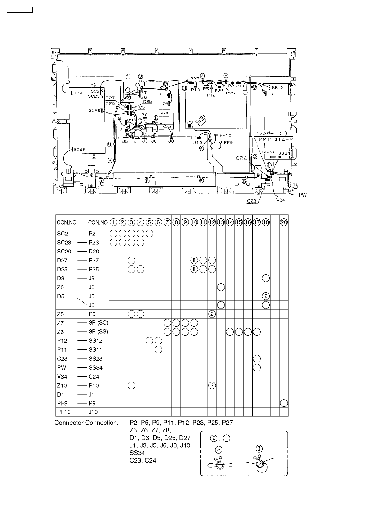
8 Location of Lead Wiring
16
9 Adjustment Procedure
TH-37PW7BX
9.1. Driver Set-up
9.1.1. Item / Preparation
1. Input an APL 100 % white signal.
2. Set the picture controls: Picture mode: Normal
White balance: Normal
Aspect: 16:9
9.1.2. Adjustments
Adjust driver section voltages referring the panel data on the
panel data label.
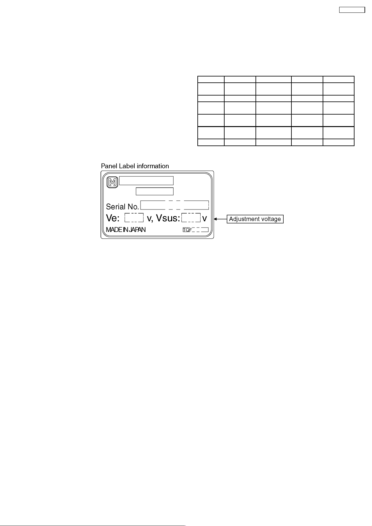
Name Test Point Voltage Volume Remarks
Vsus TPVSUS
(SS)
Ve TPVE (SS) 156V ± 1V VR6074 (SS)
Vset TPVSET
(SC)
Vad TPVAD (SC) -90V ± 1V VR6477
Vscn TPVSCN
(SC)
Vda TPVDA (SS) 67V ± 1V R665 (P)
*See the Panel label.
174V ± 1V R628 (P)
232V ± 5V ---
(SC)
Vad*+120V ±2V---
17
TH-37PW7BX
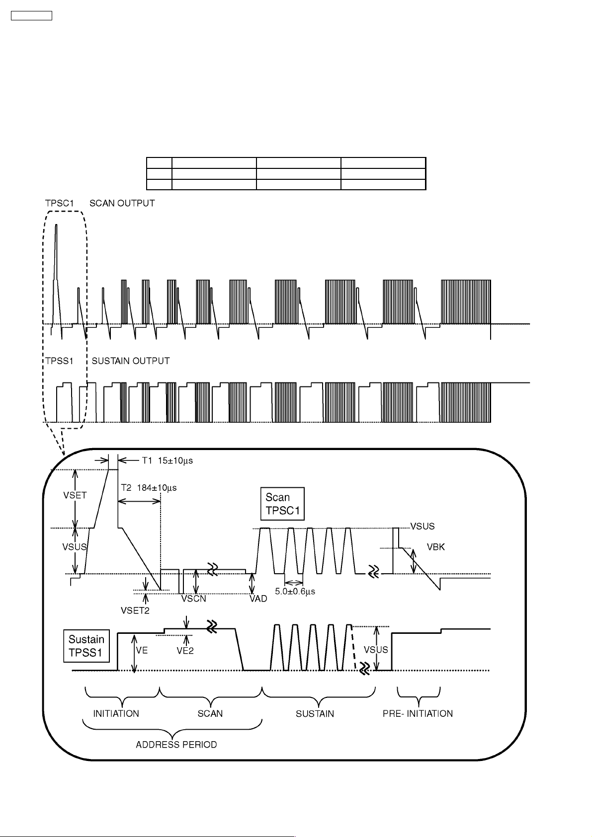
9.2. Initialization Pulse Adjust
1. Input the Cross hatch signal to plasma video input.
2. Set the picture controls as follows.
· Picture mode: Normal
· White balance: Cool
3. Connect OSC: lloscope to TPSCI and adjust R6523 for 15±10µ Sec.
4. Connect OSC: lloscope to TPSCI and adjust R6557 for 184±10µ Sec.
Test point Volume Level
T1 TPSC1 (SC) R6523 (SC) 15 ± 10µ Sec
T2 TPSS1 (SS) R6557 (SC) 184 ± 10µ Sec
18
9.3. P.C.B. (Printed Circuit Board) exchange
9.3.1. Caution
1. To remove P.C.B. , wait 1 minute after power was off for discharge from electrolysis capacitors.
9.3.2. Quick adjustment after P.C.B. exchange
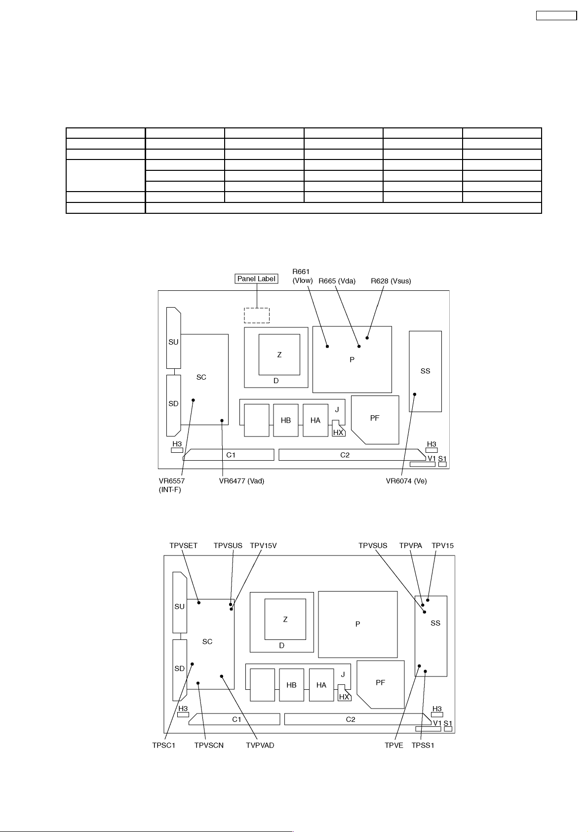
P.C.B. Name Test Point Voltage Volume Remarks
P Board Vsus TPVSUS (SS) 174V ± 1V R628 (P)
Vda TPVDA (SS) 67V ± 1V R665 (P)
SC Board Vad TPVAD (SC) -90V ± 1V VR6477 (SC)
Vset TPVSET (SC) 232V ± 5V --Vscn TPVSCN (SC) Vad + 120 ± 2V ---
SS Board Ve TPVE (SS) 156V ± 1V VR6074 (SS)
D, J Board White blance, Pedestal and Sub brightness for NTSC, PAL, HD, PC and 625i signals
*See the Panel label.
9.4. Adjustment Volume Location
TH-37PW7BX
9.5. Test Point Location
19
TH-37PW7BX
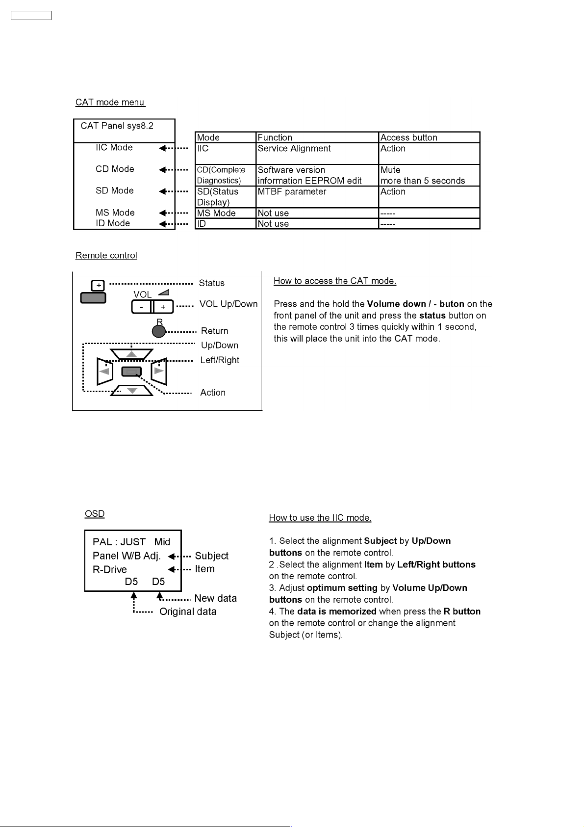
10 Service mode
10.1. CAT (computer Aided Test) mode
To exit the CAT mode, access the ID mode and switch off the main power.
10.1.1. IIC mode
Select the IIC mode by Up/Down button on the remote control at the front page of CAT mode then press the Action button on
the remote control.
Subject and item are mentioned on page 14.
To exit the IIC mode, press the R button on the remote control.
20
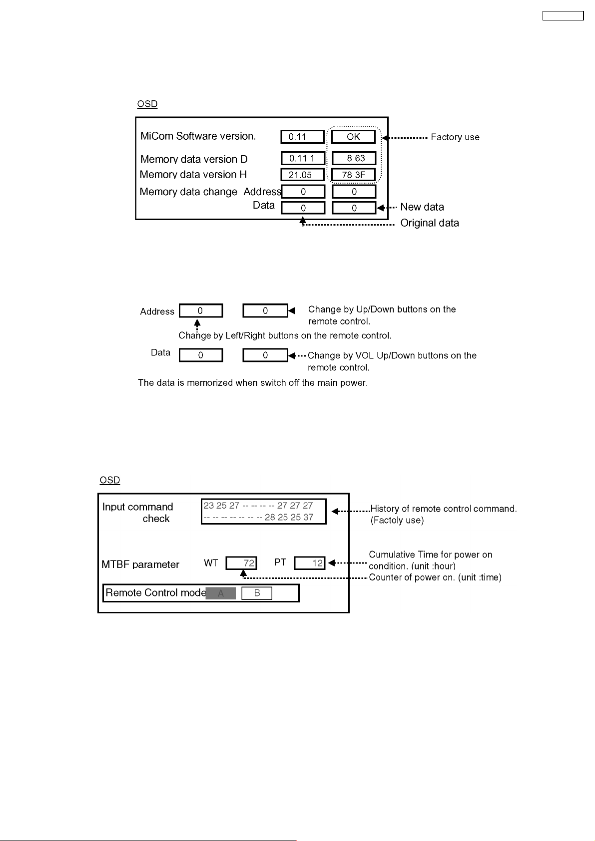
TH-37PW7BX
10.1.2. CD mode
Select the CD mode by Up/Down button on the remote control at the front page of CAT mode then press the Mute button on the
remote control more than 5 sec.
Micom software version (IC9354), this version can be upgrade by
1. replace of new version IC
2. Loading the new version software from loader tool, TZSC07036.
Memory data change
To exit the CD mode, press the R button on the remote control.
10.1.3. SD mode
Select the SD mode by Up/Down button on the remote control at the front page of CAT mode then press the Action button on the
remote control.
To exit the SD mode, press the R button on the remote control.
21
TH-37PW7BX
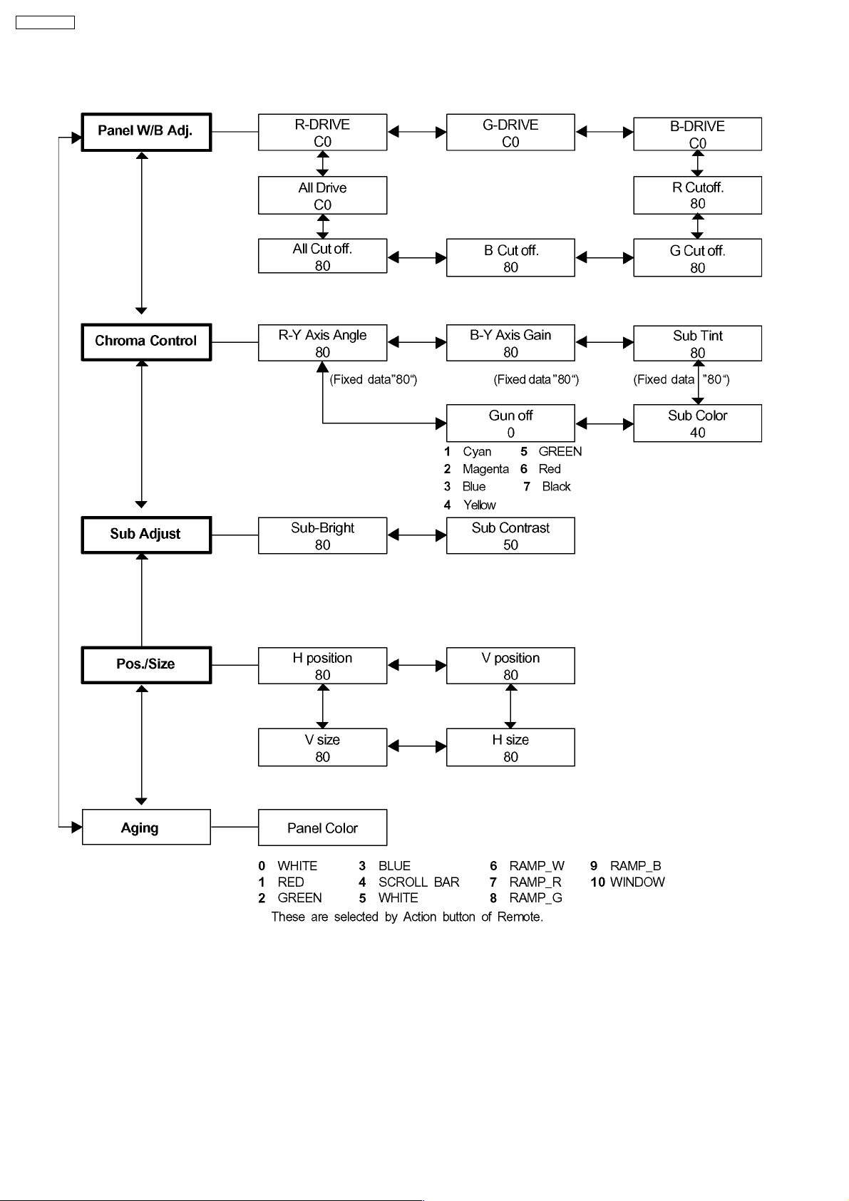
10.2. IIC mode structure (following items value is sample data.)
22
11 Alignment
11.1. PC/RGB panel white balance
INPUT Alignment menu ProcedureEquipment Setting
TH-37PW7BX
1 PC Color Picture:
Gray Scale Analyzer Normal
Pattern White balance:
Aspect:
High light 75%
Low light 15%
1) Set G cut off to " 80 ".
Cool
16:9
2)Find 75% of white area by color sensor.
PANEL W/B
G Drive 3) Set G Drive to " E8 ".
PANEL W/B
B Drive 4) Adjust B and R Drive to set color temperature
R Drive as shown Fig.-03.
PANEL W/B
R,G,B Drive 5) Increase same steps of R, G and B Drive to set
R,G,B Drive largest level of 3 color drive to "FC".
PANEL W/B
R,G,B cut off
Color Temp. x y
Cool(Hi) 0.276 0.276
Normal(Mid) 0.288 0.296
Warm(Low) 0.313 0.329
Fig. -03
2 Picture: 1) Change white balance to "Normal".
Normal PANEL W/B
White balance: R,G,B cut off 2) Repeat procedure 1) to 5) of Cool mode.
Normal PANEL W/B
Aspect: R,G,B Drive
16:9
3 Picture: 1) Change white balance to "Warm".
Normal PANEL W/B
White balance: R,G,B cut off 2) Repeat procedure 1) to 5) of Cool mode.
Warm PANEL W/B
Aspect: R,G,B Drive
16:9
4 Picture: Picture Menu 1) Change color templature to "Cool".
Normal Sub Adjust
White balance: Sub Bright
Cool
Aspect:
16:9
23
TH-37PW7BX
INPUT Alignment menu ProcedureEquipment Setting
5 Picture: 1) Write down each color temaparature of R,G,B drive and
Normal Cut off data as follows.
Aspect:
16:9
White
RGB
Gray Scale
Pattern
White balance:
Cool R Drive
Normal G Drive
Warm B Drive
Balance Cool Normal Warm
R Cut off
G Cut off
B Cut off
2) Input RGB signal.
High light 75%
Low light 15% 3) Copy PC R,G,B drive and cut off data of each white
balance mode to RGB position.
6 Picture: 1) Write down each color temaparature of R,G,B drive and
Normal Cut off data as follows.
Aspect:
16:9
White
DVI
Gray Scale
Pattern
White balance:
Cool R Drive
Normal G Drive
Warm B Drive
Balance Cool Normal Warm
R Cut off
G Cut off
B Cut off
2) Input NTSC signal.
High light 75%
Low light 15% 3) Copy PC R,G,B drive and cut off data of each white
balance mode to DVI position.
24
INPUT Alignment menu ProcedureEquipment Setting
7 Picture: 1) Write down each color temaparature of R,G,B drive and
Normal Cut off data as follows.
Aspect:
16:9
White
RGB
Gray Scale
Pattern
White balance:
Cool R Drive
Normal G Drive
Warm B Drive
Balance Cool Normal Warm
R Cut off
G Cut off
B Cut off
2) Input PAL signal.
High light 75%
Low light 15% 3) Copy PC R,G,B drive and cut off data of each white
balance mode to RGB position.
TH-37PW7BX
8 Picture: 1) Write down each color temaparature of R,G,B drive and
Normal Cut off data as follows.
Aspect:
16:9
White
DVI
Gray Scale
Pattern
White balance:
Cool R Drive
Normal G Drive
Warm B Drive
Balance Cool Normal Warm
R Cut off
G Cut off
B Cut off
2) Input DVI signal.
High light 75%
Low light 15% 3) Copy PC R,G,B drive and cut off data of each white
balance mode to DVI position.
25
TH-37PW7BX
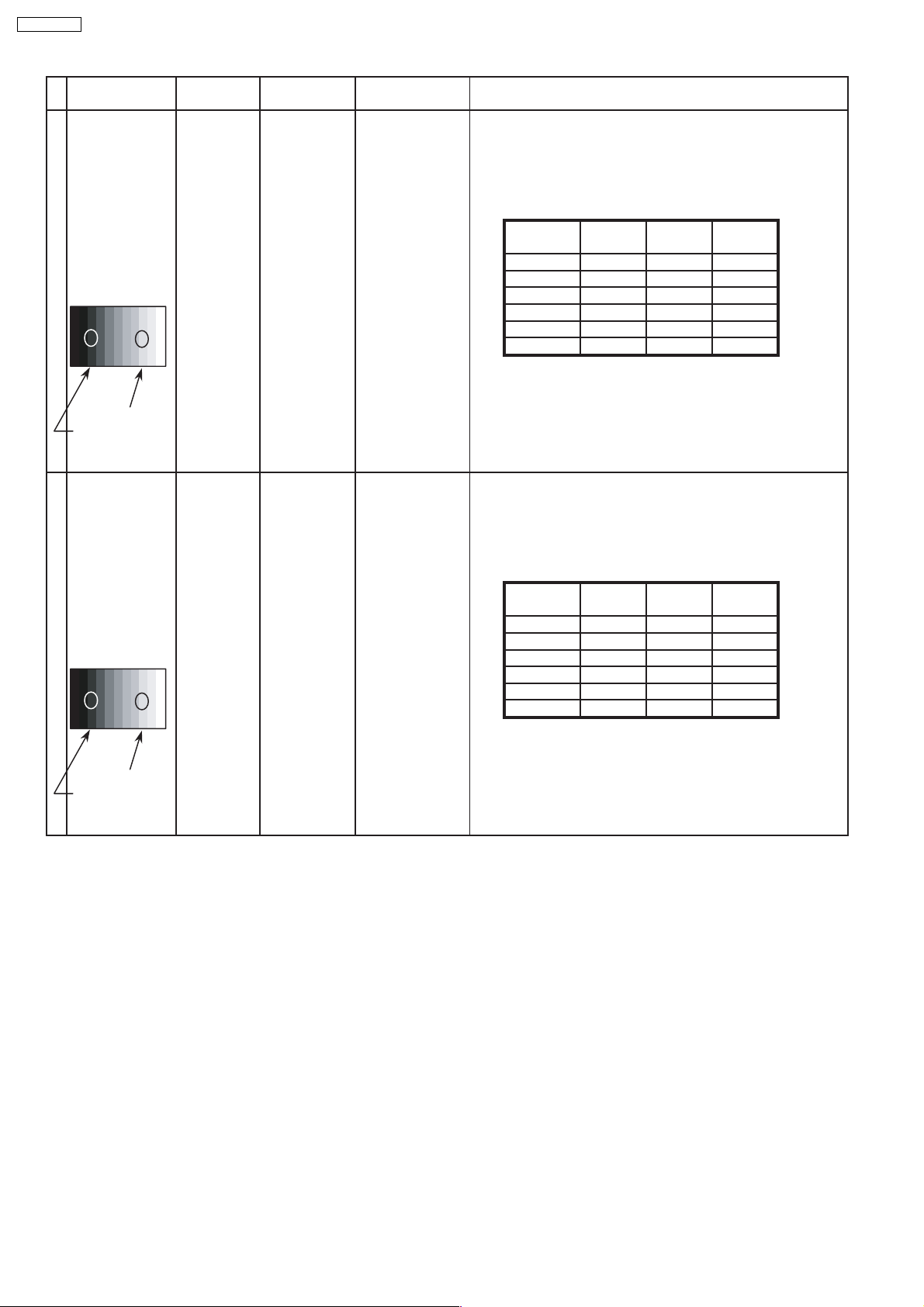
11.2. HD/ 525i /525p /625i /625p panel white balance
INPUT Alignment menu ProcedureEquipment Setting
1HD(720i or 1080i) Color Picture:
Gray Scale Analyzer Normal
Pattern
High light 75%
Low light 15%
White balance:
Cool
Aspect: PANEL W/B
16:9 G cut off 1) Set G cut off to " 80 ".
PANEL W/B
B cut off
R cut off
Sub Adjust
Sub Bright
2)Find 75% of white area by color sensor.
PANEL W/B
G Drive 3) Set G Drive to " E8 ".
PANEL W/B
B Drive 4) Adjust B and R Drive to set color temperature
R Drive as shown Fig.-04.
PANEL W/B
R,G,B Drive 5) Increase same steps of R, G and B Drive to set
R,G,B Drive largest level of 3 color drive to "FC".
PANEL W/B
R,G,B cut off
Color Temp. x y
Cool(Hi) 0.276 0.276
Normal(Mid) 0.288 0.296
Warm(Low) 0.313 0.329
Fig. -04
2 Picture: 1) Change white balance to "Normal".
Normal PANEL W/B
White balance: R,G,B cut off 2) Repeat procedure 1) to 5) of Cool mode.
Normal PANEL W/B
Aspect: R,G,B Drive
16:9
3 Picture: 1) Change white balance to "Warm".
Normal PANEL W/B
White balance: R,G,B cut off 2) Repeat procedure 1) to 5) of Cool mode.
Warm PANEL W/B
Aspect: R,G,B Drive
16:9
4 Picture: Picture Menu 1) Change color templature to "Cool".
Normal Sub Adjust
White balance: Sub Bright
Cool
Aspect:
16:9
26
INPUT Alignment menu ProcedureEquipment Setting
5 Picture: 1) Write down each color temaparature of R,G,B drive and
Normal Cut off data as follows.
Aspect:
16:9
White
RGB
Gray Scale
Pattern
White balance:
Cool R Drive
Normal G Drive
Warm B Drive
Balance Cool Normal Warm
R Cut off
G Cut off
B Cut off
2)Change input signal to 525i and 525p.
High light 75%
Low light 15% 3) Copy HD drive and cut off data of each white
balance mode to each signals position.
6 Picture: 1) Write down each color temaparature of R,G,B drive and
Normal Cut off data as follows.
Aspect:
16:9
White
RGB
Gray Scale
Pattern
White balance:
Cool R Drive
Normal G Drive
Warm B Drive
Balance Cool Normal Warm
R Cut off
G Cut off
B Cut off
TH-37PW7BX
2)Change input signal to 525p and 625i.
High light 75%
Low light 15% 3) Copy HD drive and cut off data of each white
balance mode to each signals position.
7 Picture: 1) Write down each color temaparature of R,G,B drive and
Normal Cut off data as follows.
Aspect:
16:9
White
RGB
Gray Scale
Pattern
White balance:
Cool R Drive
Normal G Drive
Warm B Drive
Balance Cool Normal Warm
R Cut off
G Cut off
B Cut off
2)Change input signal to 625i and 625p.
High light 75%
Low light 15% 3) Copy HD drive and cut off data of each white
balance mode to each signals position.
27
TH-37PW7BX
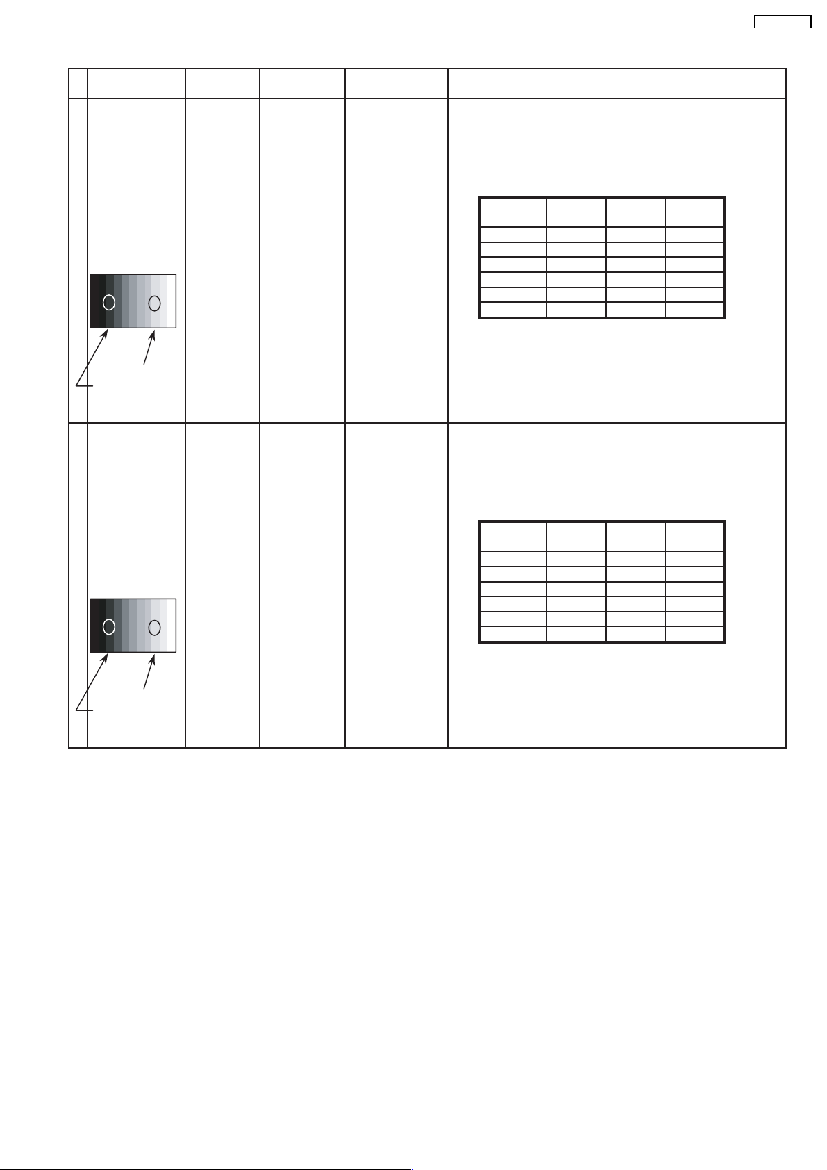
12 Trouble shooting guide
12.1. Self Check
12.1.1. Display Indication
1. Self-check is used to automatically check the bus line
controlled circuit of the Plasma display.
2. To get into the Self-check mode, press the volume down
button on the customer controls at the front of the set, at the
same time pressing the OFF-TIMER button on the remote
control, and the screen will show :-
If the CCU ports have been checked and found to be incorrect
Or not located then " - - " will appear in place of " OK "
12.1.2. Power LED Blinking timing chart
1. Subject
Information of LED Flashing timing chart.
2. Contents
When an abnormality has occurred the unit, the protection circuit operates and reset to the stand by mode. At this time, the
defective block can be identified by the number of blinkes of the Power LED on the front panel of the unit.
3. Remarks
Above Fan function is operated during the fans are installed.
28
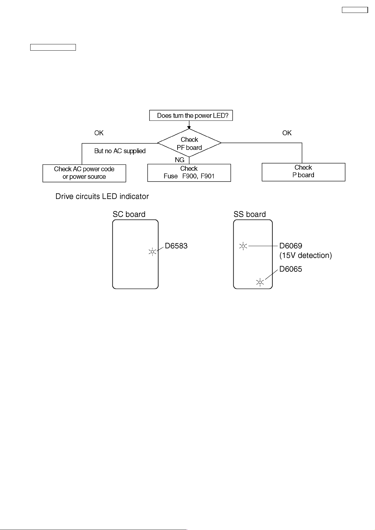
12.2. No Power
First check point
There are following 3 states of No Power indication by power LED.
1. No lit
2. Green is lit then turns red blinking a few seconds later.
3. Only red is lit.
1. No lit
TH-37PW7BX
29
TH-37PW7BX
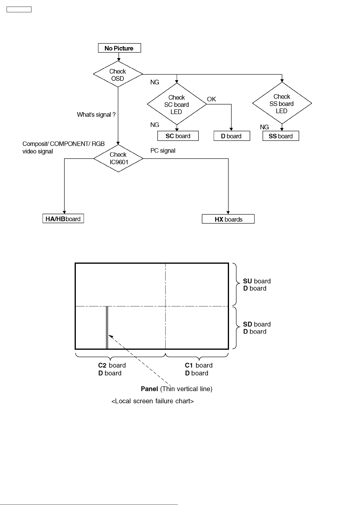
12.3. No Picture
12.4. Local screen failure
Plasma display may have local area failure on the screen. Fig - 1 is the possible defect P.C.B. for each local area.
Fig - 1
30
 Loading...