

Panasonic TH 42PA20U Service Manual
Panasonic Services Company
National Training
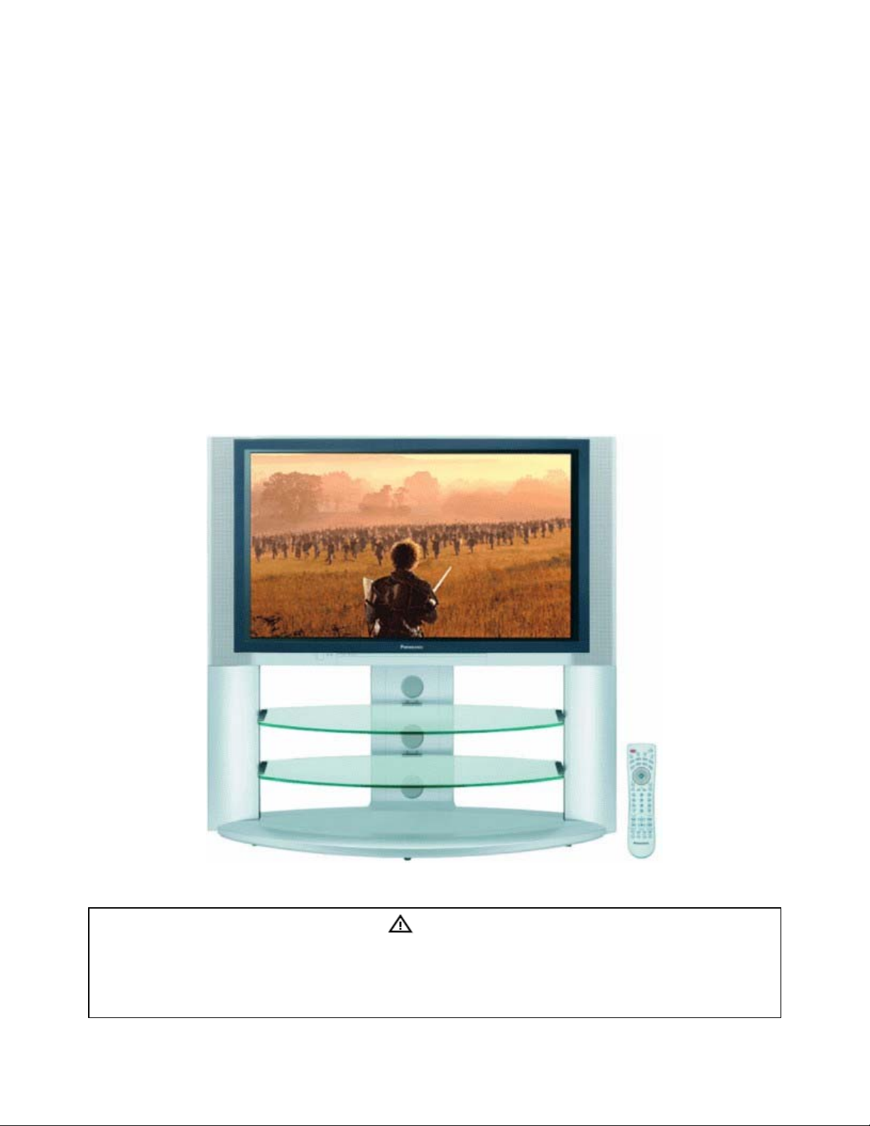
TH-42PX20U/TH-50PX20U
TH-42PA20U/TH-37PA20U
Plasma Display Panel
GP6D Chassis
Update Information
This service information is designed for experienced repair technicians only and is not designed for use by the general public. It does
not contain warnings or cautions to advise non-technical individuals of potential dangers in attempting to service a product. Products
powered by electricity should be serviced or repaired only by experienced professional technicians. Any attempt to service or repair
the product or products dealt with in this service information by anyone else could result in serious injury or death.
1
Warning

2

Table of contents
Objective..............................................................................................................5
Model Line Up .....................................................................................................7
Performance Comparison..................................................................................8
SD Models.........................................................................................................8
HD Models ........................................................................................................8
Specifications......................................................................................................9
SD Models.........................................................................................................9
HD Models ........................................................................................................9
New Features and Circuit Improvements .......................................................10
42” SD PCB Board Layout Diagram................................................................11
Board Comparison Chart .................................................................................12
Video Signal Block Diagram ............................................................................13
Video Signal Path Explanation ........................................................................15
NTSC \ 480i Video Signal Path .......................................................................15
DVI Input.........................................................................................................17
DVI RGB to YUV Conversion..........................................................................18
Digital Processor.............................................................................................19
Main Picture ....................................................................................................19
RGB Amplifier..................................................................................................21
RGB/PC Select................................................................................................22
D Board Outline...............................................................................................23
Sync Signal Process .......................................................................................24
SC Board Explanation......................................................................................25
SS Board Explanation ......................................................................................28
Power Supplies (GP6D Chassis) .....................................................................31
Standby power supply.....................................................................................31
VSUS High Voltage Source.............................................................................32
Main Power Supply .........................................................................................34
VDA and other Voltage Sources......................................................................35
Protection Circuits............................................................................................37
System Control Circuit.....................................................................................39
Panel Operations.............................................................................................39
TV Operations.................................................................................................40
Diagnostic Procedures.....................................................................................41
Diagnostic Flow Charts....................................................................................42
No Power ........................................................................................................42
No Picture Flowchart 1....................................................................................43
No picture Flowchart 2 ....................................................................................44
Dark picture Flowchart ....................................................................................45
Local screen failure..........................................................................................46
Service Hints...................................................................................................47
Adjustments......................................................................................................52
3

+B Set-up........................................................................................................52
Confirmation....................................................................................................52
Driver Set-up...................................................................................................53
Panel Label information...................................................................................53
Initialization Pulse Adjust.................................................................................54
P.C.B. (Printed Circuit Board) exchange procedure........................................55
Adjustment Volume Locations.........................................................................55
Test Point locations.........................................................................................56
Serviceman mode (Electronic Controls).........................................................56
Serviceman mode (Electronic Controls).........................................................57
CAT (computer aided test) Mode ....................................................................58
I2C Mode .........................................................................................................59
I2C Menu Structure..........................................................................................60
CD mode.........................................................................................................61
SD Mode ......................................................................................................... 62
Alignment Procedures......................................................................................63
Pedestal Setting..............................................................................................63
NTSC White Balance Adjustment....................................................................64
HD Panel White Balance Adjustment..............................................................65
Sub Brightness Setting....................................................................................66
Hotel Mode Operation.....................................................................................67
Service Contact Information............................................................................70
4

Objective
The information provided in this document is designed to assist the technician in
determining the defective printed circuit board. The troubleshooting flow charts,
signal path charts and connector information should provide enough detail to the
technician for the accurate repair of the product. Alignment and adjustment
procedures are also included in this document.
The Block diagrams and the schematic drawings reference the model TH42PHD5, TH-42PX20U and TH-42PA20U but the technology is consistent with
any GPH5D and GP6D series Plasma display panels.
5

6
Model Line Up
TH-50PX20U
50-inch (127 cm) HD Version
2 Component Video Inputs
3 Composite Video Inputs
3 S-Video Inputs
1 HDMI input
Scalable PIP (1/4 to 1/16)
PC / SD Card Inputs
Integrated Speaker System
BBE sound
1080i / 480p capable
720p (PC input only)
TH-42PX20U
42-inch (106cm) HD Version
2 Component Video Inputs
3 Composite Video Inputs
3 S-Video Inputs
1 HDMI input
Scalable PIP (1/4 to 1/16)
PC / SD Card Inputs
Integrated Speaker System
BBE sound
1080i / 480p capable
720p (PC input only)
TH-42PA20U
42-inch (106 cm) SD Version
2 Component Video Inputs
3 Composite Video Inputs
3 S-Video Inputs
1 DVI input
Scalable PIP (1/4 to 1/16)
Integrated Speaker System
BBE sound
1080i / 480p capable
TH-37PA20U
37-inch (94cm) SD Version
2 Component Video Inputs
3 Composite Video Inputs
3 S-Video Inputs
1 DVI input
Scalable PIP (1/4 to 1/16)
Integrated Speaker System
BBE sound
1080i / 480p capable
7

Performance Comparison
SD Models
Chassis GP5D GP6DU
Panel Size 42 37 42
Pixels (H x V)
Brightness
(Set)
Contrast
Gradation 1024 shades
Sharpness Good
Color Temp. 11000 11000
Power Consumption
Maximum
Standby Normal
Standby Save On
Power Off
Peak
(cd/m2)
Dark 3000:1
150 lux 140:1 120:1
852 x 480p 852 x 480p
370 370 370
295W
2.8W
1.5W
225W
2.8W
1.5W
852 x 480p
4000:1
160:1
1536 shades
Vivid
265W
1.5W
0.6W
0.4W
HD Models
Chassis GPH5D GPH6D
Panel Size 50 42 50 42
Pixels (H x V)
Brightness
(Set)
Contrast
Gradation 1024 shades
Sharpness Good
Color Temp. 11000 11000
Power Consumption
Maximum
Standby Normal
Standby Save On
Power Off
1366 x
768p
Peak
(cd/m2)
Dark 3000:1
150 lux 90:1
260 250
495W
3.0W
1.7W
1024 x
768p
225W
3.0W
1.7W
1366 x 768p 1024 x 768p
300
4000:1
160:1
1536 shades
Vivid
445W
1.5W
0.6W
0.4W
360
265W
1.5W
0.6W
0.4W
8

Specifications
SD Models
Model Number TH-42PA20U/P
Chassis GP6DU
Panel
Power Source AC 120V 50 /60 Hz
Power Consumption 425W Standby (0.8W)
Applicable Signals NTSC
Contrast 4000:1
Dimensions (W x H x D) 1170 x 658 x 99 mm
Weight 77.2 lb (35.0 kg)
HD Models
Model Number TH-42PX20U/P
Chassis GPH6D
Panel
Power Source AC 120V 50 /60 Hz
Power Consumption 295W Standby (P. Save on) 1.8W, (P. Save Off) 0.8W
Applicable Signals NTSC
Contrast 3000:1
Dimensions (W x H x D) 1020 x 610 x 89 mm
Weight 90.4 lb (41Kg)
Screen Size SD type 42” 16 x 9 (920 x 518 mm)
Number of
Pixels
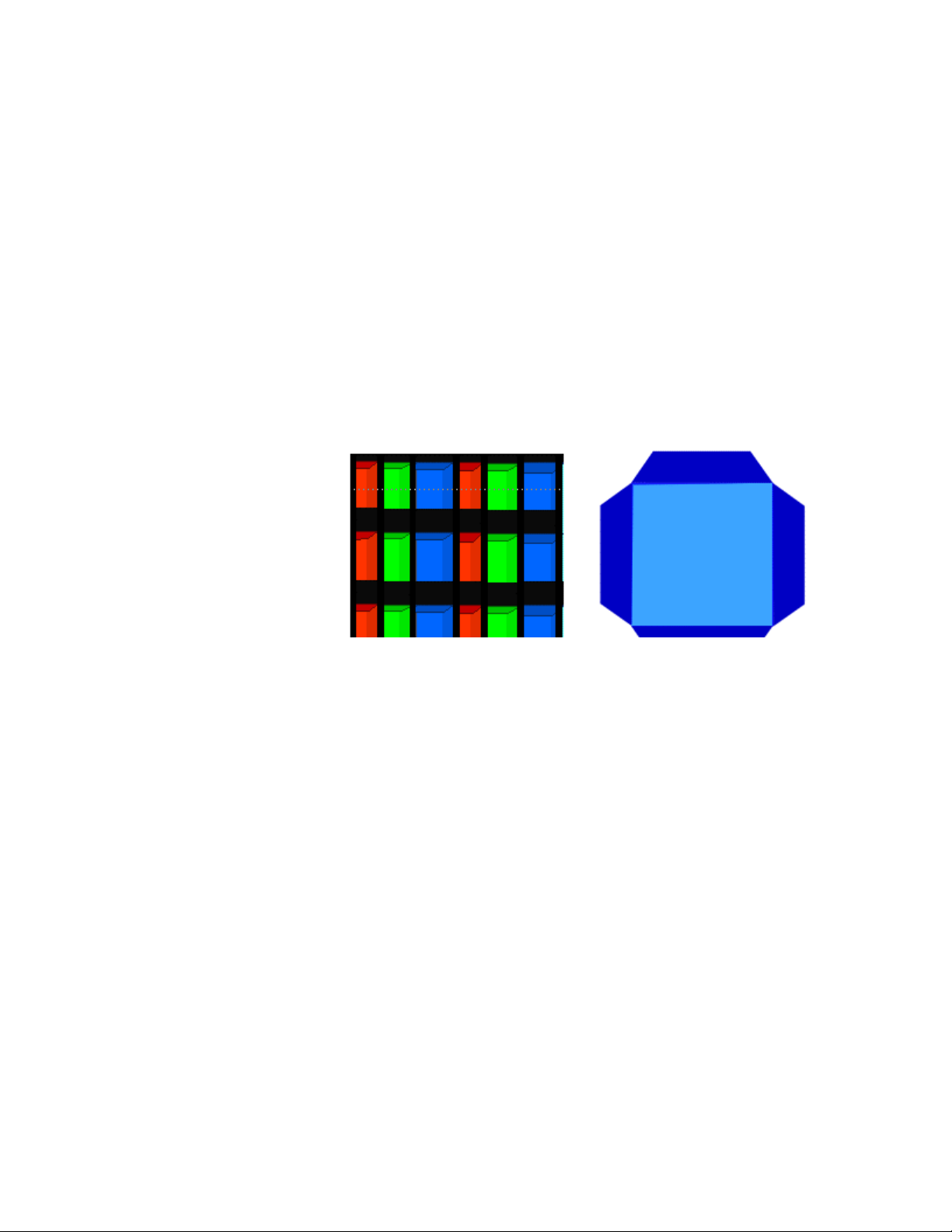
Number of Dots H 2556 x V 480
Pixel Size W 1.08 x H 1.08 mm
Drive Method AC Type Sub Field Drive System, Variable sub Field
Screen Size HD type 42” 16 x 9 (920 x 518 mm)
Number of
Pixels
Number of Dots H 3072 x V 768
Pixel Size W 0.90 x H 0.645 mm
Drive Method AC Type Sub Field Drive System, Variable sub Field
H 852 x 480 (VGA)
525i (480i), 525p (480p), 625i (575i), 625p (575p),
750p (720p), 1125 (1080)/60i, 50i, 24p, 24sf
VGA, SVGA, XGA, SXGA, UXGA
H 1024 x 768 (VGA)
Power Off 0.6W
525i (480i), 525p (480p), 625i (575i), 625p (575p),
750p (720p), 1125 (1080)/60i, 50i, 24p, 24sf, 1250
(1080)/50i
VGA, SVGA, XGA, SXGA, UXGA
9
New Features and Circuit Improvements
Integrated NTSC Tuner
3/2 Pulldown circuit
Plasma Contrast Auto Tracking System (C.A.T.S.)
Picture-in-Picture
SD models
• New Deep Black Front Glass Filter: Improves Contrast Ratio in Lighting
Environment
• Super Real Gamma System: Reproduces 1,536 shades of gradation
(60Hz)
• 10-bit Digital Processing: Reproduces
• DVI Input
HD models
• New 5 Facet
Asymmetrical
Cell Structure
Panel:
Improves
Brightness
Level
• New Real Black Drive System: Achieves greater than 4000:1 Contrast
Ratio in Dark Environments
• New Deep Black Front Glass Filter: Improves Contrast Ratio in Lighting
Environment by 80%
• Super Real Gamma System: Reproduces
• 10-bit Digital Processing: Reproduces 1,070 Million Colors
• SD / PC Card Reader- View images on screen from a digital camera
• HDMI Input with Analog Audio inputs
by 45%
by 15%
1,070-Million Colors
Figure 1
1,536 shades of gradation
10
SSiinnggllee SSccaann ((SSDD))
DDuuaall SSccaann ((HHDD))
Figure 2
•Simple and low cost circuit
•High performance
•Higher brightness
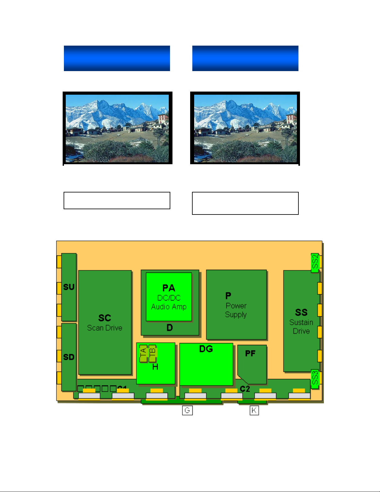
42” SD PCB Board Layout Diagram
Figure 2
11
Printed Circuit Board Information Table
Board Name Function
PF Fuse and Line Filter Circuit
P Power Supply Circuit
PA DC/DC converter and Audio Amplifier Circuit
K Remote, Light Receiver and Power LED Circuits
G Front Switch, PC and Video Input Circuits
D RGB Digital Processor, Format converter, Plasma AI,
Discharge Control Circuits, Sub-Field Processor
SC Scan Signal Drive Circuit
SU/SD Scan Signal Output Driver (Upper and Down side)
SS Sustain Signal Output Driver
SS2, SS3 Sustain Output Signal Extension Boards
C1 Data Pulse Connector for Right
C2 Data Pulse Connector for Left
TA Tuner (main)
TB Tuner (sub)
H A/V Switching and Video Input Circuits
DG Digital Core, MPU, RGB amp, and DVI Input Circuits
Board Comparison Chart
GP5 Chassis GP6 Chassis Board Function
C1 C1 Data Drive
C2 C2 Data Drive
D2 D RGB Digital Processor, Format converter,
Plasma AI, Discharge Control Circuits, Sub-Field
Processor
D1 DG Digital Core, MPU, RGB amp, and DVI Input
Circuits
V1 G Front Switch, PC and Video Input Circuits
HX and HZ
Boards
P P Power Supply Circuit
Z PA DC/DC and Audio Circuits
F PF Fuse and Line Filter Circuit
SC SC Scan Signal Drive Circuit
SD SD Scan Signal Output Driver (Lower Section)
SS SS Sustain Signal Output Driver
SS2 SS2 Sustain Output Signal Upper Boards
SS3 SS3 Sustain Output Signal Lower Boards
SU SU Scan Signal Output Driver (Upper Section)
N/A TA Tuner (Main)
N/A TB Tuner (Sub)
H A/V Switching and Video Input Circuits
12

Video Signal Block Diagram
Figure 3
GP6 series plasma panels incorporate two NTSC tuners. The main tuner is used
for primary picture operation. It provides a composite video and a multiplex audio
output. The sub-tuner provides only a video output used for multi picture
functions. The video outputs of the tuners are connected to the input switch IC on
the H Board. The unit also contains three video inputs that are also connected to
the input switch IC. The input switch IC selects one of the 5 video inputs for main
picture operation and another for sub-picture operation. Selection is controlled by
the MPU via the I
the main switch IC.
The panel also contains three component inputs and a DVI or HDMI input
(depending upon the model) that are connected to the main switch. The DVI or
HDMI input connector, connected to the DG Board, outputs the digital signal to
the DVI or HDMI receiver where it undergoes serial to parallel conversion. The
output of the receiver is then converted to a Y, Pb, and Pr component signals
before being applied to the Main switch. The MPU selects one of the 8 inputs for
main picture operation and another for sub-picture operation.
On the DG- Board, the global core IC (GC2M) converts the composite video
signal of the main picture to RGB video signals. The GC2S IC processes the
sub-picture information and combines it with the main picture. It performs
2
C Bus (SDA & SCL). These two outputs are then connected to
13

interlace to progressive scan conversion. The Global core IC also converts the
horizontal frequency of all NTSC inputs to 31.468KHz. The output of the GC2M
IC is RGB; it is applied to an external RGB amplifier.
IC001 is the TV Main CPU. It generates the On Screen Display (OSD) RGB
signals, which also enters the RGB amplifier stage. A switching circuit combines
the two sets of RGB signals for display on the screen. All NTSC, Component,
and RGB picture adjustments such as picture, tint, color, brightness, etc. are
performed inside this IC.
The RGB/PC select circuit switches between PC and all other inputs. The output
of the switch is routed to the D Board.
14
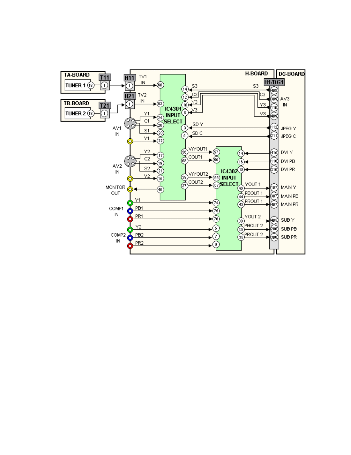
Video Signal Path Explanation
Figure 4
NTSC \ 480i Video Signal Path
The TH-42PA20U/P incorporates two NTSC tuners, allowing the simultaneous
viewing of two signals. It is also equipped with three NTSC Video inputs and
three NTSC S-Video inputs. Tuner-1 produces audio and video signals. Tuner-2
produces video only, as it is the video source intended for use in the “Picture in
Picture” mode. Video signals produced by the main tuner (tuner-1) and sub tuner
(tuner-2) are applied to the H-Board via pin 1 of the connector T11/H11 and pin 1
of the connector T21/H21. The signal applied to the AV3 video input, located at
the bottom of the front panel, enters the G-Board and passes through to the DGBoard without alteration. It is then applied to the H Board.
IC4301 on the H-Board selects the main video source and sub video source from
the NTSC inputs. The main Video or Luminance and chrominance signals are
output via pins 56 and 58. The sub video signal is output via pins 39 and 37. Both
15

Main and Sub Video signals are amplified and applied to another video switching
IC, IC4302.
The component video signals Y, Pb, and Pr are also input to IC4302 via the
connectors located at the rear of the cabinet.
The DVI input connector, attached to the DG Board, supplies the DVI signal to
the DVI receiver where it undergoes serial to parallel conversion. The output of
the DVI receiver is converted to a Y, Pb, and Pr component signal and then
applied to pins 14, 16, and 18 of IC4302 via pins 415, 116, and 316 of connector
H1/DG1. IC4302 selects between NTSC, Component, and DVI video input
signals. The selected signals can be in any of the three formats; Video, Y/C, or Y,
Pb, Pr. The main signal is output via pins 43, 44, and 46 of IC4302. The signals
are amplified and output to the DG-Board via pins 107, 307, and 407 of the
connector H1/DG1. The Sub NTSC video signals are also amplified and output to
the DG-Board via pins 405, 206, and 406 of the same connector.
16
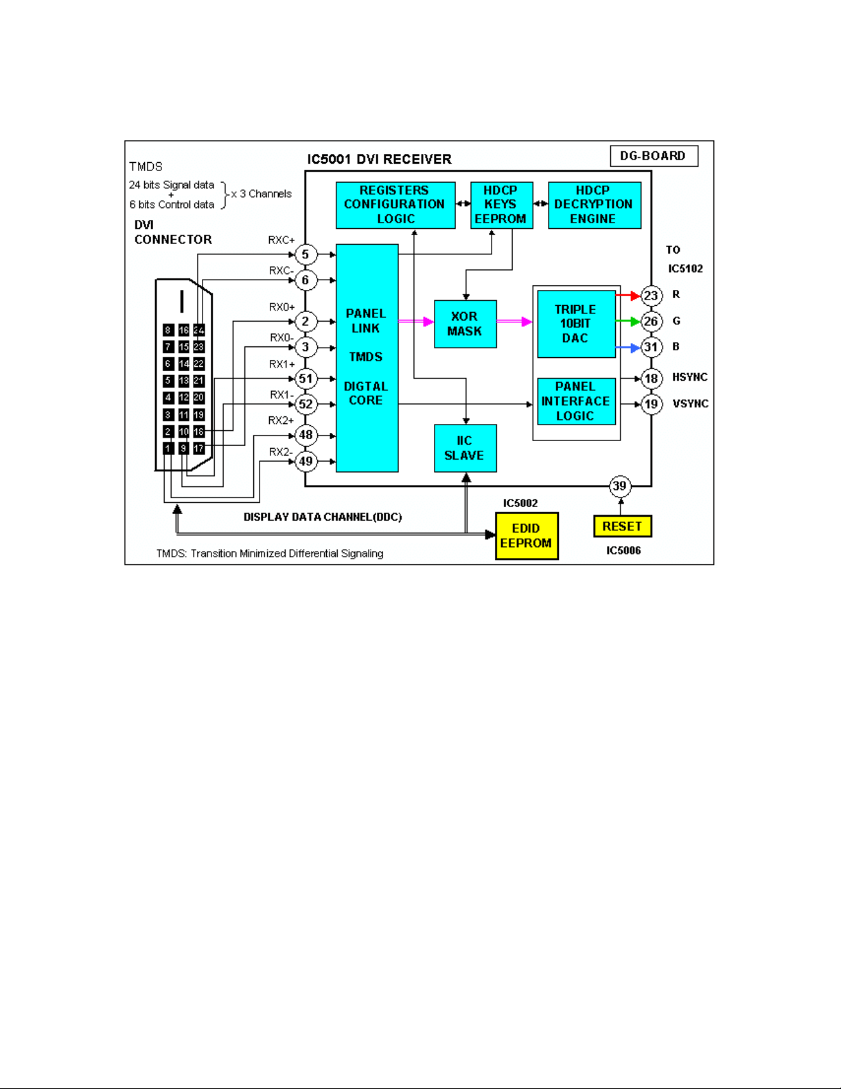
DVI Input
Figure 5
The DVI (Digital Visual Interface) input is a port designed to receive digital video
from a set-top box, a DVD player, or other digital devices. IC5001 converts the
digital video to parallel analog RGB video. The HDCP (High-bandwidth digital
content protection) circuit monitors the DVI signal for copyright protection. The
output of IC5001 is then applied to IC5102. The EDID EEPROM allows for
external control of the picture from the DVI source.
17
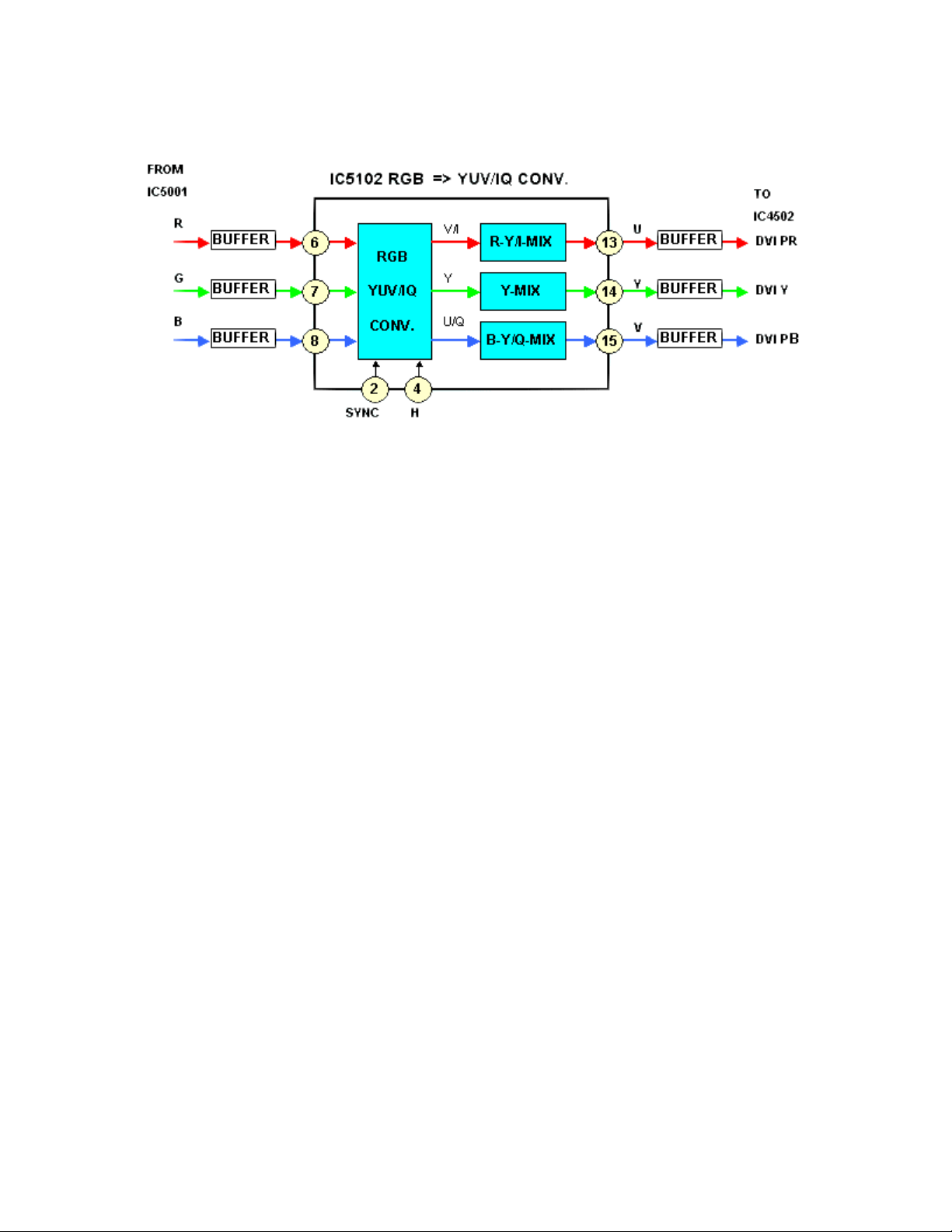
DVI RGB to YUV Conversion
Figure 6
IC5102 is an RGB to YUV (Y, Pb, PR) converter. It uses the vertical and
horizontal sync pulses of the DVI receiver to convert the analog RGB signal to Y,
Pb, Pr component signal. The signal is now in the form of an ATSC signal format
that can be processed like any other component signal. The output is sent to the
Main switch IC4302 for selection.
18
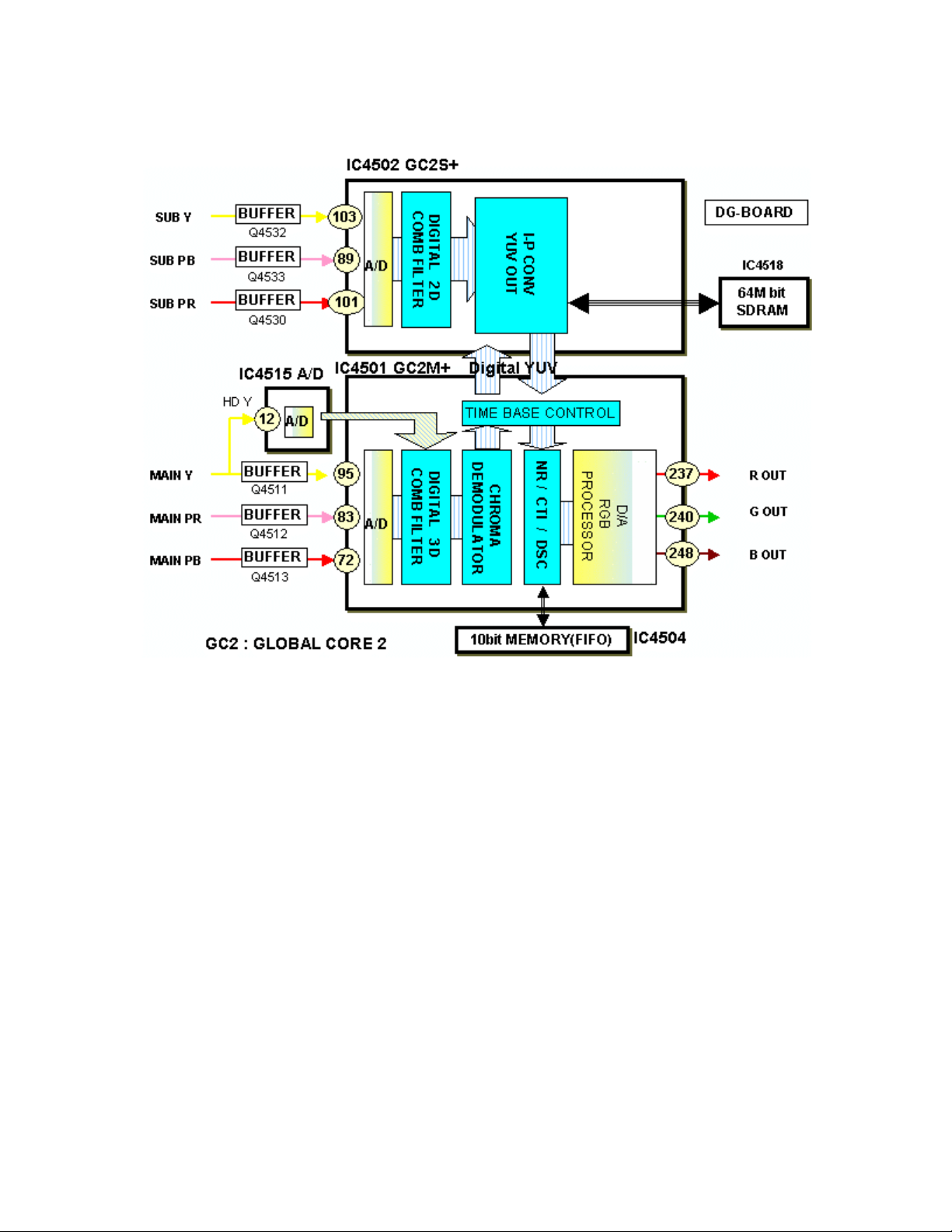
Digital Processor
Figure 7
Main Picture
On the DG- Board, the main Y, Pb, Pr signals are converted to digital data by an
analog to digital (A/D) converter circuit located inside the Global Core IC, IC4501.
The comb filter in IC4501 converts the composite video signal of the main picture
to Y and C separated video signals. S-Video, which is already Y/C separated,
simply passes through the comb filter. The data is then applied to the Chroma
demodulator circuit that separates the color signal into Pb and Pr data. If the
incoming video is in the 480p and 1080i format, the main Y signal is converted to
digital by IC4515 before being applied to IC4501. The A/D converter inside
IC4501 converts the color signals to digital. The data of the color signals bypass
the comb filter and Chroma demodulator circuits to join up with the luminance
data.
IC4501 outputs the data to the global core IC, IC4502. IC4502 contains a linedoubling circuit that halves the horizontal line period, doubling the horizontal
frequency to 31.468KHz. Using IC4518 as a temporary storage area, IC4502
19

then converts the digital signal scan format from interlaced to progressive before
sending it back to IC4501. The NR/CTI/DSC circuit reduces noise and improves
the picture quality. The 10 bit signals are then converted to analog R, G, and B
component signals by IC4501, and applied to the RGB amplifier IC4512.
Sub Picture
On the DG- Board, an analog to digital (A/D) converter circuit, located inside the
Sub Global Core IC4502, converts the sub Y, Pb, Pr signals to digital.
The data is then applied to a comb filter where luminance and chrominance are
separated.
IC4502 processes the Sub video data for use in the PIP mode. In this mode, the
main and sub video components are combined into one set of Y, Pb, and Pr
component signals.
The line-doubler, located inside the IC, halves the horizontal line period, doubling
the horizontal frequency to 31.468KHz. Using IC4518 as a temporary storage
area, IC4502 then converts the digital signal scan format from interlaced to
progressive before sending it back to IC4501. The NR/CTI/DSC circuit reduces
noise and improves the picture quality. The 10 bit digital signal is then converted
to analog R, G, and B component signals by IC4501, and applied to the RGB
amplifier IC4512.
20
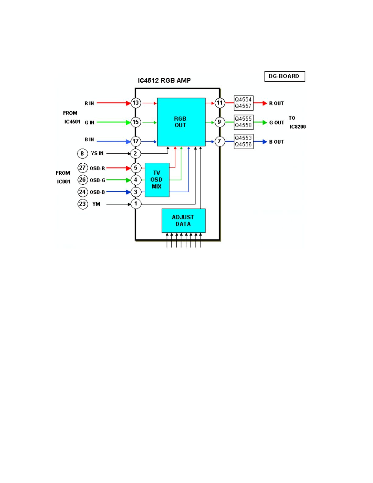
RGB Amplifier
Figure 8
The RGB output of IC4501 and the OSD (On Screen Display) RGB output of the
television MPU, IC001 enter the RGB amplifier IC4512. A switching circuit
combines the two RGB signals for display on the screen. The Adjust Data section
sets the RGB level, matching the required levels for the DG board. The output of
IC4512 enters IC8200 of the DG-Board for selection between PC and all other
inputs.
21
 Loading...