

Panasonic TH-37PV8, TH-37PX8B, TH-37PX8E, TH-42PV8P, TH-42PX8B Service manual
...
ORDER NO.PCZ0802011CE
Plasma Television
Model No. TH-37PV8P
TH-37PX8B
TH-37PX8E
TH-42PV8P
TH-42PX8B
TH-42PX8E
GPH11DE Chassis
© 2008 Matsushita Electric Industrial Co., Ltd. All
rights reserved. Unauthorized copying and distribution is a violation of law.
1 Safety Precautions
1.1. General Guidelines
1. When servicing, observe the original lead dress. If a short circuit is found, replace all parts which have been overheated or
damaged by the short circuit.
2. After servicing, see to it that all the protective devices such as insulation barriers, insulation papers shields are properly
installed.
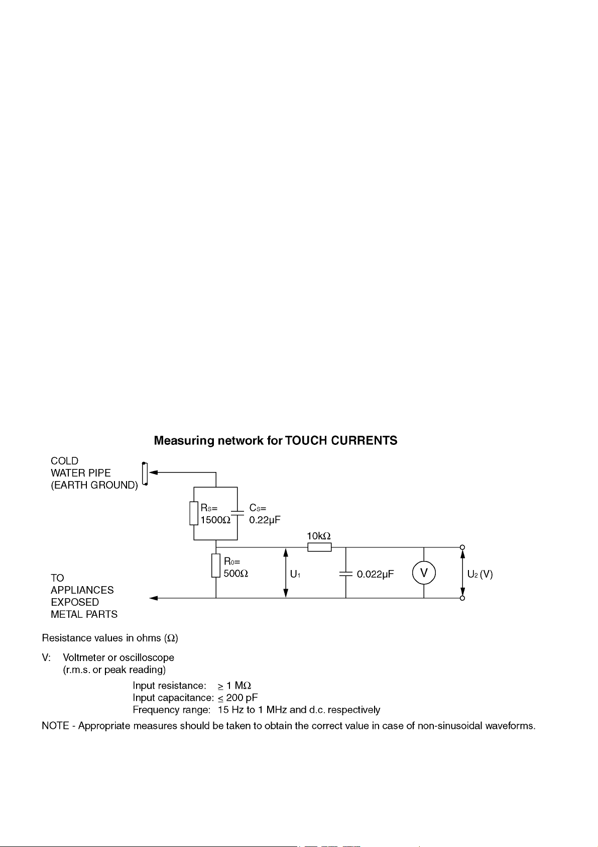
3. After servicing, make the following leakage current checks to prevent the customer from being exposed to shock hazards.
4. When servicing, observe the original lead dress. If a short circuit is found, replace all parts which have been overheated or
damaged by the short circuit.
5. After servicing, see to it that all the protective devices such as insulation barriers, insulation papers shields are properly
installed.
6. After servicing, make the following leakage current checks to prevent the customer from being exposed to shock hazards.
1.2. Touch-Current Check
1. Plug the AC cord directly into the AC outlet. Do not use an isolation transformer for this check.
2. Connect a measuring network for touch currents between each exposed metallic part on the set and a good earth ground
such as a water pipe, as shown in Figure 1.
3. Use Leakage Current Tester (Simpson 228 or equivalent) to measure the potential across the measuring network.
4. Check each exposed metallic part, and measure the voltage at each point.
5. Reserve the AC plug in the AC outlet and repeat each of the above measure.
6. The potential at any point (TOUGH CURRENT) expressed as voltage U
For a. c.: U1 = 35 V (peak) and U2 = 0.35 V (peak);
For d. c.: U1 = 1.0 V,
Note:
The limit value of U
mA d. c.
The limit value U
7. In case a measurement is out of the limits specified, there is a possibility of a shock hazard, and the equipment should be
repaired and rechecked before it is returned to the customer.
= 0.35 V (peak) for a. c. and U1 = 1.0 V for d. c. correspond to the values 0.7 mA (peak) a. c. and 2.0
2
= 35 V (peak) for a. c. correspond to the value 70 mA (peak) a. c. for frequencies greater than 100 kHz.
1
and U2, does not exceed the following values:
1
Figure 1
2
2 Warning
2.1. Prevention of Electrostatic Discharge (ESD) to Electrostatically Sensitive (ES) Devices
Some semiconductor (solid state) devices can be damaged easily by static electricity. Such components commonly are called Electrostatically Sensitive (ES) Devices. Examples of typical ES devices are integrated circuits and some field-effect transistors and
semiconductor [chip] components. The following techniques should be used to help reduce the incidence of component damage
caused by electrostatic discharge (ESD).
1. Immediately before handling any semiconductor component or semiconductor-equipped assembly, drain off any ESD on your
body by touching a known earth ground. Alternatively, obtain and wear a commercially available discharging ESD wrist strap,
which should be removed for potential shock reasons prior to applying power to the unit under test.
2. After removing an electrical assembly equipped with ES devices, place the assembly on a conductive surface such as aluminum foil, to prevent electrostatic charge buildup or exposure of the assembly.
3. Use only a grounded-tip soldering iron to solder or unsolder ES devices.
4. Use only an anti-static solder removal device. Some solder removal devices not classified as [anti-static (ESD protected)] can
generate electrical charge sufficient to damage ES devices.
5. Do not use freon-propelled chemicals. These can generate electrical charges sufficient to damage ES devices.
6. Do not remove a replacement ES device from its protective package until immediately before you are ready to install it. (Most
replacement ES devices are packaged with leads electrically shorted together by conductive foam, aluminum foil or comparable conductive material).
7. Immediately before removing the protective material from the leads of a replacement ES device, touch the protective material
to the chassis or circuit assembly into which the device will be installed.
Caution
Be sure no power is applied to the chassis or circuit, and observe all other safety precautions.
8. Minimize bodily motions when handling unpackaged replacement ES devices. (Otherwise ham less motion such as the brushing together of your clothes fabric or the lifting of your foot from a carpeted floor can generate static electricity (ESD) sufficient
to damage an ES device).
3
2.2. About lead free solder (PbF)
Note: Lead is listed as (Pb) in the periodic table of elements.
In the information below, Pb will refer to Lead solder, and PbF will refer to Lead Free Solder.
The Lead Free Solder used in our manufacturing process and discussed below is (Sn+Ag+Cu).
That is Tin (Sn), Silver (Ag) and Copper (Cu) although other types are available.
This model uses Pb Free solder in it’s manufacture due to environmental conservation issues. For service and repair work, we’d
suggest the use of Pb free solder as well, although Pb solder may be used.
PCBs manufactured using lead free solder will have the PbF within a leaf Symbol PbF stamped on the back of PCB.
Caution
• Pb free solder has a higher melting point than standard solder. Typically the melting point is 50 ~ 70 °F (30~40 °C) higher. Please
use a high temperature soldering iron and set it to 700 ± 20 °F (370 ± 10 °C).
• Pb free solder will tend to splash when heated too high (about 1100 °F or 600 °C).
If you must use Pb solder, please completely remove all of the Pb free solder on the pins or solder area before applying Pb solder. If this is not practical, be sure to heat the Pb free solder until it melts, before applying Pb solder.
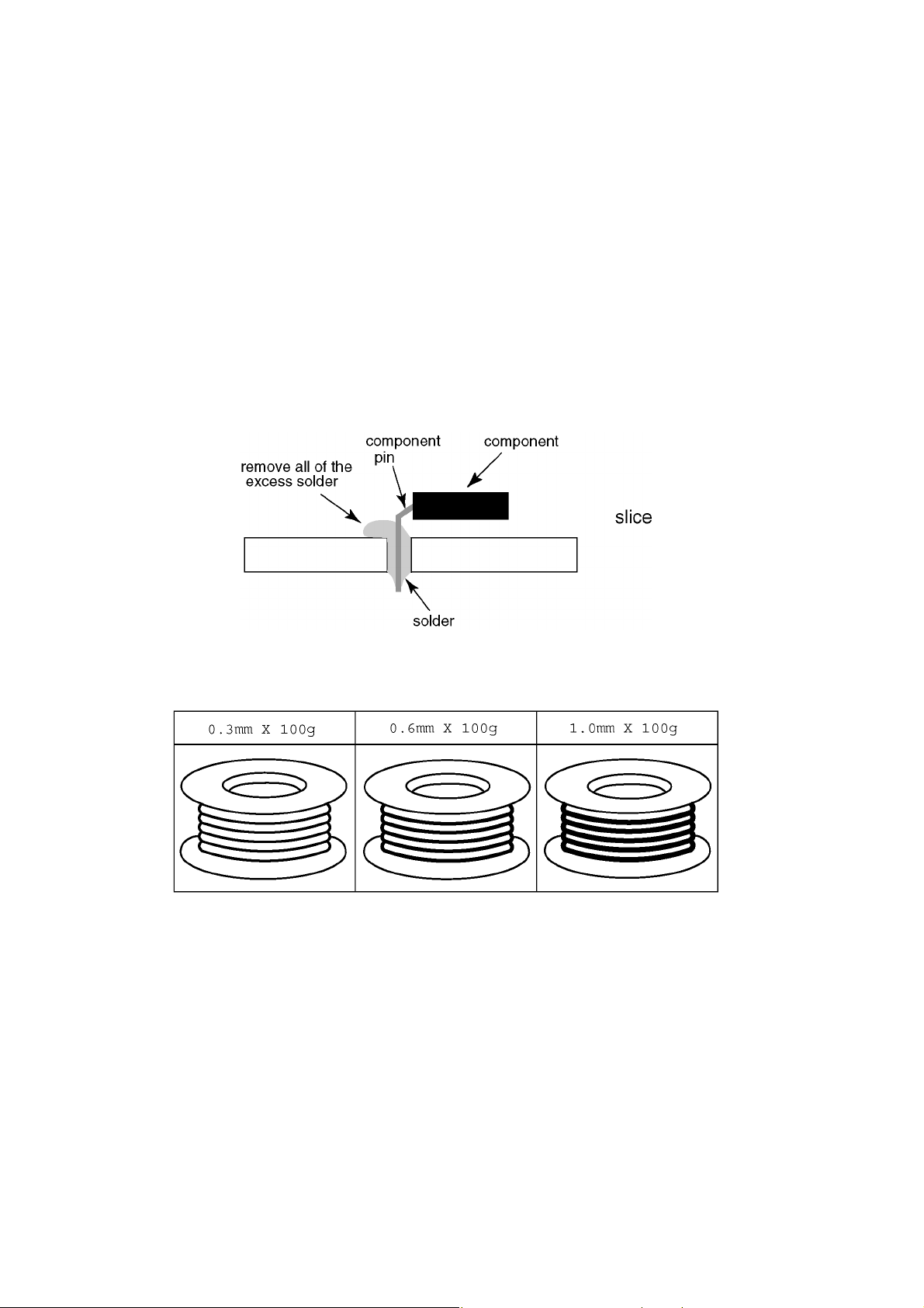
• After applying PbF solder to double layered boards, please check the component side for excess solder which may flow onto the
opposite side. (see figure below)
Suggested Pb free solder
There are several kinds of Pb free solder available for purchase. This product uses Sn+Ag+Cu (tin, silver, copper) solder. However, Sn+Cu (tin, copper), Sn+Zn+Bi (tin, zinc, bismuth) solder can also be used.
4
3 Service Navigation
3.1. Service Hint (42 inch)
Board Name Function Board Name Function
P Power Supply C1 Data Driver (Lower Right)
A DC-DC Converter
Speaker out, Sound Processor
AV Terminal, AV Switch
Digital Signal Processor, Micon, HDMI Interface
Peaks Lite 2p
Format Converter, Plasma AI, Sub-Field Processor
K Remote receiver, Power LED GS SD Card Slot
S Power Switch
C2 Data Driver (Lower Left)
SC Scan Drive
SU Scan out (Upper)
SD Scan out (Lower)
SS Sustain Drive
G Key Switch, Front Terminal
5
3.2. Service Hint (37 inch)
Board Name Function Board Name Function
P Power Supply C1 Data Driver (Lower Right)
A DC-DC Converter
Speaker out, Sound Processor
AV Ter minal , AV S w itch
Digital Signal Processor, Micon, HDMI Interface
Peaks Lite 2p
Format Converter, Plasma AI, Sub-Field Processor
K Remote receiver, Power LED S Power Switch
C2 Data Driver (Lower Left)
SC Scan Drive
SM Scan out
SS Sustain Drive
G Key Switch, Front Terminal
GS SD Card Slot
6
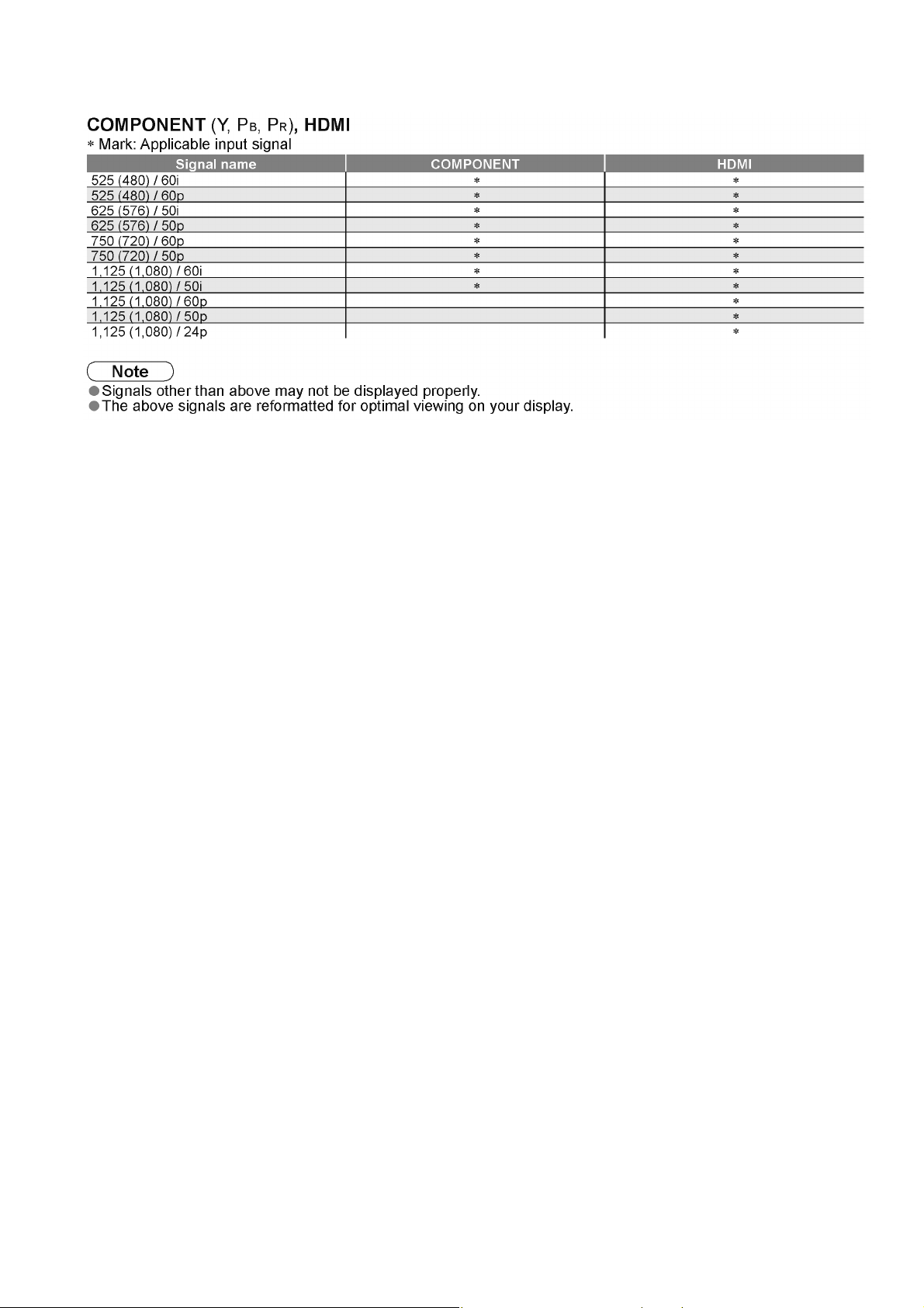
3.3. Applicable signals
7

4 Specifications
Power Source AC 220 - 240 V, 50/60 Hz
Power Consumption
Average use 235 W (37 inch)
Standby condition 0.7 W (Without monitor out recording)
Plasma Display panel
Aspect Ratio 16:9
Visible screen size 94 cm (diagonal) (37 inch)
Number of pixels 737,280 (1,024 (W) × 720 (H)) [3,072 × 720 dots] (37 inch)
Sound
Speaker 160 mm × 42 mm × 2 pcs, 8 Ω
Audio Output 20 W (10 W + 10 W), 10% THD
Headphones M3 (3.5 mm) stereo mini Jack × 1
Receiving Systems / Band name PAL I : UHF E21-68
(B model) PAL 525/60 : Playback of NTSC tape from some PAL Video recorders (VCR)
(Except B model) PAL B, G, H, I, SECAM B, G, SECAM L/L’ :
Aerial - Rear UHF (B model), VHF/UHF (Except B model)
Operating Conditions
Connection Terminals
AV1 (Scart terminal) 21 Pin terminal (Audio/Video in, Audio/Video out, RGB in, Q-Link)
AV2 (Scart terminal) 21 Pin terminal (Audio/Video in, Audio/Video out, RGB in, S-Video in, Q-Link)
AV3
VIDEO RCA PIN Type × 1 1.0 V [p-p] (75 Ω)
S-VIDEO Mini DIN 4-pin Y:1.0 V [p-p] (75 Ω) C:0.286 V [p-p] (75 Ω)
AUDIO L - R RCA PIN Type × 2 0.5 V [rms]
COMPONENT
VIDEO
AUDIO L - R RCA PIN Type × 2 0.5 V [rms]
Others
HDMI1 / 2 TYPE A Connectors This TV supports “HDAVI Control 3” function.
Output
AUDIO L - R RCA PIN Type × 2 0.5 V [rms] (high impedance)
Dimensions (W × H × D) 917 mm × 665 mm × 327 mm (With Pedestal) (37 inch)
Mass 24.0 kg Net (With Pedestal) (37 inch)
255 W (42 inch)
20 W (With monitor out recording)
819 mm (W) × 457 mm (H) (37 inch)
106 cm (diagonal) (42 inch)
922 mm (W) × 518 mm (H) (42 inch)
786,432 (1,024 (W) × 768 (H)) [3,072 × 768 dots] (42 inch)
or NTSC disc playback from DVD player and recorder.
DVB : Digital terrestrial services via UHF aerial input.
M.NTSC : Playback from M.NTSC Video recorders (VCR).
NTSC (AV input only) : Playback from NTSC Video recorders (VCR).
VHF E2 - E12 VHF H1 - H2 (ITALY)
VHF A - H (ITALY) UHF E21 - E69
CATV (S01 - S05) CATV S1 - S10 (M1 - M10)
CATV S11 - S20 (U1 - U10) CATV S21 - S41 (Hyperband)
PAL D, K, SECAM D, K :
VHF R1 - R2 VHF R3 - R5
VHF R6 - R12 UHF E21 -E69
PAL 520/60 : Playback of NTSC tape from some PAL Video recorders (VCR)
DVB : Digital terrestrial services via VHF / UHF aerial input.
M.NTSC : Playback from M. NTSC Video recorders (VCR)
NTSC (AV input only) : Playback from NTSC Video recorders (VCR)
Temperature: 0 °C - 35 °C
Humidity: 20 % - 80 % RH (non-condensing)
Y 1.0 V [p-p] (including synchronization)
P
, P
B
R
917 mm × 617 mm × 92.5 mm (TV only) (37 inch)
1,020 mm × 727 mm × 327 mm (With Pedestal) (42 inch)
1,020 mm × 679 mm × 92.5 mm (TV only) (42 inch)
22.0 kg Net (TV only) (37 inch)
27.5 kg Net (With Pedestal) (42 inch)
25.5 kg Net (TV only) (42 inch)
± 0.35 V [p-p]
Note
• Design and Specifications are subject to change without notice. Mass and Dimensions shown are approximate.
8

• This equipment complies with the EMC standards listed below.
EN55013, EN61000-3-2, EN61000-3-3, EN55020.
9
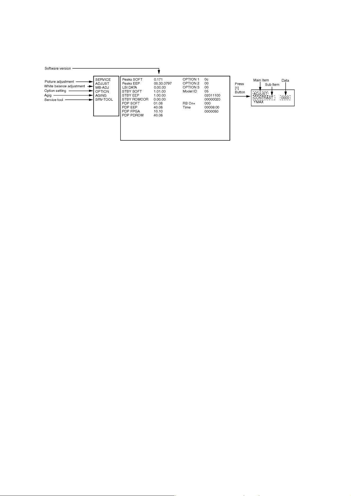
5 Service Mode
5.1. How to enter into Service Mode
While pressing [VOLUME ( - )] button of the main unit, press [0] button of the remote control three times within 2 seconds.
5.1.1. Key command
[1] button...Main items Selection in forward direction
[2] button...Main items Selection in reverse direction
[3] button...Sub items Selection in forward direction
[4] button...Sub items Selection in reverse direction
[RED] button...All Sub items Selection in forward direction
[GREEN] button...All Sub items Selection in reverse direction
[VOL] button...Value of sub items change in forward direction ( + ), in reverse direction ( - )
10
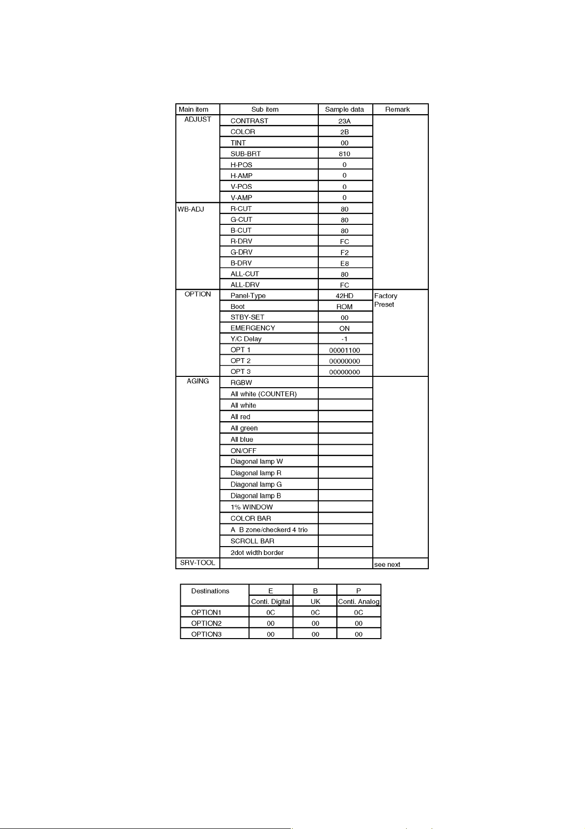
5.1.2. Contents of adjustment mode
• Value is shown as a hexadecimal number.
• Preset value differs depending on models.
• After entering the adjustment mode, take note of the value in each item before starting adjustment.
5.1.3. How to exit
Switch off the power with the [POWER] button on the main unit or the [POWER] button on the remote control.
11
5.2. Service tool mode
5.2.1. How to access
1. Select [SRV-TOOL] in Service Mode.
2. Press [OK] button on the remote control.
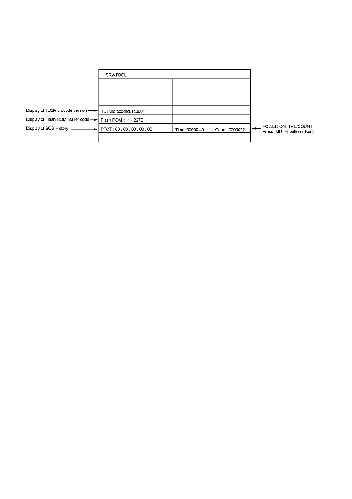
5.2.2. Display of SOS History
SOS History (Number of LED blinking) indication.
From left side; Last SOS, before Last, three occurrence before, 2nd occurrence after shipment, 1st occurrence after shipment.
This indication will be cleared by [Self-check indication and forced to factory shipment setting].
5.2.3. POWER ON TIME/COUNT
To display TIME/COUNT menu, highlight position, then press MUTE for 3sec.
Time : Cumulative power on time, indicated hour : minute by decimal
Count : Number of On times by decimal
Note : This indication will not be cleared by either of the self-checks or any other command.
5.2.4. Exit
1. Disconnect the AC cord from wall outlet or switch off the power with the [POWER] button on the main unit.
12
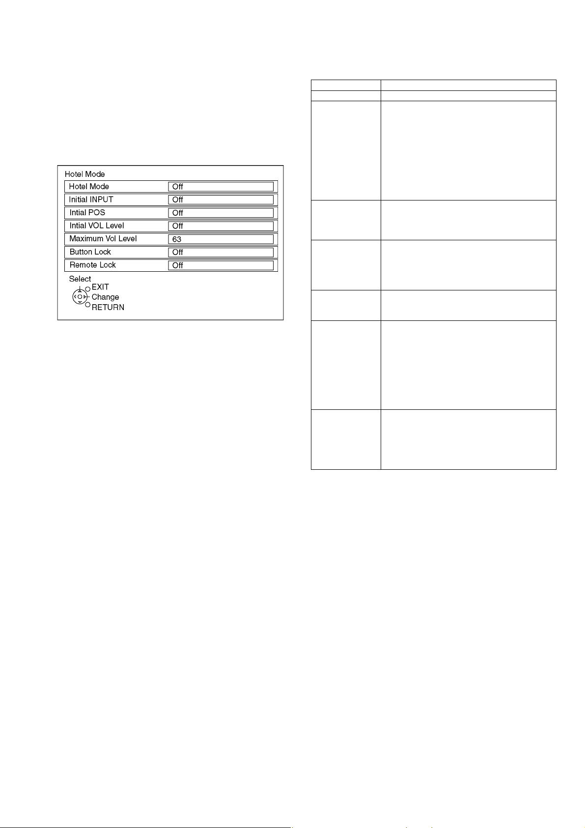
5.3. Hotel mode
1. Purpose
Restrict a function for hotels.
2. Access command to the Hotel mode setup menu
In order to display the Hotel mode setup menu, please
enter the following command (within 2 second).
[TV] : Vol. [Down] + [REMOTE] : AV (3 times)
Then, the Hotel mode setup menu is displayed.
3. To exit the Hotel mode setup menu
Disconnect AC power cord from wall outlet or switch off
the power with the [POWER] button on the main unit.
4. Explain the Hotel mode setup menu
item Function
Hotel Mode Select hotel mode ON/OFF
Initial INPUT Select input signal modes.
Set the input, when each time power is switched
on.
Selection :
Off/Analog/DVB/AV1/AV2/AV2S/COMPONENT/
HDMI1/HDMI2
• Off: give priority to a last memory. However,
Euro model is compulsorily set to TV.
• AVnS/AVnC: only Euro model selectable
• PC: selectable with VGA option
Initial POS Select programme number.
Selection :
Off/0 to 99
• Off: give priority to a last memory
Initial VOL level Adjust the volume when each time power is
switched on.
Selection/Range :
Off/0 to 63
• Off: give priority to a last memory
Maximum VOL
level
Button lock Select local key conditions.
Remote lock Select remote control key conditions.
Adjust maximum volume.
Range :
0 to 63
Selection :
Off/SETUP/MENU/All
• Off: altogether valid
• SETUP: only F-key is invalid
(Tuning guide(menu) can not be selected.)
• MENU: only F-key is invalid
(only Volume/Mute can be selected.)
• ALL: altogether invalid.
Selection :
Off/SETUP/MENU
• Off: altogether valid
• SETUP: only Setup menu is invalid
• MENU: Picture/Sound/Setup menu are invalid
13
6 Troubleshooting Guide
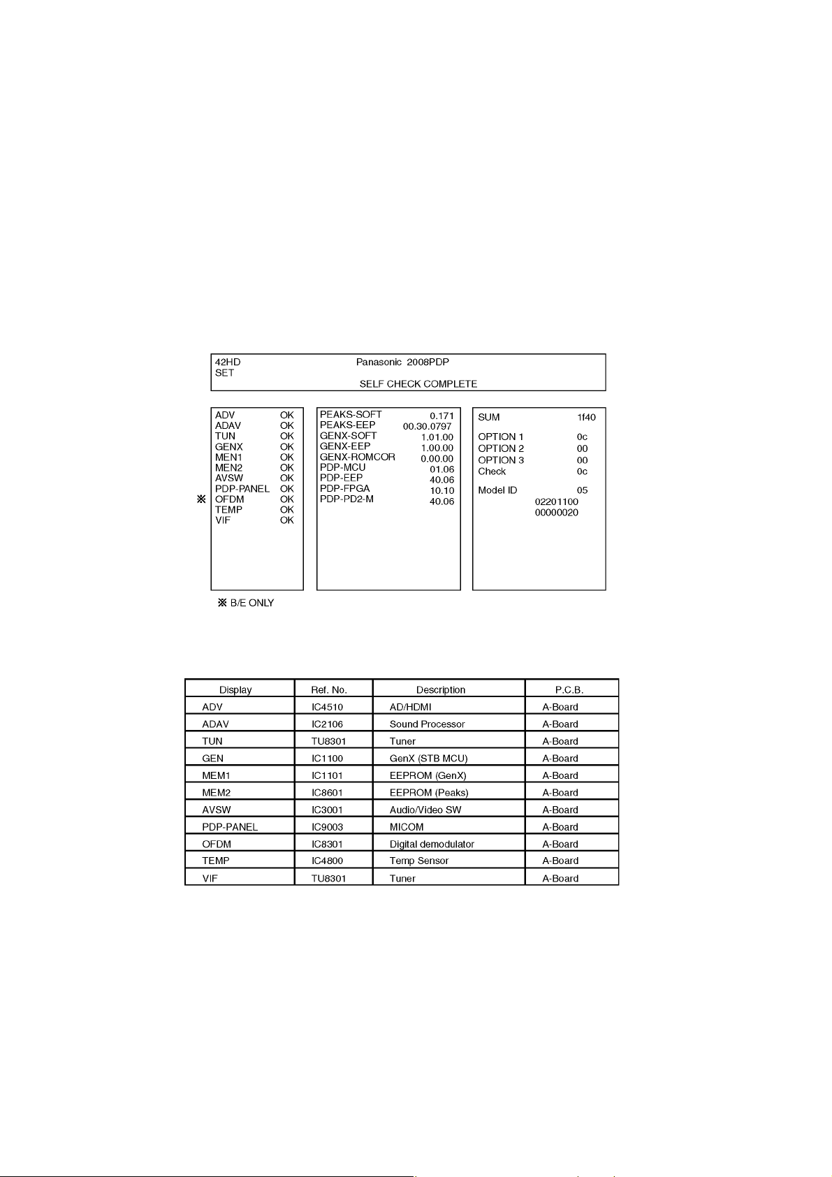
Use the self-check function to test the unit.
1. Checking the IIC bus lines
2. Power LED Blinking timing
6.1. Check of the IIC bus lines
6.1.1. How to access
Self-check indication only:
Produce TV reception screen, and while pressing [VOLUME ( - )] button on the main unit, press [OK] button on the remote control
for more than 3 seconds.
Self-check indication and forced to factory shipment setting:
Produce TV reception screen, and while pressing [VOLUME ( - )] button on the main unit, press [MENU] button on the remote con-
trol for more than 3 seconds.
6.1.2. Screen display
6.1.3. Check Point
Confirm the following parts if NG was displayed.
6.1.4. Exit
Disconnect the AC cord from wall outlet or switch off the power with the [POWER] button on the main unit.
14
6.2. Power LED Blinking timing chart
1. Subject
Information of LED Flashing timing chart.
2. Contents
When an abnormality has occurred the unit, the protection circuit operates and reset to the stand by mode. At this time, the
defective block can be identified by the number of blinks of the Power LED on the front panel of the unit.
15
6.3. No Power
First check point
There are following 2 states of No Power indication by power LED.
1. No lit
2. Red is lit then turns red blinking a few seconds later. (See 6.2.)
16
6.4. No Picture
17
6.5. Local screen failure
Plasma display may have local area failure on the screen. Fig-1 is the possible defect P.C.B. for each local area.
Fig-1
18
7 Disassembly and Assembly Instructions
7.1. Remove the rear cover
1. See Service Hint (Section 5)
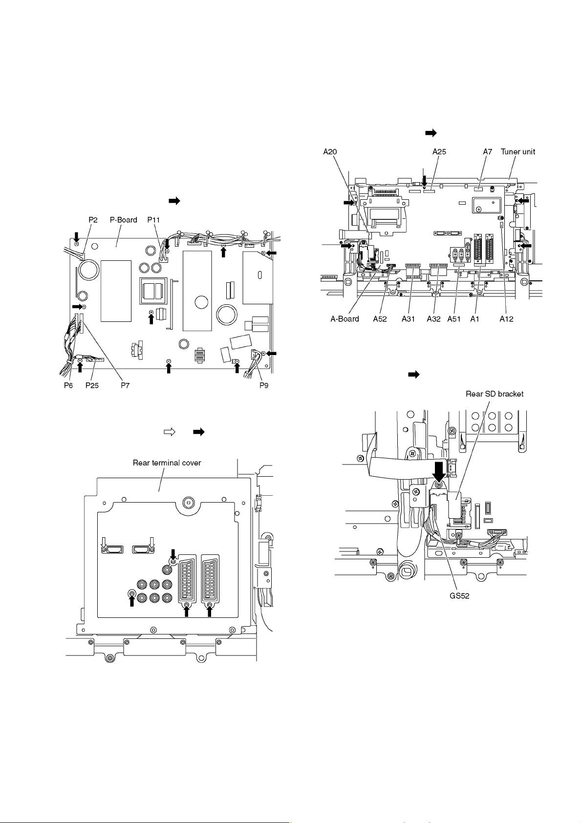
7.2. Remove the P-Board
Caution:
To remove P.C.B. wait 1 minute after power was off for discharge from electrolysis capacitors.
1. Unlock the cable clampers to free the cable.
2. Disconnect the connectors (P2, P6, P7, P9, P11, P12 and
P25).
3. Remove the screws (×10 ) and remove the P-Board.
7.4. Remove the Tuner unit
1. Unlock the cable clampers to free the cable.
2. Disconnect the connectors (A1, A7, A12, A25, A31, A32,
A51, A52).
3. Remove the screws (×5 ) and remove the tuner unit.
7.5. Remove the GS-Board
1. Disconnect the connector (GS52).
2. Remove the screw ( ) and remove the rear SD bracket.
7.3. Remove the rear terminal cover
1. Remove the screws (×2 , ×4 ).
2. Remove the rear terminal cover.
19
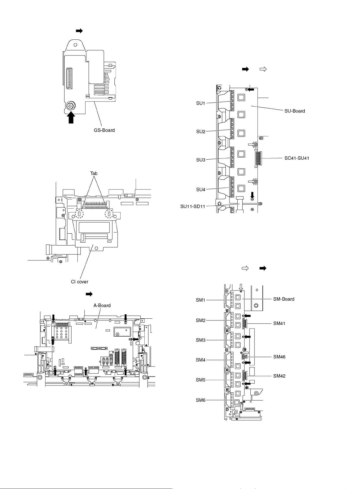
3. Remove the screw ( ) and remove the GS-Board.
7.6. Remove the A-Board
1. Remove the tuner unit. (See section 7.4.)
2. Remove the tab and remove the CI cover.
7.7. Remove the SU-Board (42 inch)
1. Remove the flexible cables (SU1, SU2, SU3 and SU4)
connected to the SU-Board.
2. Remove the flexible cable (SU11-SD11) and the bridge
connector (SC41-SU41).
3. Remove the screws (×2 , ×2 ) and remove the SU-
Board.
3. Remove the screws (×7 ) and remove the A-Board.
7.8. Remove the SM-Board
(37 inch)
1. Remove the flexible cables (SM1, SM2, SM3, SM4, SM5
and SM6).
2. Remove the bridge connector (SM41, SM42 and SM46).
3. Remove the screws (×3 , ×4 ) and remove the SM-
Board.
20
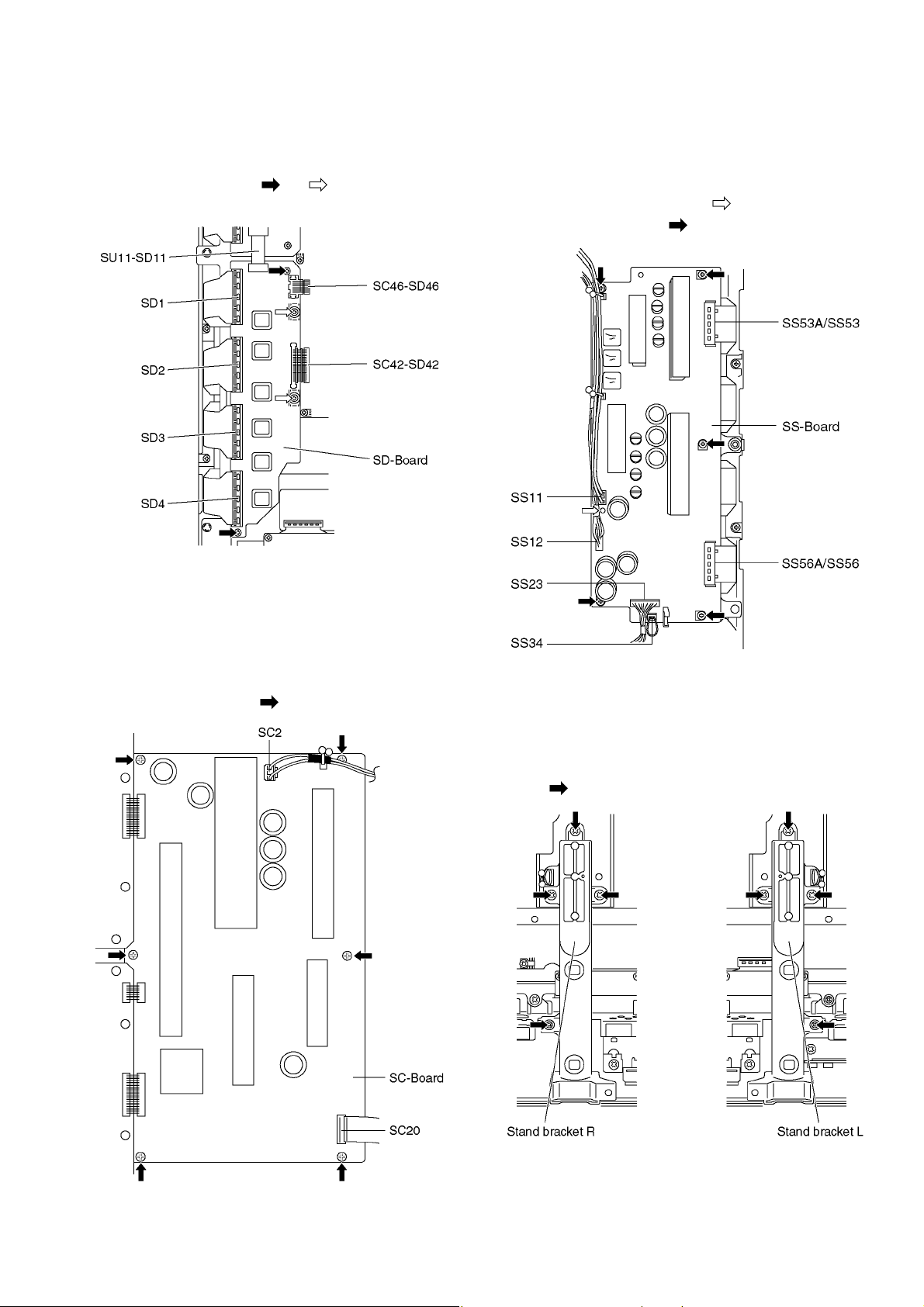
7.9. Remove the SD-Board (42 inch)
1. Remove the flexible cables (SD1, SD2, SD3 and SD4)
connected to the SD-Board.
2. Remove the flexible cable (SU11-SD11) and the bridge
connectors (SC42-SD42 and SC46-SD46).
3. Remove the screws (×2 , ×2 ) and remove the SD-
Board.
7.11. Remove the SS-Board
1. Unlock the cable clampers to free the cable.
2. Disconnect the connectors (SS11, SS12, SS23 and
SS34).
3. Disconnect the flexible cables (SS53A and SS56A) (42
inch)/(SS53 and SS56) (37 inch).
4. Remove the molding prop (×1 ).
5. Remove the srews (×5 ) and remove the SS-Board.
7.10. Remove the SC-Board
1. Remove the SU-Board, SM-Board and SD-Board. (See
section 7.7., 7.8. and 7.9.)
2. Unlock the cable clampers to free the cable.
3. Disconnect the connector (SC2).
4. Disconnect the flexible cable (SC20).
5. Remove the screws (×6 ) and remove the SC-Board.
7.12. Remove the stand brackets
1. Remove the plasma panel section from the servicing
stand and lay on a fiat surface such as a table (covered)
with the plasma panel surface facing downward.
2. Remove the stand brackets (left, right) fastening screws
(×4 each) and remove the stand brackets (left, right).
21
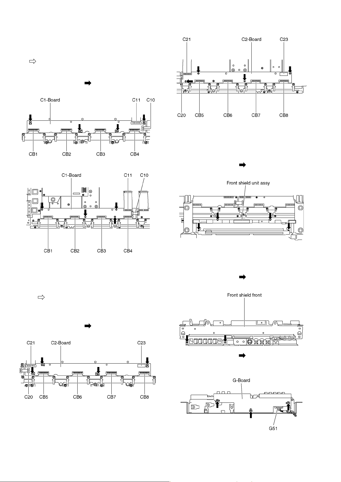
7.13. Remove the C1-Board
1. Remove the tuner unit. (See section 7.4.)
2. Unlock the cable clampers to free the cable.
3. Remove the flexible cables holder fastening screws (×8
).
4. Disconnect the flexible cables (CB1, CB2, CB3 and CB4).
5. Disconnect the flexible cables (C10 and C11).
6. Remove the screws (×4 ) and remove the C1-Board.
42 inch
37 inch
37 inch
7.15. Remove the front shield unit
assy
1. Disconnect the connector (A51 and A52). (See section
7.4.)
2. Remove the screws (×4 ) and remove the front shield
unit assy.
7.14. Remove the C2-Board
1. Remove the tuner unit. (See section 7.4.)
2. Unlock the cable clampers to free the cable.
3. Remove the flexible cables holder fastening screws
(×8 ).
4. Disconnect the flexible cables (CB5, CB6, CB7 and CB8).
5. Disconnect the flexible cables (C20 and C21).
6. Disconnect the connector (C23).
7. Remove the screws (×4 ) and remove the C2-Board.
42 inch
7.16. Remove the G-Board
1. Remove the front bracket and the front shield unit assy.
(See section 7.15.)
2. Remove the screws (×2 ) and remove the front shield
front.
3. Remove the screws (×5 ) and disconnect the connector (G51).
4. Remove the G-Board.
22
7.17. Remove the speaker L, R
1. Disconnect the connector (A12). (See section 7.4.)
2. Remove the screws (×4 each) and remove the
speaker L, R.
7.18. Remove the S-Board
1. Remove the stand brackets. (See section 7.12.)
2. Remove the screws (×2 ).
3. Disconnect the connector (S1).
7.19. Remove the K-Board
1. Remove the S-Board. (See section 7.18.)
2. Unlock the cable clampers to free the cable.
3. Remove the screws (×2 ).
4. Disconnect the connectors (K1) and remove the K-Board.
7.20. Remove the Plasma panel section from the Cabinet assy
(glass)
1. Remove the stand brackets (left, right) fastening screw
(×1 each).
4. Remove the screws (×2 ) and remove the S-Board.
2. Remove the cabinet assy and the plasma panel fastening
23
screws (×7 ).
3. For leaving the plasma panel from the front frame, pull the
bottom of the cabinet assy forward, lift, and remove.
5. Remove the BC hook (left, right).
4. Remove the spacers and spacer rings (×6).
Caution:
• Please confirm the installation of BC hook (Left, right),
Spacer and Spacer Ring when you exchange the Plasma
Panel, and install BC hook (Left, right), Spacer and Spacer
Ring in an original installation place after exchanging the
Plasma Panel.
7.21. Replace the plasma panel (finished)
1. Place the new plasma panel (finished) on the flat surface
of the table (covered by a soft cloth), with the plasma
panel surface facing downward.
2. Attach the C1-Board and the C2-Board, connect the flexible cables (×16) from the Plasma panel to the C1-Board
and the C2-Board, and fit the flexible cable holders.
3. Attach the Hooks (left, right) and fit the stand brackets (L,
R) to the new plasma panel.
4. Place the plasma panel section on the servicing stand.
5. Attach the cabinet assy and each P.C.Board and so on, to
the new plasma panel.
*When fitting the cabinet assy, be careful not to allow
any debris, dust or handling residue to remain
between the front glass and plasma panel.
24
8 Measurements and Adjustments
8.1. Driver Set-up
8.1.1. Item / Preparation
1. Input a white signal to plasma video input.
2. Set the picture controls as follows.
Picture menu: Dynamic
PNR: OFF
Aspect: 16:9
Caution
1. First perform Vsus adjustment.
2. Confirmation of Vscn voltage should be performed after
confirmation of Vad adjustment.
When Vad=-149V, Voltage of Vscn is -4V ±4V.
8.1.2. Adjustments
Adjust driver section voltages referring the panel data on the
panel data label.
Check or adjust the following voltages with the multimeter.
Name Test Point Voltage Volume Remarks
Vsus TPVSUS
(SS)
Ve TPVE (SS) Ve ± 1V VR16000 (SS) *
Vset TPVSET
(SC)
Vad TPVAD (SC) -149V ± 1V VR16600 (SC)
Vscn TPVSCN
(SC)
Vda TPVDA (SS) 75V ± 1V, -2V Fixed
*See the Panel label.
Vsus ± 2V R628 (P) *
320V ± 7V Fixed
Vad+145V ± 4V Fixed
25
8.1.3. P.C.B. (Printed Circuit Board) exchange
8.1.3.1. Caution
1. To remove P.C.B. , wait 1 minute after power was off for discharge from electrolysis capacitors.
8.1.3.2. Quick adjustment after P.C.B. exchange
Adjust the following voltages with the multimeter.
P.C.B. Name Test Point Voltage Volume Remarks
P Board Vsus TPVSUS (SS) Vsus ± 2V R628 (P) *
SC Board Vad TPVAD (SC) -105V ± 1V VR16600 (SC)
SS Board Ve TPVE (SS) Ve ± 1V VR16000 (SS) *
*See the Panel label.
Caution:
Absolutely do not reduce Vsus below Ve not to damage the P.C.B.
8.1.4. Adjustment Volume Location
8.1.5. Test Point Location
26
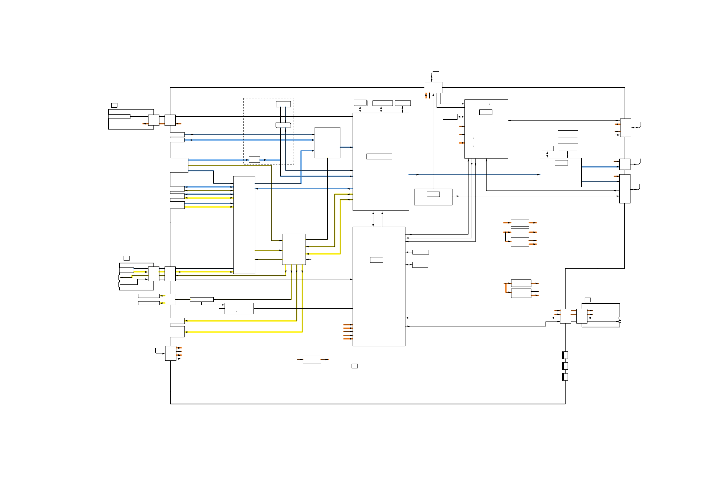
9 Block Diagram
9.1. Block (1 of 7) Diagram
SD CARD SLOT
GS
SD CARD I/F
HEADPHONE
+3.3V(S)
FRONT TERMINAL
G
AV3
KEY
Y,C , V
L,R
SPEAKER(R)
SPEAKER(L)
GS52
G51
from
P5
A52
A51
A12
A7
HDMI1
HDMI2
Dig/Ana
Tuner
AV1
AV2
COMP
MONITOR
OUT
DIGITAL
AUDIO
OUT
+3.3V(S)
Y,C , V
L,R
Y,C , V
L,R
Y,PB,PR
L,R
Y,C , V
L,R
HP L/R
KEY SCAN
+15V(SOUND)
+5V(STB)
+15V(F_STB)
ALL OFF
IFD1/2
SIF,AM
RF
AUDIO AMP
SOUND+15V
VIDEO
AUDIO
SWITCH
SOUND SOS DET
B/E ONLY
OFDM
L,R
L,R
(ATV or DTV)
SOUND_SOS
CI SLOT
BUFFER
HP
PWM
MONITOR L,R
OPT
AUDIO
PROCESSOR
BT+30V
HDMI
DTV
IECOUT
RESET
HDMI Rx
A/D CONV.
+30V(BT)+9V(P)
+9V(S)
+9V(M)
+5V(S)
+3.3V(M)
+3.3V(S)
DDR2
CLOCK GEN
SD DATA
Digital Video Signal
Peaks Lite2p
(MAIN MPU+VIDEO PROCESSOR)
HSDIN
TS Parallel
Digital
DVB_CVBS
DTV
IEC OUT
SERIAL
SBO2
SBI2
SD BOOT
PANEL_STB_ON
PANEL SIDE SOS
PANEL_STATUS
STANDBY MPU
GenX5
KEY1
SOUND SOS
(LED 11TIMES)(LED 12TIMES)
REMOTE
DTV+9V SENSE
MAIN+9V SENSE
SUB+5V SENSE
MAIN+3.3V SENSE
SUB+5V SENSE
R_LED_ON
G_LED_ON
DIGITAL MAINA
EEPROM
LVDS
RESET
IIC1
Dischrge Control
RESET
EEPROM
+5V(P)
A20
+15V(P)
FPGA
to/from
SC20
SOS6_SC1
SOS7_SC2
EEPROM
+15V(P)
SCAN CONTROL
+3.3V(P)
LVDS
+15V(P) DET
(LED
+3.3V(P) DET MAIN ON/OFF
(LED
+5V(P) DET
+5V(P)
(LED
Ready,ALARM
PANEL STB_ON
2TIMES)
3TIMES)
5TIMES)
(LED
PANEL STATUS
(LED
(LED
Genx6
MPU
(LED 4TIMES)
SOS8_SS
8TIMES)
6TIMES)
7TIMES)
POWER_SOS
+5V(STB)
+15V(P)
+15V(S)
DCDC
+3.3VSTB)
DCDC
+2.5V(P)
DCDC
+3.3V(P)
+1.2V(P)
DCDC
SUB+3.3V
DCDC
SUB+1.2V
SUB+1.8V
DDR
LVDS Rx
CPG with SS
H/V Sync Control
Sub Filed Processor
Plasma AI
+3.3V(STB)
+2.5V(P)
+3.3V(P)
+1.2V(P)
+3.3V(S)
+1.2V(S)
+1.8V(S)
+3.3V(STB)
+5V(S)
PD2-M
A33
A34
Thermal
sensor
FLASH
MEMORY
A1
FOR FACTORY USE
FOR FACTORY USE
SUSTAIN CONTROL
K
K1
POWER SOS
VIDEO DATA
VIDEO DATA
SOS8_SS
LED/RMT
+3.3V(STB)
+5V(S)
+5V(P)
+15V(P)
+5V(P)
+5V(P)
A25
A31
A32
REMOTE
LED
to/from
P25
to/from
C21
to
C11
TH-37/42PV8P, PX8B/E
Block (1/7) Diagram
27
A35
FOR FACTORY USE
TH-37/42PV8P, PX8B/E
Block (1/7) Diagram
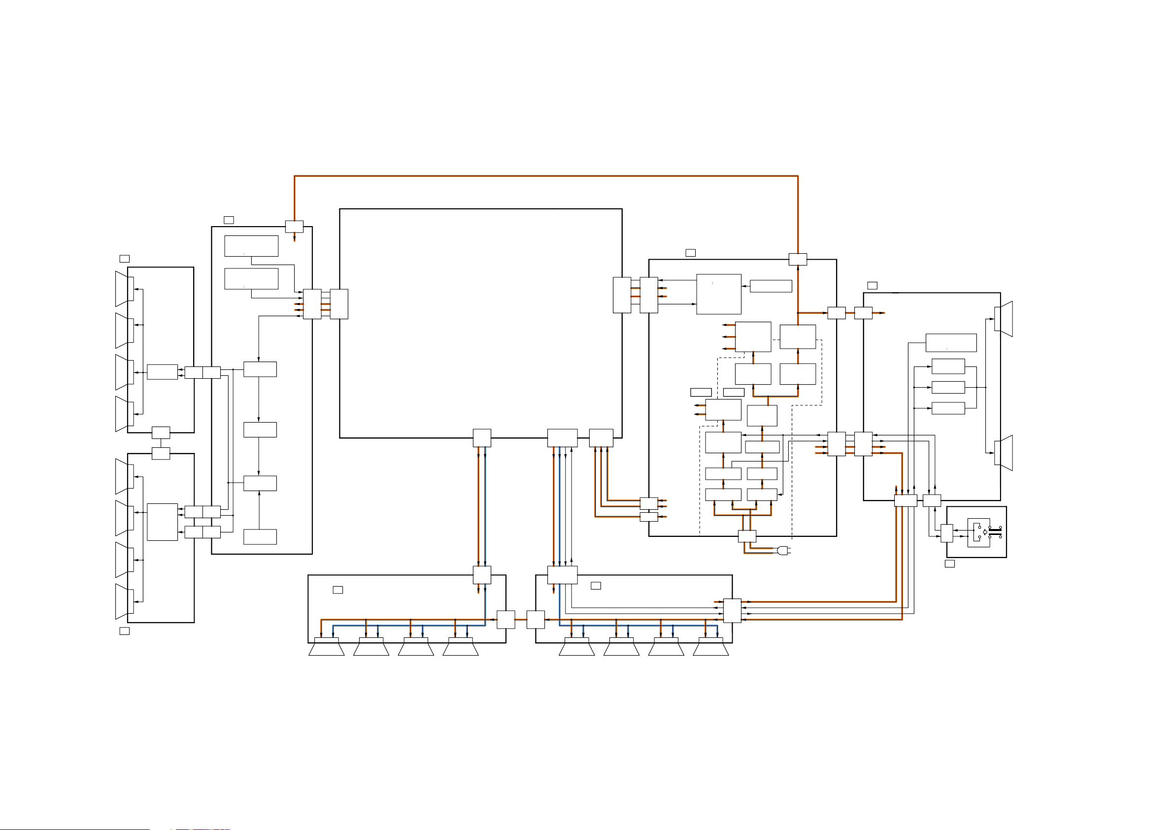
9.2. Block (2 of 7) Diagram (42 inch)
SU SCAN OUT (UPPER)
SCAN
DRIVER
SU11
SD11
SCAN
DRIVER
SCAN OUT (LOWER)SD
SU41
SD42
SD46
SC41
SC42
SC46
SC SCAN DRIVE
SC-BOARD
ENEGRY RECOVERY
SOS DETECT
(LED
6 TIMES)
SC-BOARD
FLOTING PART
SOS DETECT
7 TIMES)
(LED
CONTROL
PULSE
SUSTAIN
PULSE
SCAN
PULSE
VOLTAGE
GENERATOR
SC2
VSUS
SOS6_SC1
SOS7_SC2
+5V(P)
+15V(P)
SCAN CONTROL
SC20
DATA
DRIVER
A20
DATA DRIVER (RIGHT)
C1
DATA
DRIVER
Main Block(Tuner side)
A31
C11
+5V(P)
VIDEO DATA
C10
DATA
DRIVER
DATA
DRIVER
POWER SUPPLY
P
PS SOS
(LED
+5V(P)
+15V(P)
P25
A25
F+15V
+5V(STB)
SOS8_SS
VdaVda
A7
DATA DRIVER (LEFT)
C2
DATA
DRIVER
F+15V
P6
+15V(SND)
+5V(STB)
P7
DATA
DRIVER
A32
C21
+5V(P)
C20
VIDEO DATA
DATA
DRIVER
4 TIME)
POWER MICOM
ON/OFF CONTROL
Vda
+15V(P)
+5V(P)
COLD HOT
STANBY
VOLTAGE
RECTIFIER
STANBY
VOLTAGE
CONTROL
RECTIFIER
LINE
FILTER
+5V(P)
DATA
DRIVER
C23
PROCESS
VOLTAGE
RECTIFIER
PROCESS
VOLTAGE
CONTROL
POWER
FACTOR
CONTROL
RECTIFIER
P9
P-BOARD
SOS DETECT
LINE
FILTER
RELAY
+5V(P)
SOS8_SS
SUSTAIN CONTROLSUSTAIN CONTROL
Vda
P2
VSUS
SUSTAIN
VOLTAGE
RECTIFIER
SUSTAIN
VOLTAGE
CONTROL
MAIN SW2
MAIN SW1
+15V(P)
AC CORD
SUSTAIN DRIVESS
VSUS
P11
P12
Vda
SS11
SS12
VSUS
MAIN SW2
MAIN SW1
+15V(P)
+5V(P)
Vda
SS23
SOS8_SS
SUSTAIN CONTROL
SS-BOARD
SOS DETECT
(LED
ADDRESS
VOLTAGE
(VE)
SUSTAIN
PULSE
MAIN SW1
MAIN SW2
SS34
ERASE
PULSE
S1
8 TIME)
POWER SW
POWER SWITCH
S
ON
TH-42PV8P, PX8B/E
Block (2/7) Diagram
TH-42PV8P, PX8B/E
Block (2/7) Diagram
28
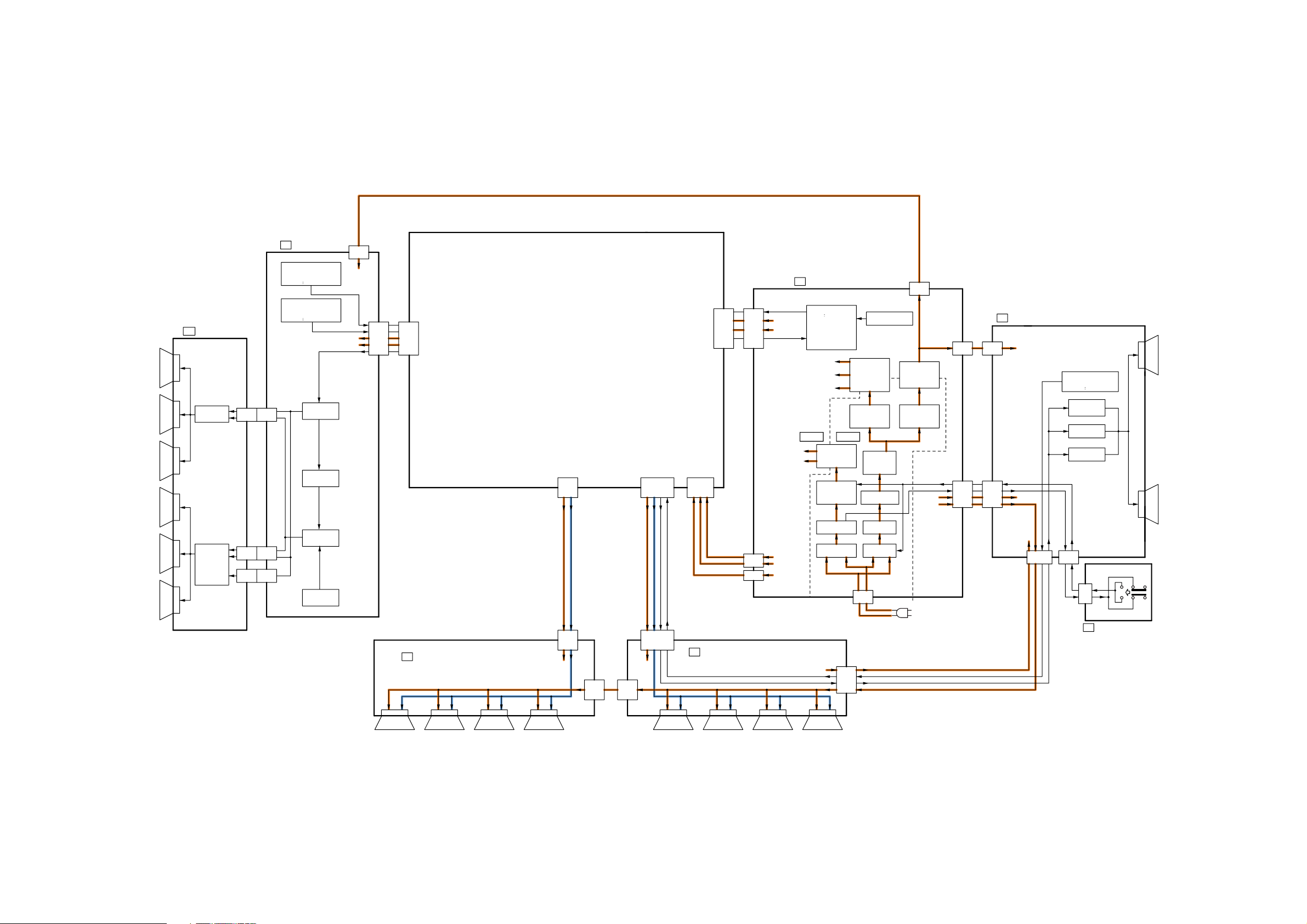
9.3. Block (3 of 7) Diagram (37 inch)
SM SCAN OUT
SCAN
DRIVER
SCAN
DRIVER
SC41
SM41
SM42
SC42
SM46 SC46
SC SCAN DRIVE
SC-BOARD
ENEGRY RECOVERY
SOS DETECT
6 TIMES)
(LED
SC-BOARD
FLOTING PART
SOS DETECT
7 TIMES)
(LED
CONTROL
PULSE
SUSTAIN
PULSE
SCAN
PULSE
VOLTAGE
GENERATOR
SC2
VSUS
SOS6_SC1
SOS7_SC2
+5V(P)
+15V(P)
SCAN CONTROL
SC20
A20
DATA DRIVER (RIGHT)
C1
Main Block(Tuner side)
A31
C11
+5V(P)
VIDEO DATA
Vda
C10
POWER SUPPLY
P
PS SOS
(LED
+5V(P)
+15V(P)
P25
A5
F+15V
+5V(STB)
A32
C21
+5V(P)
C20
VIDEO DATA
A7
DATA DRIVER (LEFT)
C2
SOS8_SS
SUSTAIN CONTROL
Vda
F+15V
P6
+15V(SND)
+5V(STB)
P7
4 TIME)
POWER MICOM
ON/OFF CONTROL
Vda
+15V(P)
+5V(P)
COLD HOT
STANBY
VOLTAGE
RECTIFIER
STANBY
VOLTAGE
CONTROL
RECTIFIER
LINE
FILTER
+5V(P)
C23
PROCESS
VOLTAGE
RECTIFIER
PROCESS
VOLTAGE
CONTROL
POWER
FACTOR
CONTROL
RECTIFIER
LINE
FILTER
RELAY
P9
+5V(P)
SOS8_SS
SUSTAIN CONTROL
Vda
P-BOARD
SOS DETECT
P2
VSUS
SUSTAIN
VOLTAGE
RECTIFIER
SUSTAIN
VOLTAGE
CONTROL
MAIN SW2
MAIN SW1
+15V(P)
AC CORD
SUSTAIN DRIVESS
VSUS
P11
P12
Vda
SS11
SS12
VSUS
MAIN SW2
MAIN SW1
+15V(P)
+5V(P)
SS23
Vda
SOS8_SS
SUSTAIN CONTROL
SS-BOARD
SOS DETECT
(LED 8 TIME)
ADDRESS
VOLTAGE
(VE)
SUSTAIN
PULSE
ERASE
PULSE
MAIN SW1
MAIN SW2
SS34
S1
POWER SWITCH
S
POWER SW
ON
TH-37PV8P, PX8B/E
Block (3/7) Diagram
DATA
DRIVER
DATA
DRIVER
DATA
DRIVER
DATA
DRIVER
DATA
DRIVER
29
DATA
DRIVER
DATA
DRIVER
DATA
DRIVER
TH-37PV8P, PX8B/E
Block (3/7) Diagram
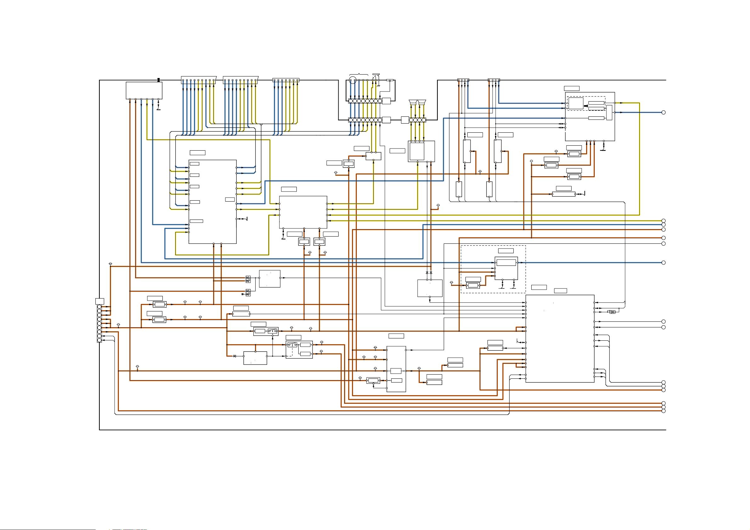
9.4. Block (4 of 7) Diagram
+15V_S
+15V_S
+15V_S
F+15V
F+15V
F+15V
STB5V
TUNER_SUB_ON
ECO_ON
P7
A7
13
15
17
10
12
14
A-BOARD
S_15V
1
2
3
F15V
Dig/Ana
Tuner
BT+30V
STB5V
TU8301
SUB+5V
IFD1/2
SIF,AM
IC5401
IC5400
RF
IIC_TUNER
+9V
+5V
SUB+9V
SUB+5V
JK3002
AV1_V
DTV9V
SUB5V
AV1
AV1_RED
AV1_GREEN
AV1_BLUE
AV1_LIN
IC3001
AV SW
AV1
V,R,G,B
L,R
AV2
V,Y,C,R,G,B
L,R
AV3
V,Y, C
L,R
COMP
Y,PB,PR
L,R
TV/DTV
RF
DVB_CVBS
L,R
MAIN9V
MAIN5V
AV1_RIN
AV1_VOUT
AV1_LOUT
AV1_ROUT
+9V +5V
JK3003
AV2_V_Y
AV1_VOUT
AV2_VOUT
AV1_L,ROUT
AV2_L,ROUT
L,ROUT
MAIN
CVBS/S/YUV
/RGB(PC)
AV2
AV2_RED_C
AV2_GREEN
L,R
D5612
(+5.6V)
AV2_BLUE
SUB+5V
DTV+9V
BT+30V
IC5660
RESET
AV2_LIN
AV2_RIN
IIC2
D5522
D5521
AV2_ROUT
AV2_VOUT
AV2_LOUT
XRST
IC5600
+3.3V
Q5606,07
F+15V DET
Norm Low
Ab
high
JK3100
Norm Low
high
Ab
SHOTO SOS
Q5522
(LED 3TIMES)
SUB+3.3V
AUDIO
YPBPR
IN/OUT
LIN
RIN
Y
PB
PR
IC2106
AUDIO PROCESSOR
SIF,AM
L,R
TV_LR/DTV_LR
IC2008
IIC2
SUB3.3V
IC5601
LOUT
HEADPHONE
AV3
ROUT
AV3_Y
10 15
AV3_C
AV3_V
6
415210 139326
AV3_L
4
IC2012
IC2013
+5V
MAIN9V
HEADPHONE
+3.3V
HP L,R
SP L,R
+1.8V
PWM
HDMI Audio
DTV
AV3_R
HP AMP
HP_L
9
HP_R
CONTROL
BUTTON
G51
KEY1
1
A51
IC2301
AUDIO AMP
SPEAKER L,R
A12
2
1
R(-)
R(+)
SPEAKER
OUT
3
4
L(+)
L(-)
SOS DET
+15V
SOUND15V
IC2107
+1.8V
+3.3V
SUB3.3VSUB5V
D2014
D2017
SOS Low
SOUND SOS
Q2022
(LED
12TIMES)
MAIN3.3V
+1.8V
+1.2V
SUB1.8V
SUB1.2V
BT30V
MAIN9V
Q2027
BT30V
SUB5V
DTV9V
STB5V
IC2403
STB3.3V
STB_RESET
STB_RST
STB
+3.3V
+9V
STB3.3V
IC1102
BUFFER
HDMI_CEC
SUB3.3V
IC4811
IIC SW
JK4500
Q4502
HDMI2
CEC
+5V
DDC IIC
DET2
+5V(HDMI)
B/E ONLY
TMDS
IC4515
5V<->3.3V
LEVEL SHIFT
DDC_IIC1
IC8302
+1.8V
STB5V
JK4501
Q4503
HDMI1
CEC
+5V
DET1
+5V(HDMI)
IC1101
EEPROM
TMDS
DDC IIC
IC4514
5V<->3.3V
LEVEL SHIFT
DDC_IIC0
IC8301
OFDM
DIGITAL
DEMODULATOR
XRST
3.3V
1.8V
IIC2
IIC_TUNER
IIC3
Analog video signal
SUB3.3V
IC1100
STANDBY_MPU
SOUND_SOS
KEY1
SOS
(LED 10TIMES)
XRST
STB_RST
MAIN3.3V_SENSE
SUB3.3V_SENSE
IIC3
IIC
STB+3.3V
SUB5V_SENSE
DTV_9V_SENSE
MAIN9V_SENSE
TUNER_SUB_ON
ECO_ON
HDMI1
HDMI2
(LED
IC4512
+1.8V
SUB5V
IC4800
TEMP SENSOR
GenX5
12TIMES)
IC4510
HDMI PROCESSOR
HDMI
DECORD
DDCB_IIC
DDCC_IIC
IC4511
+3.3V
IC4513
+1.8V
+5V(HDMI)
DET1,2,3
HDMI_CEC
HDMI_CEC_PU_ON
SD BOOT
PANEL SOS
(ARARM)
PANEL STB_ON
PANEL STATUS
(READY)
G_LED_ON
R_LED_ON
HDMI Rx/AD CONV.
AUDIO
VIDEO
A/D
+3.3V
+1.8V
+1.8V
IIC1
IIC1
SBI2
SBO2
RMIN
SW
D1107
Digtal
Audio
Signal
Digtal
Video
Signal
1
2
3
4
5
6
7
8
9
10
11
12
TH-37/42PV8P, PX8B/E
Block (4/7) Diagram
30
13
14
15
TH-37/42PV8P, PX8B/E
Block (4/7) Diagram
 Loading...