

Panasonic GP4D, TH-37PW4, TH-37PWD4 Service Manual
A
A
Specifications
ORDER NO. ITD0109010C0
D10
Wide Plasma Display
TH-37PW4
TH-37PWD4
GP4D Chassis
Power Source:
Power Consumption: 395 W (US model)
Plasma Display panel: Drive method AC type
Contrast Ratio 3000:1
Brightness Capability (Panel only) 650 cd / m
Screen size: 818 mm (W)×461 mm (H)×939 mm
Operating condition:
Temperature 34 °F - 104 °F (0 °C - 40 °C)
Humidity 20 % - 80 %
Applicable signals:
Color System NTSC, PAL, PAL60, SECAM, Modified NTSC
Scanning format 525i (480i), 625i (575i), 525p (480p), 625
PC signals VGA display
C120V 50/60Hz (US model)
C220-240V 50/60Hz (Except US model)
295W (Except US model)
1.2W (stand-by condition) (US model)
1.8W (stand-by condition)
(Except US model)
0.9W (Power off condition) (US model)
1.6W (Power off condition)
(Expct US model)
37-inch, 16:9 aspect ratio
2
(As a set) 330 cd / m
(diagonal)
No. of pixels
408,960 (852 (W)×480 (H)) [2,556×480 dots]
(575p), 750p (720p), 1125/60i, 50i, 24p, 24SF
(1080/60i, 50i, 24p, 24SF) ........SMPTE 274M
VGA
SVGA, SXGA, UXGA ...... (compressed)
Horizontal scanning frequency 15.5 - 110kHz
2
Vertical scanning frequency 48 - 120Hz
Connection terminals:
AV
Video in 1.0 Vp-p (75-ohm)
S-VIDEO IN
(MINI DIN 4PIN)
AUDIO IN
(RCA PIN JACK × 2)
COMPONENT/RGB
Y/G 1.0 Vp-p/composite (75-ohm)
PB/B 0.7 Vp-p (75-ohm)
PR/R 0.7 Vp-p (75-ohm)
HD 1.0 - 5.0 Vp-p (high impedance)
VD 1.0 - 5.0 Vp-p (high impedance)
AUDIO IN
(RCA PIN JACK×2)
PC
(HIGH-DENSITY
D-SUB15PIN)
AUDIO IN (M3.5 JACK) 0.5Vrms (high impedance)
SERIAL
EXTERNAL CONTROL
TERMINAL (D-SUB9PIN)
SPEAKERS (External
speakers)
Dimensions (W×H×D): 36.2” (920 mm)21.7” (550mm) 3.5” (89 mm)
Weight (Mass) approx. 55.1 Ibs (25.0 kg) (main unit only)
Y: 1 Vp-p (75-ohm), C: 0.286 Vp-p
(75-ohm)
0.5 Vrms (high impedance)
0.7 Vp-p/non-composite (75-ohm)
0.5 Vrms (high impedance)
R,G,B/0.7 Vp-p (75-ohm)
HD, VD/1.0 - 5.0 Vp-p (high
impedance)
RS-232C COMPATIBLE
69 8W×2 (10% THD)
approx. 64.4 Ibs (29.2kg) (with speakers)
© 2001 Matsushita Electric Industrial Co., Ltd. All
rights reserved. Unauthorized copying and
distribution is a violation of law.
TH-37PW4 / TH-37PWD4
CONTENTS
Page Page
1 Safety Precautions 4
1.1. General Guidelines
2 Prevention of Electro Static Discharge (ESD) to
Electrostatically Sensitive (ES) Devices
3 PCB Structure sheet of GP4D chassis
4 Service Hint
5 Location of Lead Wiring
6 Adjustment Procedure
6.1. +B Set-up
6.2. Driver Set-up
6.3. Initialization Pulse Adjust
6.4. P.C.B. (Printed Circuit Board) exchange
6.5. Adjustment Volume Location
6.6. Test Point Location
7 Serviceman mode
7.1. CAT (computer Aided Test) mode
7.2. IIC mode structure (following items value is sample data.)
8 Alignment
8.1. NTSC panel white balance
8.2. PAL/SECAM panel white balance
8.3. Pedestal setting
8.4. PC/RGB panel white balance
8.5. HD/ 525i /525p panel white balance
8.6. 625i panel balance
8.7. Sub brighness setting
9 Trouble shooting guide
9.1. Self Check
9.2. No Power (US model)
9.3. No Power (Except US)
9.4. No Picture
9.5. Local screen failure
9.6. D-Board
10 Option Setting
11 IC Block Diagram
12 Conductor Views
12.1. F-Board
12.2. P-Board (US model)
12.3. P1-Board (Except US)
12.4. P3, P5, P6, P7 and P8-Board (Except US)
12.5. HX-Board
12.6. HZ-Board (Option TY-37TM4Z)
12.7. J-Board
12.8. D-Board
12.9. C1, C2, C3 and C4-Board
10
11
11
11
12
12
14
15
15
16
18
19
21
23
24
26
26
27
28
29
29
30
32
35
37
37
38
41
44
46
47
49
51
54
4
5
6
7
8
9
9
9
12.10. SC-Board
12.11. SU and SD-Board
12.12. SS, SS2 and SS3-Board
12.13. H3, S1 and V1-Board
13 Block and Schematic Diagrams
13.1. Schematic Diagram Notes
13.2. Main Block (US model) Diagrams
13.3. Main (Except US) Block Diagram
13.4. Power (US model) Block Diagram
13.5. P-Board (US model) Schematic Diagrams
13.6. Power (Except US) Block Diagram
13.7. P1-Board (Except US) Schematic Diagrams
13.8. F and P3-Board (Except US) Schematic Diagram
13.9. P5, P6, P7 and P8-Board (Except US) Schematic diagram
13.10. HX and H Block Diagram
13.11. HX-Board Schematic Diagrams
13.12. H-Board (Option TY-42TM4H) Schematic Diagram
13.13. HZ Block Diagrams
13.14. HZ-Board (1/2) (Option TY-37TM4Z) Schematic Diagram
13.15. HZ-Board (2/2) (Option TY-37TM4Z) Schematic Diagram
13.16. J-Board Block Diagrams
13.17. J-Board (1/5) Schematic Diagrams
13.18. J-Board (2/5) Schematic Diagrams
13.19. J-Board (3/5) and H3-Board Schematic Diagrams
13.20. J-Board (4/5) Schematic Diagrams
13.21. J-Board (5/5) Schematic Diagrams
13.22. D-Block Diagrams
13.23. D-Board (1/14) Schematic Diagrams
13.24. D-Board (2/14) Schematic Diagrams
13.25. D-Board (3/14) Schematic Diagrams
13.26. D-Board (4/14) Schematic Diagrams
13.27. D-Board (5/14) Schematic Diagrams
13.28. D-Board (6/14) Schematic Diagrams
13.29. D-Board (7/14) Schematic Diagrams
13.30. D-Board (8/14) Schematic Diagrams
13.31. D-Board (9/14) Schematic Diagrams
13.32. D-Board (10/14) Schematic Diagrams
13.33. D-Board (11/14) Schematic Diagrams
13.34. D-Board (12/14) Schematic Diagrams
13.35. D-Board (13/14) Schematic Diagrams
13.36. D-Board (14/14) Schematic Diagrams
13.37. C1-Board Schematic Diagrams
56
59
61
64
65
65
66
67
68
69
70
71
72
73
74
75
76
77
78
79
80
81
82
83
84
85
86
87
88
89
90
91
92
93
95
96
97
98
99
100
101
102
2

13.38. C2-Board Schematic Diagrams 103
13.39. C3-Board Schematic Diagrams
13.40. C4-Board Schematic Diagrams
13.41. SC-Board Block Diagrams
13.42. SC-Board (1/2) Schematic Diagrams
13.43. SC-Board (2/2) Schematic Diagrams
13.44. SU/SD Block Diagram
13.45. SU-Board Schematic Diagrams
13.46. SD-Board Schematic Diagrams
13.47. SS-Board Block Diagrams
104
105
106
107
108
109
110
111
112
TH-37PW4 / TH-37PWD4
13.48. SS, SS4, SS5 and S1-Board Schematic Diagrams 113
14 Parts Location
15 Mech anica l Replacement Parts List
15.1. US model
15.2. Except US model
16 Repla ceme nt Parts List
16.1. Relpacement Parts List Notes
16.2. US model Electrical Replacement Parts List
16.3. Expect US model Electrical Replacement Parts List
16.4. Option (TY-37TM4Z) Replacement Parts List
115
117
117
117
120
120
121
140
161
3
TH-37PW4 / TH-37PWD4
1 Safety Precautions
1.1. General Guidelines
1. When servicing, observe the original lead dress. If a short circuit is found, replace all parts which have been overheated or
damaged by the short circuit.
2. After servicing, see to it that all the protective devices such as insulation barriers, insulation papers shields are properly
installed.
3. After servicing, make the following leakage current checks to prevent the customer from being exposed to shock hazards.
1.1.1. Leakage Current Cold Check
1. Unplug the AC cord and connect a jumper between the two
prongs on the plug.
2. Measure the resistance value, with an ohmmeter, between
the jumpered AC plug and each exposed metallic cabinet
part on the equipment such as screwheads, connectors,
control shafts, etc. When the exposed metallic part has a
return path to the chassis, the reading should be between
1M9 and 5.2M9.
When the exposed metal does not have a return path to
the chassis, the reading must be
.
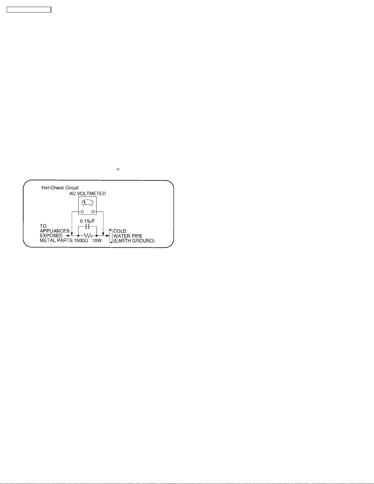
Figure 1
1.1.2. Leakage Current Hot Check (See
Figure 1.)
1. Plug the AC cord directly into the AC outlet. Do not use an
isolation transformer for this check.
2. Connect a 1.5k9, 10 watts resistor, in parallel with a 0.15µF
capacitors, between each exposed metallic part on the set
and a good earth ground such as a water pipe, as shown in
Figure 1.
3. Use an AC voltmeter, with 1000 ohms/volt or more
sensitivity, to measure the potential across the resistor.
4. Check each exposed metallic part, and measure the
voltage at each point.
5. Reverse the ACplugintheACoutletandrepeat each of the
above measurements.
6. The potential at any point should not exceed 0.75 volts
RMS. A leakage current tester (Simpson Model 229 or
equivalent) may be used to make the hot checks, leakage
current must not exceed 1/2 milliamp. In case a
measurement is outside of the limits specified, there is a
possibility of a shock hazard, and the equipment should be
repaired and rechecked before it is returned to the
customer.
4
TH-37PW4 / TH-37PWD4
2 Prevention of Electro Static Discharge (ESD) to
Electrostatically Sensitive (ES) Devices
Some semiconductor (solid state) devices can be damaged easily by static electricity. Such components commonly are called
Electrostatically Sensitive (ES) Devices. Examples of typical ES devices are integrated circuits and some field-effect transistors and
semiconductor "chip" components. The following techniques should be used to help reduce the incidence of component damage
caused by electro static discharge (ESD).
1. Immediately before handling any semiconductor component or semiconductor-equipped assembly, drain off any ESD on your
body by touching a known earth ground. Alternatively, obtain and wear a commercially available discharging ESD wrist strap,
which should be removed for potential shock reasons prior to applying power to the unit under test.
2. After removing an electrical assembly equipped with ES devices, place the assembly on a conductive surface such as alminum
foil, to prevent electrostatic charge buildup or exposure of the assembly.
3. Use only a grounded-tip soldering iron to solder or unsolder ES devices.
4. Use only an anti-static solder removal device. Some solder removal devices not classified as "anti-static (ESD protected)" can
generate electrical charge sufficient to damage ES devices.
5. Do not use freon-propelled chemicals. These can generate electrical charges sufficient to damage ES devices.
6. Do not remove a replacement ES device from its protective package until immediately before you are ready to install it. (Most
replacement ES devices are packaged with leads electrically shorted together by conductive foam, alminum foil or comparable
conductive material).
7. Immediately before removing the protective material from the leads of a replacement ES device, touch the protective material
to the chassis or circuit assembly into which the device will be installed.
Caution
Be sure no power is applied to the chassis or circuit, and observe all other safety precautions.
8. Minimize bodily motions when handling unpackaged replacement ES devices. (Otherwise hamless motion such asthe brushing
together of your clothes fabric or the lifting of your foot from a carpeted floor can generate static electricity (ESD) sufficient to
damage an ES device).
5
TH-37PW4 / TH-37PWD4
3 PCB Structure sheet of GP4D chassis
Board Name US model Except US model Function Remarks
P3 --- TNP1777 Drive voltage oscillator
P5 --- TNP1778 Primary oscillator
P6 --- TNP1779 PFC oscillator
P7 --- TNPA1780 Drive voltage protection
P8 --- TNPA1781 Process voltage protection
P1 --- TXNP11JASE Power Supply 1
P TXN/P10JAS --- Power Supply 1
F TXN/F10JAS TXN/F1JASE Line Filter 1
V1 TNPA2282 Front SW & Remote receiver
S1 TNPA2283 Power SW
HX TZTNP010JBS PC type Input terminal
HZ TZTNP020JBS RCA type Input terminal
H3 TNPA2249 Speaker terminal
SC TNPA2261 Scan Drive
D TZTNP01JCSE Digital process & control 1, 2
J TNPA2244 Separator / Audio Out 1
C1 TNPA2278 Data Drive (Upper Left)
C2 TNPA2279 Data Drive (Upper Right)
C3 TNPA2280 Data Drive (Lower Left)
C4 TNPA2281 Data Drive (Lower Right)
SU TNPA2284 Scan Out (Upper) 1
SD TNPA2285 Scan Out (Lower) 1
SS TNPA2262AB Sustain Drive 1
SS4 TNPA2377 Sustain Connection (Upper)
SS5 TNPA2278 Sustain Connection (Lower)
Remarks
1. Recommend PCB´s for initial service for GP4D chassis.
2. Parts number of System model is TZTNP01JASE
Note
US model TH-37PWD4UZ
Except US model TH-37PW4AZ/BX/EX/HZ/RZ
TH-37PWD4AZ/BX/EX/HZ/RZ
6
4 Service Hint
TH-37PW4 / TH-37PWD4
7
TH-37PW4 / TH-37PWD4
5 Location of Lead Wiring
8
6 Adjustment Procedure
TH-37PW4 / TH-37PWD4
6.1. +B Set-up
6.1.1. Item / Preparation
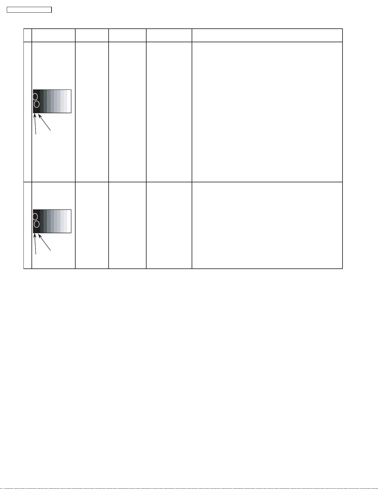
1. Input a Grey scale signal.
2. Set the picture controls: Picture mode: Normal
White balance: Normal
6.1.2. Adjustments
Adjust and confirm indicated test point for the specified voltage.
Adjust
Test point Voltage Volume Name
P4 pin 1 (Hot) 400V ±1V R426 (P1)
Except US
P1 pin 3 170V ±1V R476 (P) US model Vsus
R625 (P3)
Expect US
P2 pin 3 160V ±1V R505 (P) US model Vbk
R498 (P1)
Except US
P12 pin 1 67V ±0.5V R473 (P) US model Vda
R519 (P1)
Except US
Confirm
Test point Voltage Volume Name
P23 pin 2 15V ±0.5V +15V
P5 pin 1 13.5V ±0.5V +13V
P13 pin 1 13.5V ±0.5V Audio 15V
P13 pin 3 -13.5V ±0.5V Audio -15V
P5 pin 5 5.1V ±0.3V 5V
P7 pin4 5V ±0.2V STB5V (1)
P14 pin 8 5.0V ±0.3V STB5V (2)
P10 pin 1 17.0V ±0.5V FAN +B
P10 pin 4 5.1V ±0.3V FAN 5V
PFC
6.2. Driver Set-up
6.2.1. Item / Preparation
1. Input an APL 100 % white signal.
2. Set the picture controls: Picture mode: Normal
White balance: Cool
Aspect: 16:9
6.2.2. Adjustments
Adjust driver section voltages referring the panel data on the
panel data label.
Test point Voltage Volume Name
TPVSUS
(SS-BOARD)
TPVBK
(SC-BOARD)
TPVE
(SS-BOARD)
TPVSET
(SC-BOARD)
TPVAD
(SC-BOARD)
TPVDA
(SC-BOARD)
*See the Panel label.
Vsus ±1V* R478 (P) US model Vsus
R625 (P3)
Except US
Vbk ±1V* R505 (P) US model Vbk
R498 (P1)
Except US
Ve ± 1V* R6774 (SS) Ve
218 V ±6V --- Vset
Vad ±1V* R6477 (SC) Vad
67V±1V R473 (P) US model Vda
R519 (P1)
Except US
9
TH-37PW4 / TH-37PWD4
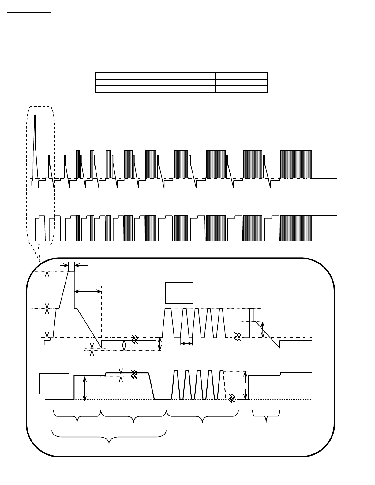
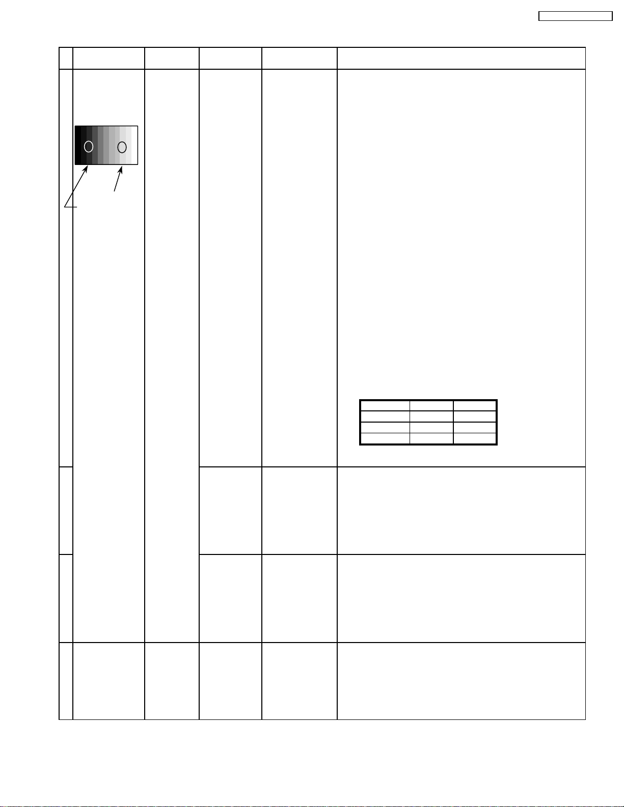
6.3. Initialization Pulse Adjust
1. Input a Cross hatch signal.
2. Set the picture controls: Picture mode: Normal
White balance: Cool
Adjust the indicated test point for the specified wave form.
Test point Volume Level
T1 TPSC1 (SC) R6523 (SC) 20 } 15µ Sec
T2 TPSC1 (SC) R6557 (SC) 170 } 20µ Sec
TPSC1 SCAN OUTPUT
TPSS1 SUSTAIN OUTPUT
T1 20±15µs
VSET
T2 170±20µs
Scan
TPSC1
VSUS VBK
VSCN VAD
VSET2
6µs
VSUS
Sustain
TPSS1
INITIALIZE SCAN PRE-INITIALIZE
VE
ADDRESS PERIOD
VE2
SUSTAIN
10
VSUS
6.4. P.C.B. (Printed Circuit Board) exchange
6.4.1. Caution
1. To remove P.C.B. , wait 1 minute after power was off for discharge from electrolysis capacitors.
6.4.2. Quick adjustment after P.C.B. exchange
P.C.B. Item Volume Test point Level
P board PFC R426 (3) Except US P4 connector pin 1 400V ± 1 V
Vsus R478 (P) US model TPVsus (SS) 175V ± 1 V
R625 (P3) Except US
Vbk R505 (P) US model TPVBK (SC) 160V ± 5 V
R498 (P1) Except US
Vda R473 (P) US model TPVDA (SS) 67V ± 1 V
R519 (P1) Except US
SC board Vad R6477 TPVAD (SC) -90 ± 1 V
SS board Ve R6774 TPVE (SS) 150 ± 1 V
D board White balance, Pedestal and Sub brightness for NTSC, PAL, HD, PC and 625I signals.
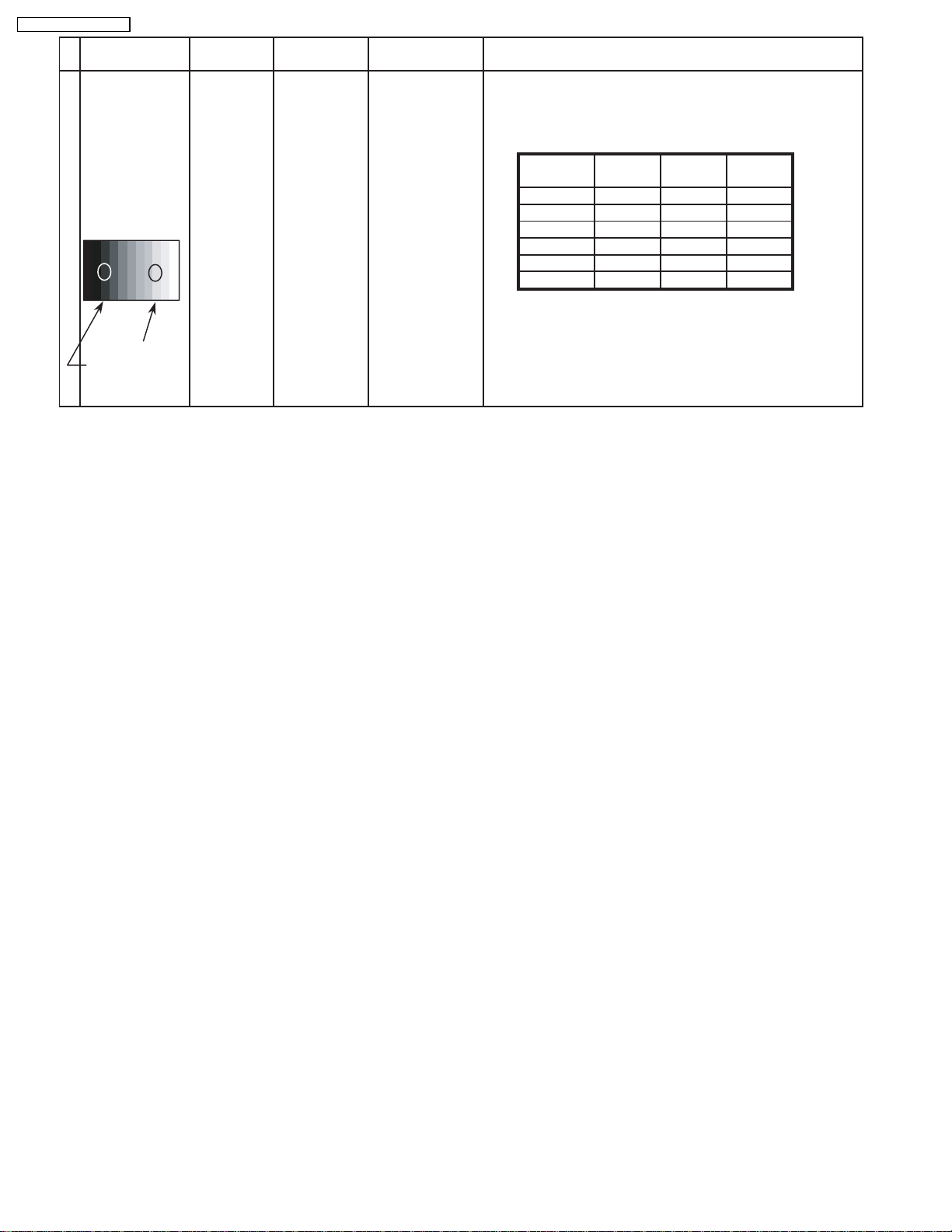
6.5. Adjustment Volume Location
TH-37PW4 / TH-37PWD4
6.6. Test Point Location
11
TH-37PW4 / TH-37PWD4
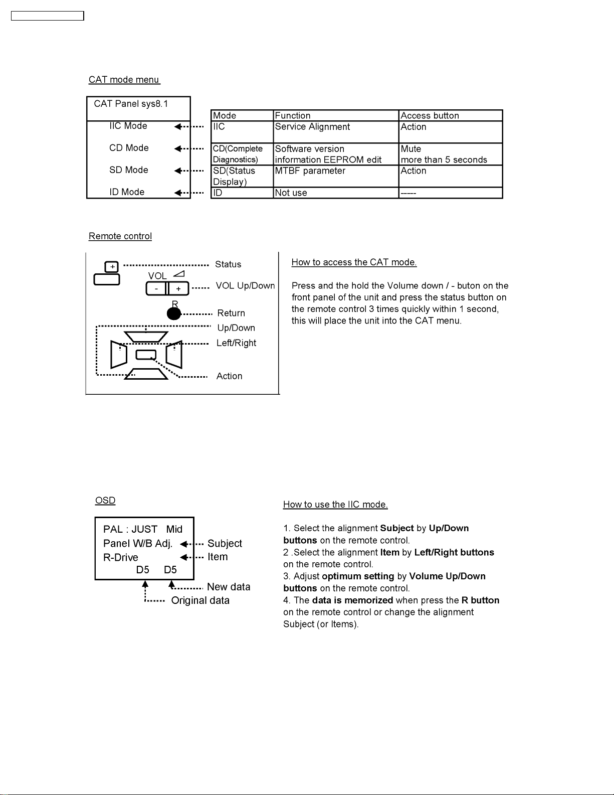
7 Serviceman mode
7.1. CAT (computer Aided Test) mode
To exit the CAT mode, access the ID mode and switch off the main power.
7.1.1. IIC mode
Select the IIC mode by Up/Down button on the remote control at the front page of CAT mode then press the Action button on
the remote control.
Subject and item are mentioned on page 14.
To exit the IIC mode, press the R button on the remote control.
12
TH-37PW4 / TH-37PWD4
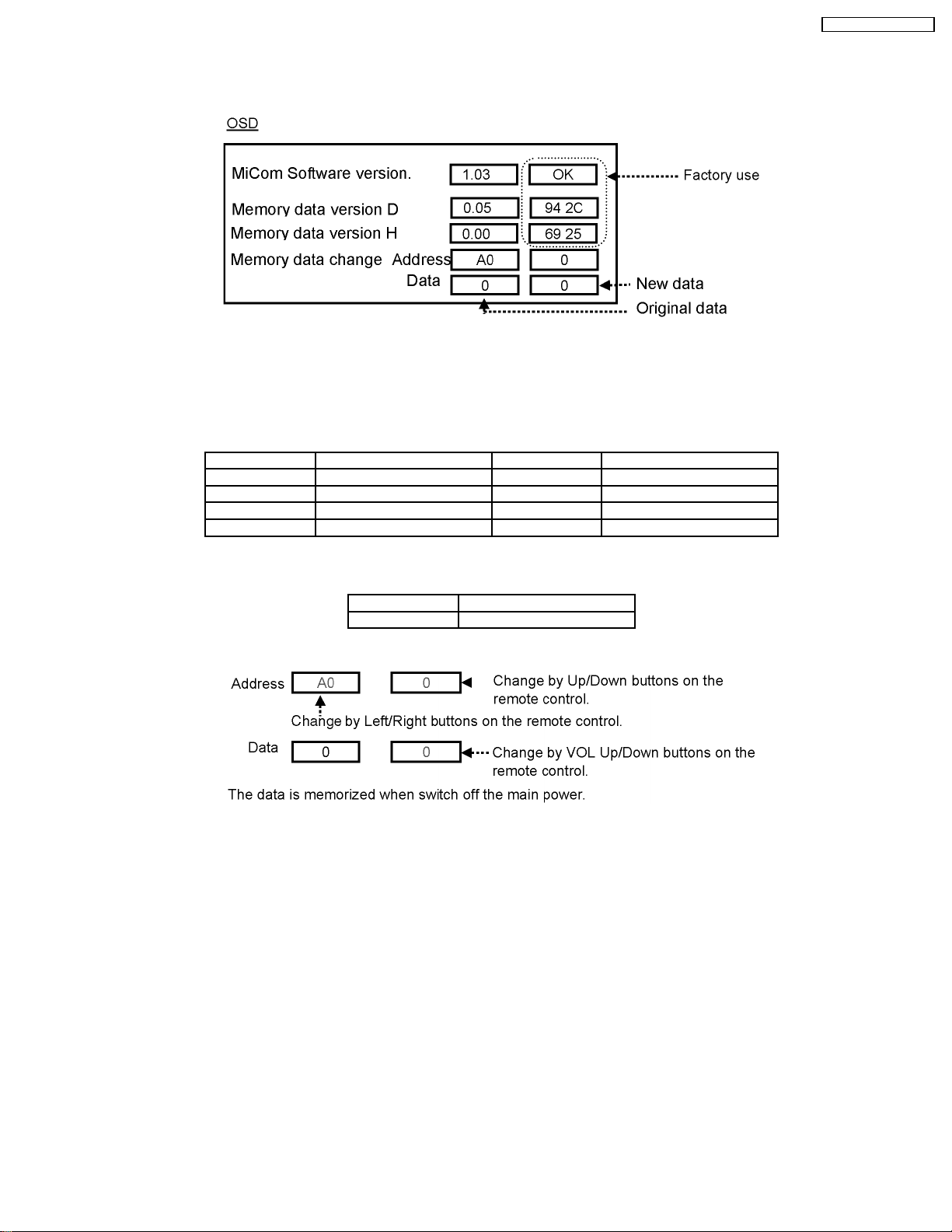
7.1.2. CD mode
Select the CD mode by Up/Down button on the remote control at the front page of CAT mode then press the Mute button on the
remote control more than 5 sec.
Micom software version ( IC9705 / TVRJ562), this version can be upgrade by
1. replace of new version IC
2. Loading the new version software from loader tool, TZSC07036.
Memory data version D (IC9706 /TVRJ601) in the D board
Version Model Type Destination
4.** PWD4UZ System USA
5.** PW4BX,HZ, Consumer U.K.H.K.,
6.** PWD4AY,BX, EX, HZ, RZ System U.K. / Euro / Australia
7.** PW4AZ, EX, RZ Consumer Euro / Australia
Memory data version H (IC3699) in the H board
This version is difference depends on the H board type.
Version Type of H borad
2.** HZ (RCA)
Memory data change
To exit the CD mode, press the R button on the remote control.
13
TH-37PW4 / TH-37PWD4
7.1.3. SD mode
Select the SD mode by Up/Down button on the remote control at the front page of CAT mode then press the Action button on the
remote control.
To exit the SD mode, press the R button on the remote control.
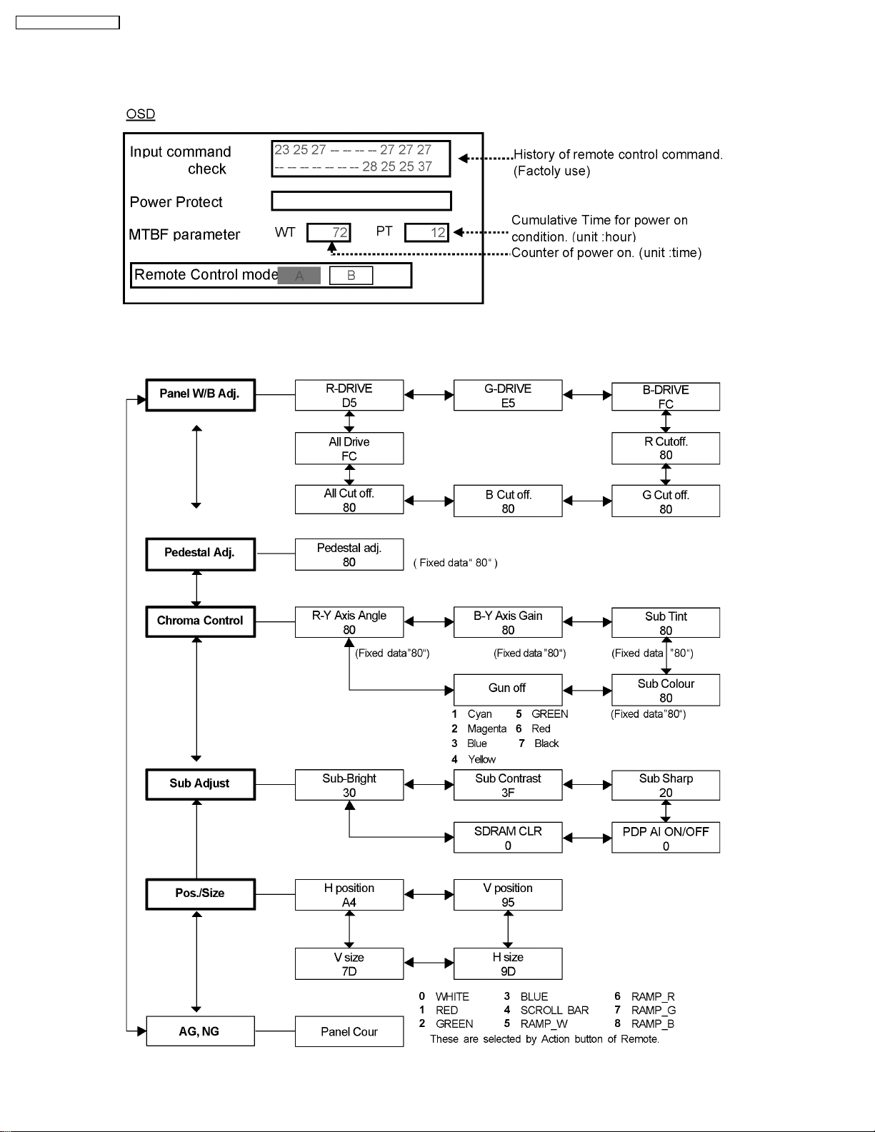
7.2. IIC mode structure (following items value is sample data.)
14
8 Alignment
8.1. NTSC panel white balance
INPUT Alignment menu ProcedureEquipment Setting
1 NTSC Color Picture: 1) Find the nearest area to brightness of 10 cd/m2 as Low
Gray Scale Analyzer Normal Sub Adjust light by color sensor.
Pattern White balance: Sub Bright 2) Adjust Sub bright to set Low light level to 10 cd/m
Cool
Aspect: PANEL W/B
16:9 G cut off 3) Set G cut off to " 80 ".
PANEL W/B
B cut off 4) Adjust B and R cut off to set color temperature as
R cut off shown Fig.-01.
High light 75% Sub Adjust
Low light 15% Sub Bright 5) If Sub Bright is changed re-adjust it to set Low light
PANEL W/B
PANEL W/B
exactly.
to 10 cd/m
6)Find 75% of white area by color sensor.
G Drive 7) Set G Drive to " D8 ".
B Drive 8) Adjust B and R Drive to set color temperature
R Drive as shown Fig.-01.
2
.
TH-37PW4 / TH-37PWD4
2
9) Repeat item 4) to 7) to set both Low light and
high light.
PANEL W/B
R,G,B Drive 10) Increase same steps of R, G and B Drive to set
R,G,B Drive largest level of 3 color drive to "FC".
PANEL W/B
R,G,B cut off 11) Re-adjust Low light level again.
Color Temp. x y
Cool(Hi) 0.272 0.290
Normal(Mid) 0.288 0.296
Warm(Low) 0.313 0.329
Fig. -01
2 Picture: 1) Change white balance to "Normal".
Normal PANEL W/B
White balance: R,G,B cut off 2) Repeat procedure 3) to 11) of Cool mode.
Normal
PANEL W/B
Aspect: R,G,B Drive
16:9
3 Picture: 1) Change white balance to "Warm".
Normal PANEL W/B
White balance: R,G,B cut off 2) Repeat procedure 3) to 11) of Cool mode.
Warm
PANEL W/B
Aspect: R,G,B Drive
16:9
4 Picture: Picture Menu 1) Change color templature to "Cool".
Normal Sub Adjust
White balance: Sub Bright 2)Re-set Sub bright to "30"
Cool
Aspect:
16:9
Note:
OSD is the difference between US model and Except US model.
Picture:Normal (Except US)/Standard (US model)
White balance (Except US)/Color Temp (US model)
15
TH-37PW4 / TH-37PWD4
8.2. PAL/SECAM panel white balance
INPUT Alignment menu ProcedureEquipment Setting
1 PAL Color Picture: 1) Find the nearest area to brightness of 10 cd/m2 as Low
Gray Scale Analyzer Normal Sub Adjust light by color sensor.
Pattern White balance: Sub Bright 2) Adjust Sub bright to set Low light level to 10 cd/m
Cool exactly.
Aspect: PANEL W/B
16:9 G cut off 3) Set G cut off to " 80 ".
PANEL W/B
High light 75% Sub Adjust
Low light 15% Sub Bright 5) If Sub Bright is changed re-adjust it to set Low light
PANEL W/B
PANEL W/B
PANEL W/B
PANEL W/B
B cut off 4) Adjust B and R cut off to set color temperature as
R cut off shown Fig.-02.
to 10 cd/m
2.
6)Find 75% of white area by color sensor.
G Drive 7) Set G Drive to " D8 ".
B Drive 8) Adjust B and R Drive to set color temperature
R Drive as shown Fig.-02.
9) Repeat procedure 4) to 7) to set both Low light and
high light.
R,G,B Drive 10) Increase same steps of R, G and B Drive to set
R,G,B Drive largest level of 3 color drive to "FC".
R,G,B cut off 11) Re-adjust Low light level again.
2
Color Temp. x y
Cool(Hi) 0.272 0.290
Normal(Mid) 0.288 0.296
Warm(Low) 0.313 0.329
Fig. -02
2 Picture: 1) Change white balance to "Normal".
Normal PANEL W/B
White balance: R,G,B cut off 2) Repeat procedure 3) to 11) of Cool mode.
Normal PANEL W/B
Aspect: R,G,B Drive
16:9
3 Picture: 1) Change white balance to "Warm".
Normal PANEL W/B
White balance: R,G,B cut off 2) Repeat procedure 3) to 11) of Cool mode.
Warm PANEL W/B
Aspect: R,G,B Drive
16:9
4 Picture: Picture Menu 1) Change color templature to "Cool".
Normal Sub Adjust
White balance: Sub Bright 2)Re-set Sub bright to "30"
Cool
Aspect:
16:9
16
TH-37PW4 / TH-37PWD4
Alignment menu ProcedureEquipment Setting
5 Picture: 1) Write down each color temaparature of R,G,B drive and
Normal Cut off data as follows.
Aspect:
16:9
White
White balance:
Cool
Normal
Warm
Balance Cool Normal Warm
R Drive
G Drive
B Drive
R Cut off
G Cut off
B Cut off
SECAM signal 2) Input SECAM signal.
3) Copy PAL R,G,B drive and cut off data of each white
balance mode to SECAM position.
17
TH-37PW4 / TH-37PWD4
8.3. Pedestal setting
INPUT Alignment menu ProcedureEquipment Setting
1 Component Picture: PANEL W/B
(525i, 525p, 625i, Normal R cut off 1) Set R,G and B cut off to "
720i or 1080i) White balance: G cut off
Gray Scale Aspect:
Pattern 16:9
Black 2 %
Black 0 % at black 2% area and no emission at black 0% area.
Cool B cut off
Chroma Control:
Gun off
RGB Sub Adjust:
G Sub Bright
Chroma Control:
Gun off
RGB Sub Adjust:
B Sub Bright
Chroma Control:
Gun off
RGB Sub Adjust:
R Sub Bright
** Adjust at the dark room.
80 ".
2) Set Gun off to "
3) Adjust G Sub bright to start some of green pixels emission
at black 2% area and no emission at black 0% area.
4) Set Gun off to "
5) Adjust B Sub bright to start some of blue pixels emission
6) Set Gun off to "
7) Adjust R Sub bright to start some of red pixels emission
at black 2% area and no emission at black 0% area.
5". (Only green pixels can emit.)
3". (Only blue pixels can emit.)
6". (Only red pixels can emit.)
2 RGB(PC) Picture: 1) Change input to RGB signal.
Gray Scale Normal PANEL W/B
Pattern White balance: R,G,B cut off 2) Repeat procedure 1) to 7) of Component input signal.
Cool PANEL W/B
Aspect: R,G,B Drive
16:9
Black 2 %
Black 0 %
18

8.4. PC/RGB panel white balance
INPUT Alignment menu ProcedureEquipment Setting
1 PC Color Picture: 1) Find the nearest area to brightness of 10 cd/m2 as Low
Gray Scale Analyzer Normal Sub Adjust light by color sensor.
Pattern White balance: Sub Bright 2) Adjust Sub bright to set Low light level to 10 cd/m
Cool exactly.
Aspect: PANEL W/B
16:9 G cut off 3) Set G cut off to " 80 ".
PANEL W/B
B cut off 4) Adjust B and R cut off to set color temperature as
R cut off shown Fig.-03.
High light 75% Sub Adjust
Low light 15% Sub Bright 5) If Sub Bright is changed re-adjust it to set Low light
to 10 cd/m
6)Find 75% of white area by color sensor.
PANEL W/B
G Drive 7) Set G Drive to " D8 ".
PANEL W/B
B Drive 8) Adjust B and R Drive to set color temperature
R Drive as shown Fig.-03.
9) Repeat item 4) to 7) to set both Low light and
high light.
PANEL W/B
R,G,B Drive 10) Increase same steps of R, G and B Drive to set
R,G,B Drive largest level of 3 color drive to "FC".
PANEL W/B
R,G,B cut off 11) Re-adjust Low light level again.
2
.
TH-37PW4 / TH-37PWD4
2
Color Temp. x y
Cool(Hi) 0.272 0.290
Normal(Mid) 0.288 0.296
Warm(Low) 0.313 0.329
Fig. -03
2 Picture: 1) Change white balance to "Normal".
Normal PANEL W/B
White balance: R,G,B cut off 2) Repeat procedure 3) to 11) of Cool mode.
Normal PANEL W/B
Aspect: R,G,B Drive
16:9
3 Picture: 1) Change white balance to "Warm".
Normal PANEL W/B
White balance: R,G,B cut off 2) Repeat procedure 3) to 11) of Cool mode.
Warm PANEL W/B
Aspect: R,G,B Drive
16:9
4 Picture: Picture Menu 1) Change color templature to "Cool".
Normal Sub Adjust
White balance: Sub Bright 2)Re-set Sub bright to "30"
Cool
Aspect:
16:9
19
TH-37PW4 / TH-37PWD4
5 Picture: 1) Write down each color temaparature of R,G,B drive and
RGB
Gray Scale
Pattern
High light 75%
Low light 15% 3) Copy PC R,G,B drive and cut off data of each white
6 Picture: 1) Write down each color temaparature of R,G,B drive and
INPUT Alignment menu ProcedureEquipment Setting
Normal Cut off data as follows.
Aspect:
White balance:
Normal G Drive
Normal Cut off data as follows.
Aspect:
16:9
White
Balance Cool Normal Warm
Cool R Drive
Warm B Drive
R Cut off
G Cut off
B Cut off
2) Input RGB signal.
balance mode to RGB position.
16:9
White
DVI
Gray Scale
Pattern
White balance:
Cool R Drive
Normal G Drive
Warm B Drive
Balance Cool Normal Warm
R Cut off
G Cut off
B Cut off
2) Input DVI signal.
High light 75%
Low light 15% 3) Copy PC R,G,B drive and cut off data of each white
balance mode to DVI position.
20
8.5. HD/ 525i /525p panel white balance
INPUT Alignment menu ProcedureEquipment Setting
1HD(720i or 1080i) Color Picture: 1) Find the nearest area to brightness of 10 cd/m2 as Low
Gray Scale Analyzer Normal Sub Adjust light by color sensor.
Pattern White balance: Sub Bright 2) Adjust Sub bright to set Low light level to 10 cd/m
Cool
exactly.
Aspect: PANEL W/B
16:9 G cut off 3) Set G cut off to " 80 ".
PANEL W/B
B cut off 4) Adjust B and R cut off to set color temperature as
R cut off shown Fig.-04.
High light 75% Sub Adjust
Low light 15% Sub Bright 5) If Sub Bright is changed re-adjust it to set Low light
to 10 cd/m
2
.
6)Find 75% of white area by color sensor.
PANEL W/B
G Drive 7) Set G Drive to " D8 ".
PANEL W/B
B Drive 8) Adjust B and R Drive to set color temperature
R Drive as shown Fig.-04.
2
TH-37PW4 / TH-37PWD4
9) Repeat item 4) to 7) to set both Low light and
high light.
PANEL W/B
R,G,B Drive 10) Increase same steps of R, G and B Drive to set
R,G,B Drive largest level of 3 color drive to "FC".
PANEL W/B
R,G,B cut off 11) Re-adjust Low light level again.
Color Temp. x y
Cool(Hi) 0.272 0.290
Normal(Mid) 0.288 0.296
Warm(Low) 0.313 0.329
Fig. -04
2 Picture: 1) Change white balance to "Normal".
Normal PANEL W/B
White balance: R,G,B cut off 2) Repeat procedure 3) to 11) of Cool mode.
Normal
PANEL W/B
Aspect: R,G,B Drive
16:9
3 Picture: 1) Change white balance to "Warm".
Normal PANEL W/B
White balance: R,G,B cut off 2) Repeat procedure 3) to 11) of Cool mode.
Warm
PANEL W/B
Aspect: R,G,B Drive
16:9
4 Picture: Picture Menu 1) Change color templature to "Cool".
Normal Sub Adjust
White balance: Sub Bright 2)Re-set Sub bright to "30"
Cool
Aspect:
16:9
21
TH-37PW4 / TH-37PWD4
5 Picture: 1) Write down each color temaparature of R,G,B drive and
RGB
Gray Scale
Pattern
High light 75%
Low light 15% 3) Copy HD drive and cut off data of each white
INPUT Alignment menu ProcedureEquipment Setting
Normal Cut off data as follows.
Aspect:
White balance:
Normal
16:9
Cool
Warm
White
Balance Cool Normal Warm
R Drive
G Drive
B Drive
R Cut off
G Cut off
B Cut off
2)Change input signal to 525i and 525p.
balance mode to each signals position.
22
8.6. 625i panel balance
INPUT Alignment menu ProcedureEquipment Setting
1 625i Color Picture: 1) Find the nearest area to brightness of 10 cd/m2 as Low
Gray Scale Analyzer Normal Sub Adjust light by color sensor.
Pattern White balance: Sub Bright 2) Adjust Sub bright to set Low light level to 10 cd/m
Cool exactly.
Aspect: PANEL W/B
16:9 G cut off 3) Set G cut off to " 80 ".
PANEL W/B
B cut off 4) Adjust B and R cut off to set color temperature as
R cut off shown Fig.-05.
High light 75% Sub Adjust
Low light 15% Sub Bright 5) If Sub Bright is changed re-adjust it to set Low light
to 10 cd/m
2
.
6)Find 75% of white area by color sensor.
PANEL W/B
G Drive 7) Set G Drive to " D8 ".
PANEL W/B
B Drive 8) Adjust B and R Drive to set color temperature
R Drive as shown Fig.-05.
9) Repeat item 4) to 7) to set both Low light and
high light.
PANEL W/B
R,G,B Drive 10) Increase same steps of R, G and B Drive to set
R,G,B Drive largest level of 3 color drive to "FC".
PANEL W/B
R,G,B cut off 11) Re-adjust Low light level again.
2
TH-37PW4 / TH-37PWD4
Color Temp. x y
Cool(Hi) 0.272 0.290
Normal(Mid) 0.288 0.296
Warm(Low) 0.313 0.329
Fig. -05
2 Picture: 1) Change white balance to "Normal".
Normal PANEL W/B
White balance: R,G,B cut off 2) Repeat procedure 3) to 11) of Cool mode.
Normal PANEL W/B
Aspect: R,G,B Drive
16:9
3 Picture: 1) Change white balance to "Warm".
Normal PANEL W/B
White balance: R,G,B cut off 2) Repeat procedure 3) to 11) of Cool mode.
Warm PANEL W/B
Aspect: R,G,B Drive
16:9
4 Picture: Picture Menu 1) Change color templature to "Cool".
Normal Sub Adjust
White balance: Sub Bright 2)Re-set Sub bright to "30"
Cool
Aspect:
16:9
23
TH-37PW4 / TH-37PWD4
8.7. Sub brighness setting
INPUT Alignment menu ProcedureEquipment Setting
1 NTSC Picture: PANEL W/B
Gray Scale Normal All cut off 1) Set white balance to
Pattern Aspect:
** Adjust at the dark room.
Cool
.
16:9 2) Adjust All cut off to start some pixels emission
at black 2% area and no emission at black 0% area.
3) Write down all cut off data.
4) Set white balance to
Black 2 %
Black 0 % 5) Adjust All cut off to set same data of Cool mode.
6) Set white balance to
7) Adjust All cut off to set same data of Cool mode.
** Adjust at the dark room.
2 PAL Picture: PANEL W/B
Gray Scale Normal All cut off 1) Set white balance to
Pattern Aspect:
16:9 2) Adjust All cut off to start some pixels emission
at black 2% area and no emission at black 0% area.
3) Write down all cut off data.
4) Set white balance to
Black 2 %
Black 0 % 5) Adjust All cut off to set same data of Cool mode.
6) Set white balance to
7) Adjust All cut off to set same data of Cool mode.
SECAM 8) Change to SECAM signal.
Gray Scale
Pattern 9) Copy PAL All cut off data to SECAM mode.
Nornal
warm
Cool
Nornal
warm
.
.
.
.
.
** Adjust at the dark room.
3 PC Picture: PANEL W/B
Gray Scale Normal All cut off 1) Set white balance to
Pattern Aspect:
16:9 2) Adjust All cut off to start some pixels emission
at black 2% area and no emission at black 0% area.
3) Write down all cut off data.
4) Set white balance to
Black 2 %
Black 0 % 5) Adjust All cut off to set same data of Cool mode.
6) Set white balance to
7) Adjust All cut off to set same data of Cool mode.
RGB
Gray Scale
Pattern
DVI
Gray Scale
Pattern
8) Change to RGB input signal.
9) Copy PC All cut off data to RGB mode.
10) Change to DVI input signal.
11) Copy PC All cut off data to DVI mode.
Cool
Nornal
warm
.
.
.
24
Alignment menu ProcedureINPUT Equipment Setting
** Adjust at the dark room.
4 525i Picture: PANEL W/B
Gray Scale Normal All cut off 1) Set white balance to
Pattern Aspect:
16:9 2) Adjust All cut off to start some pixels emission
at black 2% area and no emission at black 0% area.
3) Write down all cut off data.
Cool
TH-37PW4 / TH-37PWD4
.
4) Set white balance to
Nornal
.
Black 2 %
Black 0 % 5) Adjust All cut off to set same data of Cool mode.
6) Set white balance to
warm
.
7) Adjust All cut off to set same data of Cool mode.
525p 8) Change to 525p signal.
Gray Scale
Pattern 9) Copy 525i All cut off data to 525p mode.
HD
(720i or 1080i) 8) Change to HD signal.
Gray Scale
Pattern 9) Copy 525i All cut off data to HD mode.
** Adjust at the dark room.
5 625i Picture: PANEL W/B
Gray Scale Normal All cut off 1) Set white balance to
Cool
.
Pattern Aspect:
16:9 2) Adjust All cut off to start some pixels emission
at black 2% area and no emission at black 0% area.
3) Write down all cut off data.
4) Set white balance to
Nornal
.
Black 2 %
Black 0 % 5) Adjust All cut off to set same data of Cool mode.
6) Set white balance to
warm
.
7) Adjust All cut off to set same data of Cool mode.
25
TH-37PW4 / TH-37PWD4
9 Trouble shooting guide
9.1. Self Check
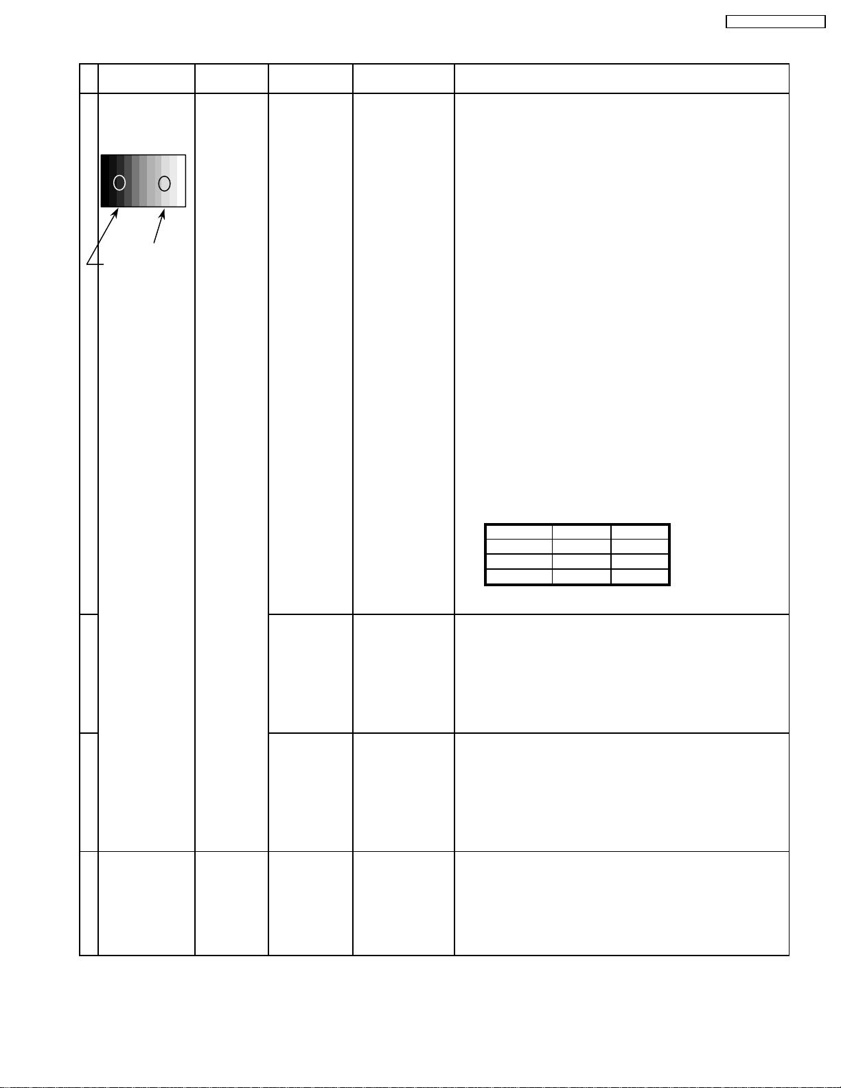
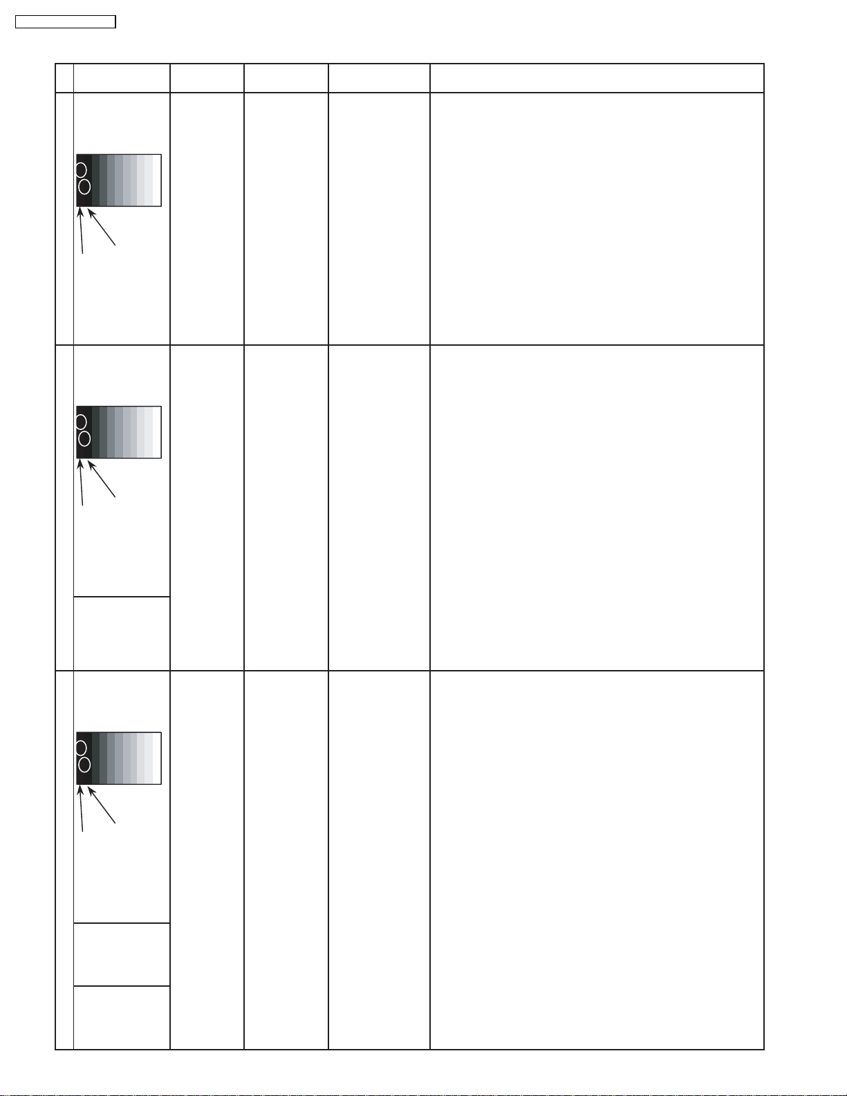
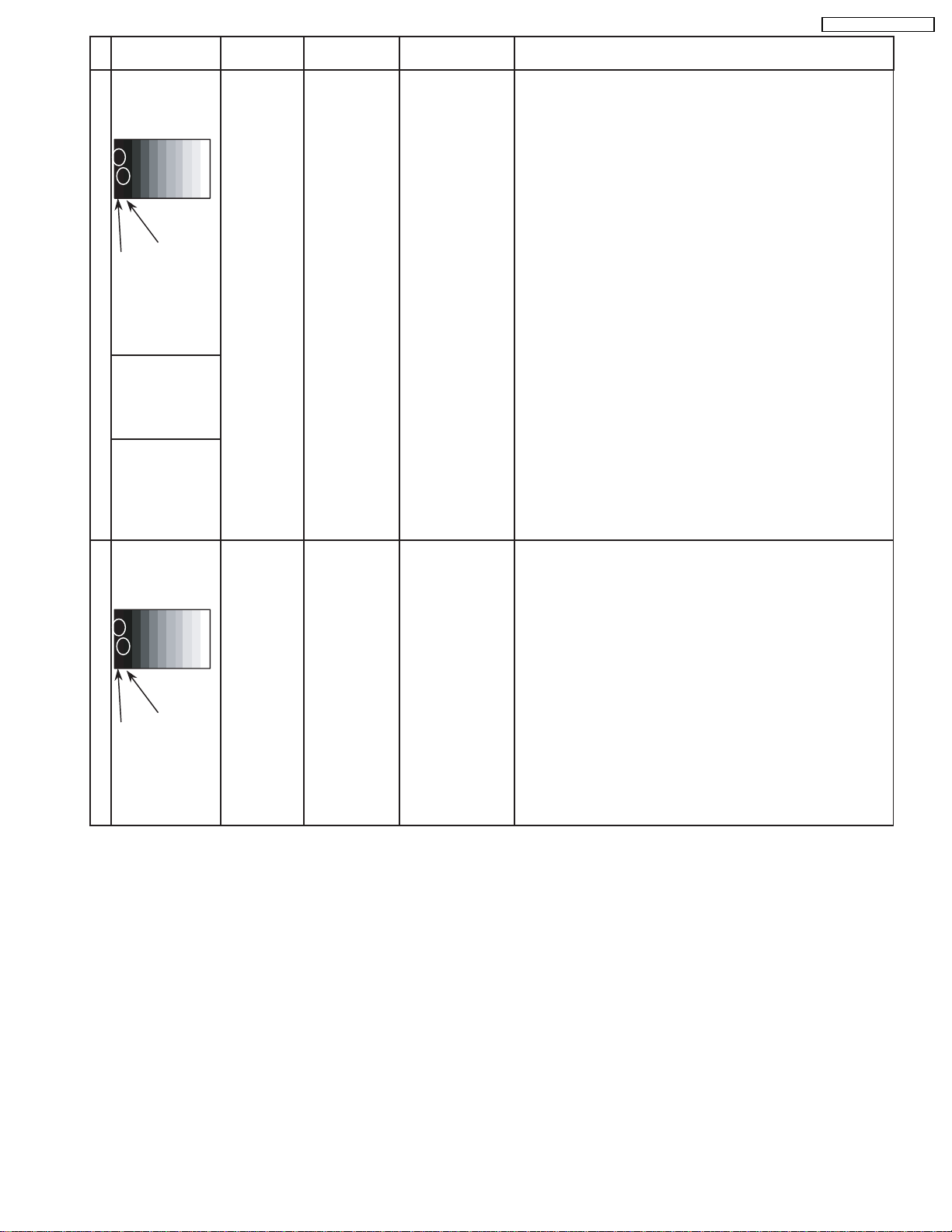
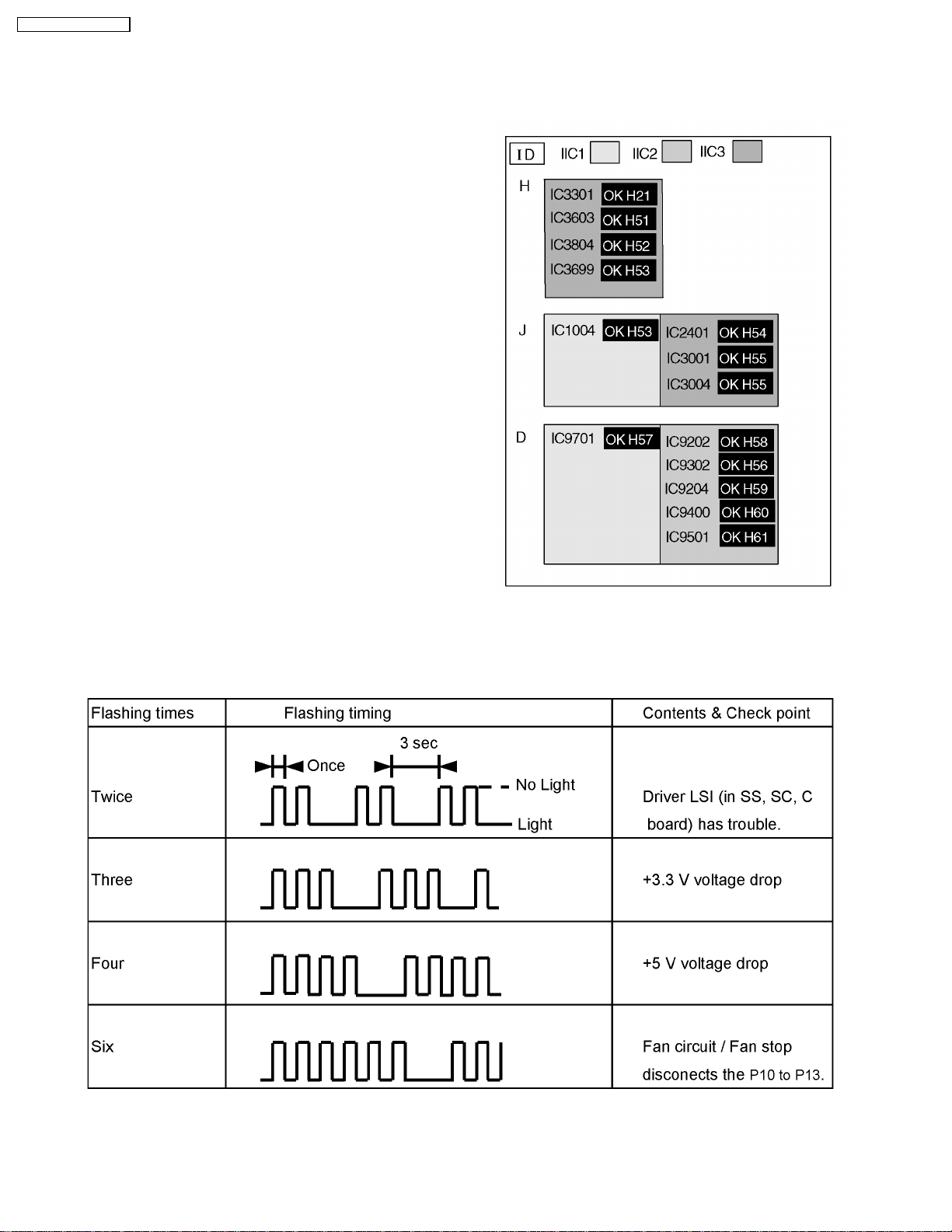
9.1.1. Display Indication
1. Self-check is used to automatically check the bus line
controlled circuit of the Plasma display.
2. To get into the Self-check mode press the volume down
button on the customer controls at the front of the set, at the
same time pressing the OFF-TIMER button on the remote
control, and the screen will show :-
If the CCU ports have been checked and found to be incorrect
Or not located then " - - " will appear in place of " OK "
Note:
In case of disconnected of HZ “IC3699 - -” is displayed.
9.1.2. Power LED Flashing timing chart
When an abnormality has occurred the unit, the protection circuit operates and cuts the power supply. At this time, the defective
part can be identified by the number of flashes of the Power LED at the front of the unit.
Above Fan function is operated during the fan is set.
26
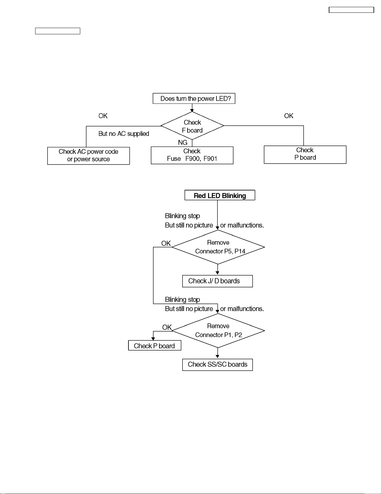
9.2. No Power (US model)
First check point
There are following 3 states of No Power indication by power LED.
1. No lit
2. Green is lit then turns red blinking a few seconds later.
3. Only red is lit.
1. No lit
2. Red LED Blinking
When one or some of supply voltages from power supply circuit are declined red LED will be blinking as power
TH-37PW4 / TH-37PWD4
27
TH-37PW4 / TH-37PWD4
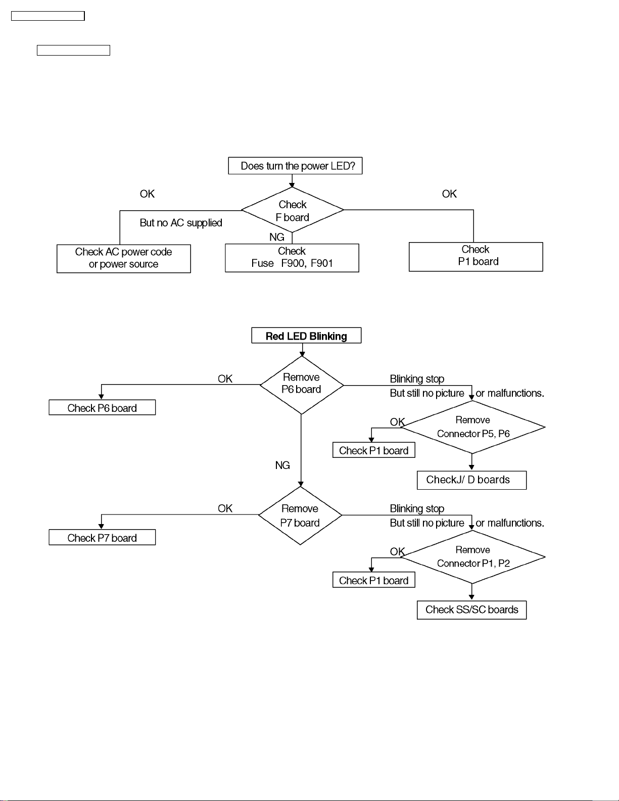
9.3. No Power (Except US)
First check point
There are following 3 states of No Power indication by power LED.
1. No lit
2. Green is lit then turns red blinking a few seconds later.
3. Only red is lit.
1. No lit
2. Red LED Blinking
When one or some of supply voltages from power supply circuit are declined red LED will be blinking as power
28
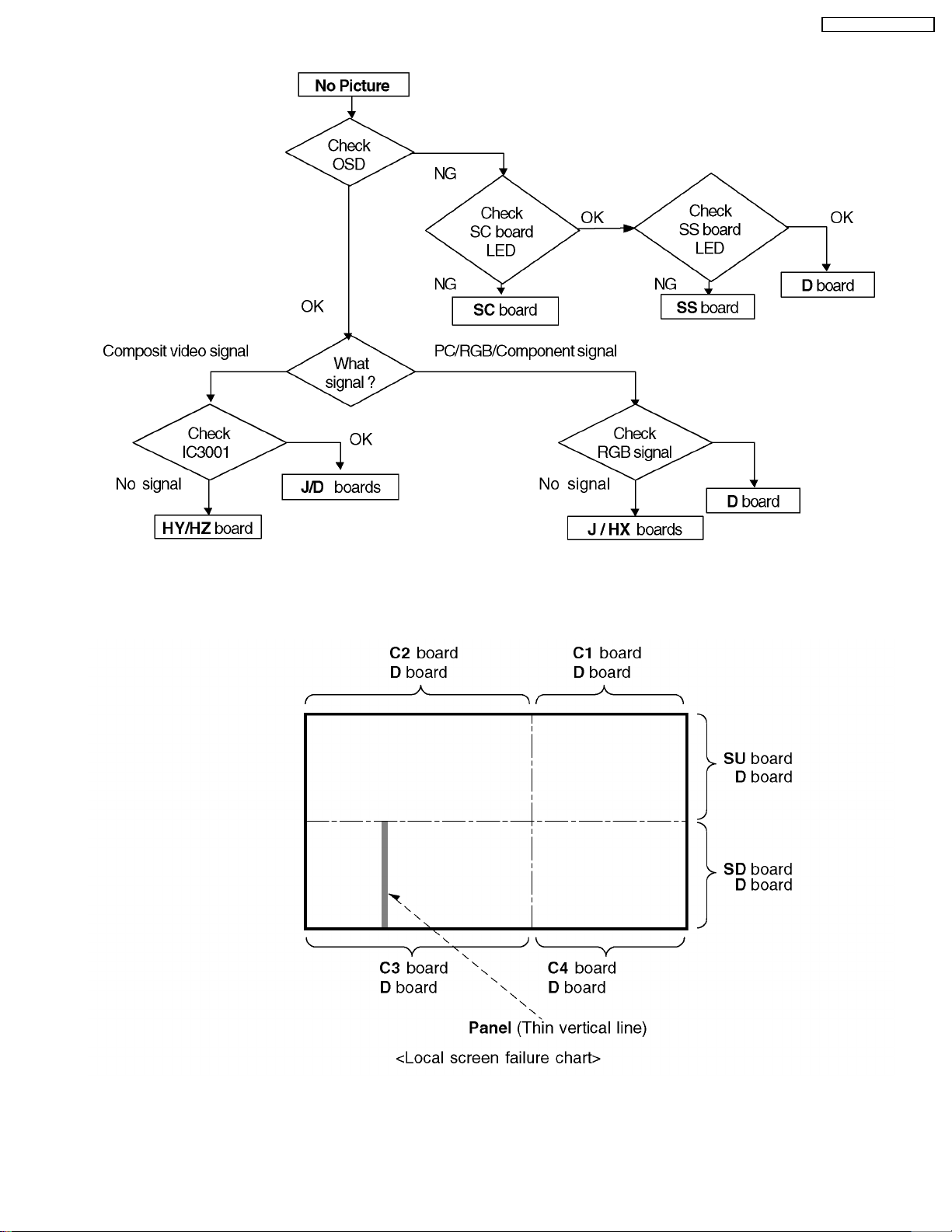
9.4. No Picture
TH-37PW4 / TH-37PWD4
9.5. Local screen failure
Plasma display may have local area failure on the screen. Fig - 1 is the possible defect P.C.B. for each local area.
Fig - 1
29

TH-37PW4 / TH-37PWD4
9.6. D-Board
9.6.1. OUTLINE
D board is consists of Analogue and Digital signal process, Discharge control and Micro control block.
D-board is operated by supply voltages of 3.3V, 5V, 13,5V and Standby 5V , RGB analogue (0.7Vp-p) and Sync. Signal.
D-board output parallel data video signal with control signal for the data driver circuit, Discharge control signal for Scan and Sustain
drive circuits and Micro control signals.
9.6.2. MAIN IC OPERATION
IC9007 ~ 9009 A/D Converter
RGB analogue signals are converted to 8 bits digital signal.
IC9204 FORMAT CONVERTER (LSI33)
Number of Horizontal line of input signals are converted to 480 lines.
This IC uses two clock lines, one is 15M 55MHz for input signal (ICK) and other one is 25M to 40MHz for out put signal. (OCK)
IC9400 PLASMA AI (LSI27)
At first input 8 bit signal data is memorized into two field memory (IC9402, IC9403), Plasma AI analyze APL level and
distribution of dark and bright components.
Plasma AI re-arrange 8 bit signal data to 12 bit signal data.
This IC also insert OSD (On-Screen Display signal) from Micro.
IC9501 SUB FIELD PROCESSOR
R,G and B 12 bit signal data is layout to fit with each electrodes of panel.
One field signal data is separated to upper 240 lines and lower 240 lines.
Both upper and lower signals are again separated odd and even number line and output.
9.6.3. DIAGNOSTIC
(1) General
Depend on the phenomenon possible defective section from Signal processing, Discharge control or Micro control section on
D-board can be diagnosed as follows.
1. Signal Processing section
a. No picture but panel has discharge.
b. Missing R, G or B signal
c. Dark Picture.
d. No OSD signal.
e. Vertical band noise appeared.
f. No picture or distortion on 1/4 area on the screen.
2. Micro control section
a. Does not turn on power.
b. No panel discharge.
3. Discharge control section
a. No discharge but Micro control is operated.
b. Dark picture
30
 Loading...