

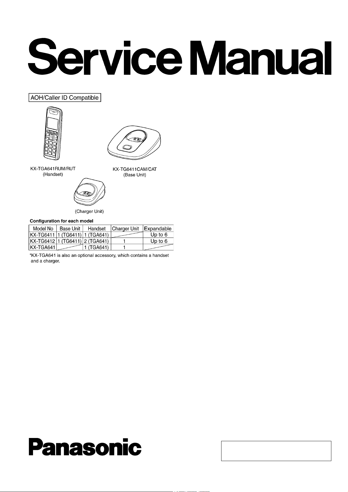
PANASONIC TX-TG6411, TX-TG12, TGA641 Service Manual
ORDER NO. KM40902817CE
Telephone Equipment
Model No.
KX-TG6411CAM
KX-TG6411CAT
KX-TG6412CAM
KX-TG6412CAT
KX-TGA641RUM
KX-TGA641RUT
Digital Cordless Phone
M:Metallic Grey Version
T:Titanium Black Version
(for Kazakhstan)
(for Tajikistan)
(for Uzbekistan)
(for Turkmenistan)
(for Kyrgyzstan)
© Panasonic Communications Co., Ltd. 2009.
Unauthorized copying and distribution is a violation of law.
KX-TG6411CAM/KX-TG6411CAT/KX-TG6412CAM/KX-TG6412CAT/KX-TGA641RUM/KX-TGA641RUT
2

TABLE OF CONTENTS
PAG E PAG E
1 Safety Precautions ----------------------------------------------- 4
1.1. For Service Technicians --------------------------------- 4
2 Warning-------------------------------------------------------------- 4
2.1. Battery Caution--------------------------------------------- 4
2.2. About Lead Free Solder (Pbf: Pb free)--------------- 4
2.3. Discarding of P.C. Board--------------------------------- 5
3 Specifications ----------------------------------------------------- 6
4 Technical Descriptions ----------------------------------------- 7
4.1. Block Diagram (Base Unit) ------------------------------ 7
4.2. Circuit Operation (Base Unit) --------------------------- 8
4.3. Block Diagram (Handset)-------------------------------11
4.4. Circuit Operation (Handset)----------------------------12
4.5. Circuit Operation (Charger Unit) ----------------------13
4.6. Signal Route -----------------------------------------------14
5 Location of Controls and Components ------------------15
5.1. Controls -----------------------------------------------------15
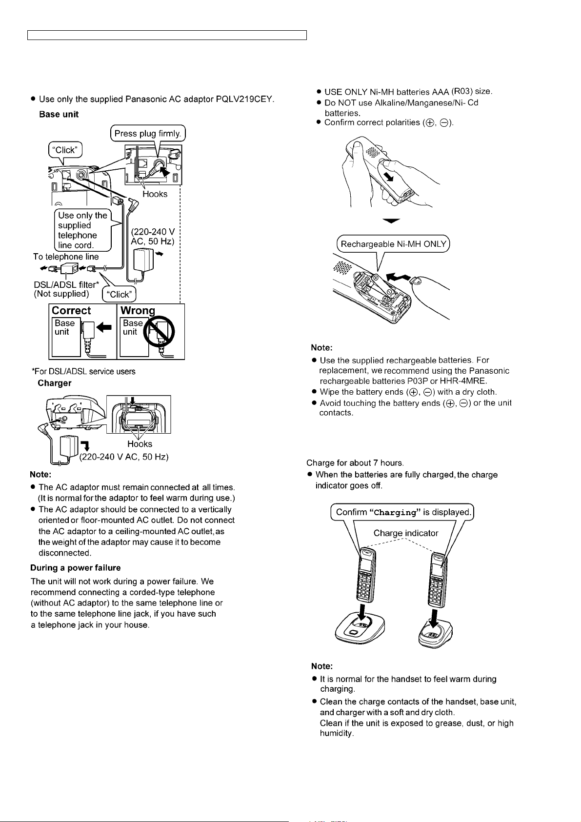
6 Installation Instructions ---------------------------------------16
6.1. Connections------------------------------------------------16
6.2. Battery-------------------------------------------------------16
7 Operating Instructions-----------------------------------------18
7.1. Programmable Settings ---------------------------------18
7.2. Registering a Handset to a Base Unit ---------------20
7.3. Copying Phonebook Entries ---------------------------20
7.4. Dialling Mode ----------------------------------------------21
7.5. Error Messages -------------------------------------------21
7.6. Troubleshooting-------------------------------------------22
7.7. For Service Hint-------------------------------------------26
8 Service Mode -----------------------------------------------------27
8.1. Engineering Mode ----------------------------------------27
8.2. Copying Phonebook Items when Repairing -------31
8.3. How to Clear User Setting------------------------------33
9 Troubleshooting Guide ----------------------------------------34
9.1. Troubleshooting Flowchart -----------------------------34
9.2. Troubleshooting by Symptom (Base Unit and
Charger Unit) ----------------------------------------------46
9.3. Troubleshooting by Symptom (Handset) -----------50
10 Disassembly and Assembly Instructions ---------------54
10.1. Disassembly Instructions -------------------------------54
10.2. How to Replace the Handset LCD -------------------57
11 Measurements and Adjustments---------------------------58
11.1. Equipment Required -------------------------------------58
11.2. The Setting Method of JIG (Base Unit) -------------58
11.3. Adjustment Standard (Base Unit)---------------------60
11.4. Adjustment Standard (Charger Unit)-----------------61
11.5. The Setting Method of JIG (Handset) ---------------62
11.6. Adjustment Standard (Handset) ----------------------64
11.7. Things to Do after Replacing IC or X'tal ------------65
11.8. RF Specification-------------------------------------------67
11.9. How to Check the Handset Speaker or
Receiver ----------------------------------------------------68
11.10. Frequency Table (MHz) ---------------------------------68
12 Miscellaneous ----------------------------------------------------69
12.1. CPU Data (Base Unit) -----------------------------------69
12.2. CPU Data (Handset)-------------------------------------71
12.3. How to Replace the Flat Package IC ----------------73
12.4. How to Replace the LLP (Leadless Leadframe
Package) IC------------------------------------------------75
KX-TG6411CAM/KX-TG6411CAT/KX-TG6412CAM/KX-TG6412CAT/KX-TGA641RUM/KX-TGA641RUT
12.5. Terminal Guide of the ICs, Transistors and
Diodes ------------------------------------------------------ 77
13 Schematic Diagram -------------------------------------------- 79
13.1. For Schematic Diagram -------------------------------- 79
13.2. Schematic Diagram (Base Unit)---------------------- 80
13.3. Schematic Diagram (Handset)------------------------ 82
13.4. Schematic Diagram (Charger Unit)------------------ 84
14 Printed Circuit Board ------------------------------------------ 85
14.1. Circuit Board (Base Unit_Main) ---------------------- 85
14.2. Circuit Board (Handset) -------------------------------- 87
14.3. Circuit Board (Charger Unit)--------------------------- 89
15 Exploded View and Replacement Parts List ----------- 90
15.1. Cabinet and Electrical Parts (Base Unit) ----------- 90
15.2. Cabinet and Electrical Parts (Handset)------------- 91
15.3. Cabinet and Electrical Parts (Charger Unit) ------- 92
15.4. Accessories and Packing Materials ----------------- 93
15.5. Replacement Part List ---------------------------------- 96
3
KX-TG6411CAM/KX-TG6411CAT/KX-TG6412CAM/KX-TG6412CAT/KX-TGA641RUM/KX-TGA641RUT
1 Safety Precautions
1.1. For Service Technicians
• Repair service shall be provided in accordance with repair technology information such as service manual so as to prevent fires, injury or electric shock, which can be caused by improper repair work.
1. When repair services are provided, neither the products nor their parts or members shall be remodeled.
2. If a lead wire assembly is supplied as a repair part, the lead wire assembly shall be replaced.
3. FASTON terminals shall be plugged straight in and unplugged straight out.
• ICs and LSIs are vulnerable to static electricity.
When repairing, the following precautions will help prevent recurring malfunctions.
1. Cover plastic parts boxes with aluminum foil.
2. Ground the soldering irons.
3. Use a conductive mat on worktable.
4. Do not grasp IC or LSI pins with bare fingers.
2Warning
2.1. Battery Caution
1. Danger of explosion if battery is incorrectly replaced.
2. Replace only with the same or equivalent type recommended by the manufacturer.
3. Dispose of used batteries according to the manufacture’s Instructions.
2.2. About Lead Free Solder (Pbf: Pb free)
Note:
In the information below, Pb, the symbol for lead in the periodic table of elements, will refer to standard solder or solder that contains lead.
We will use PbF solder when discussing the lead free solder used in our manufacturing process which is made from Tin (Sn),
Silver (Ag), and Copper (Cu).
This model, and others like it, manufactured using lead free solder will have PbF stamped on the PCB. For service and repair
work we suggest using the same type of solder.
Caution
• PbF solder has a melting point that is 50 °F ~ 70 °F (30 °C ~ 40 °C) higher than Pb solder. Please use a soldering iron with
temperature control and adjust it to 700 °F ± 20 °F (370 °C ± 10 °C).
• Exercise care while using higher temperature soldering irons.:
Do not heat the PCB for too long time in order to prevent solder splash or damage to the PCB.
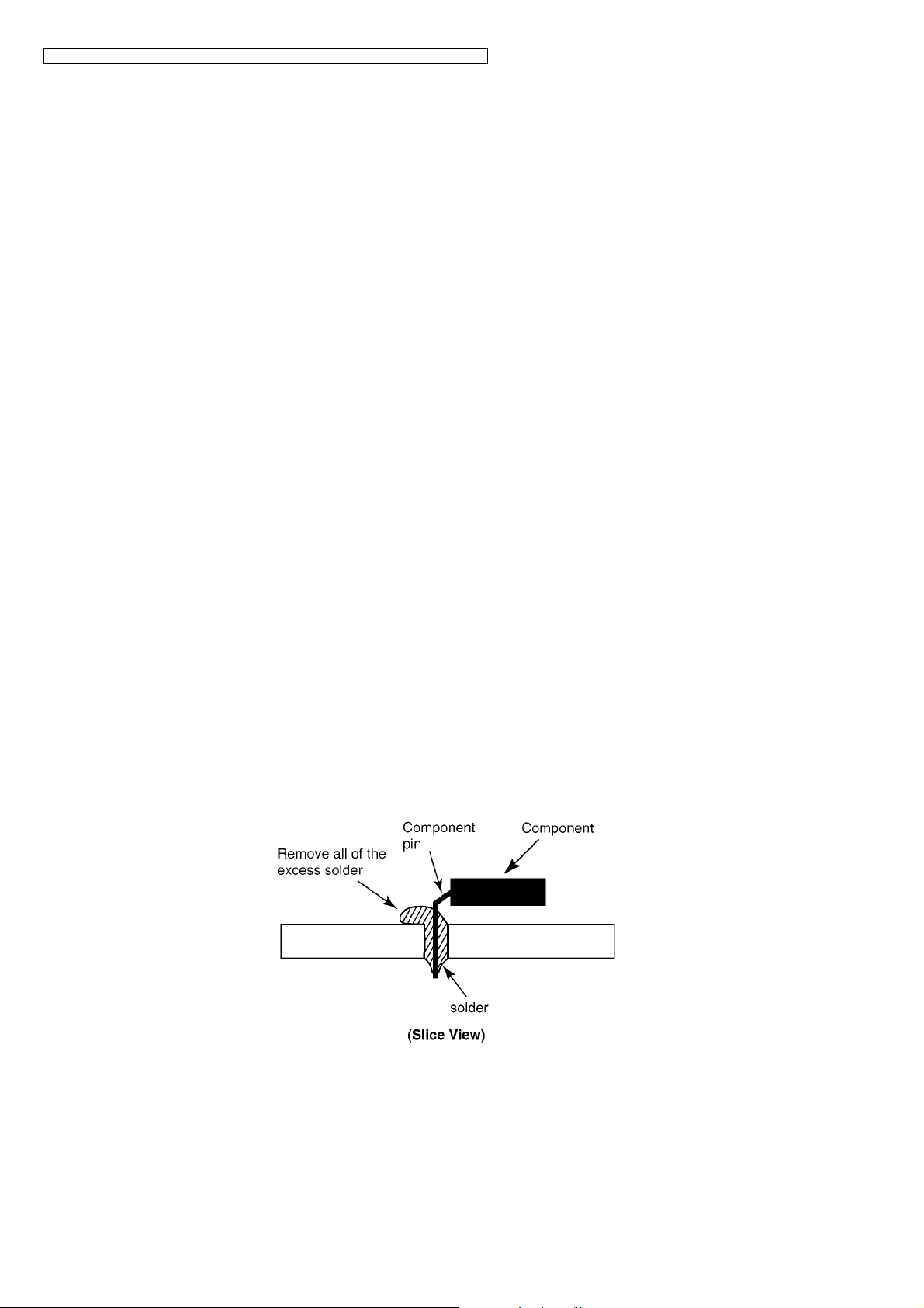
• PbF solder will tend to splash if it is heated much higher than its melting point, approximately 1100 °F (600 °C).
• When applying PbF solder to double layered boards, please check the component side for excess which may flow onto the
opposite side (See the figure below).
4
KX-TG6411CAM/KX-TG6411CAT/KX-TG6412CAM/KX-TG6412CAT/KX-TGA641RUM/KX-TGA641RUT
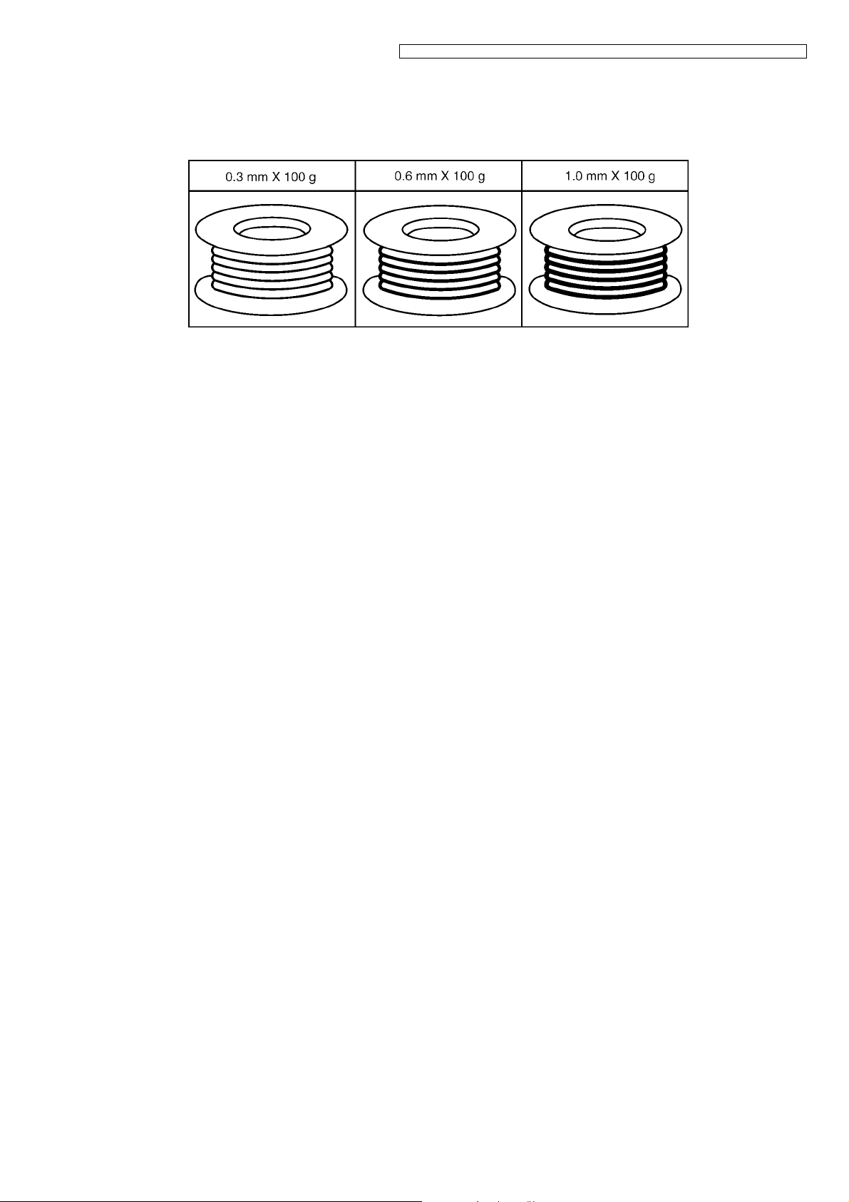
2.2.1. Suggested PbF Solder
There are several types of PbF solder available commercially. While this product is manufactured using Tin, Silver, and Copper
(Sn+Ag+Cu), you can also use Tin and Copper (Sn+Cu) or Tin, Zinc, and Bismuth (Sn+Zn+Bi). Please check the manufacturer’s
specific instructions for the melting points of their products and any precautions for using their product with other materials.
The following lead free (PbF) solder wire sizes are recommended for service of this product: 0.3 mm, 0.6 mm and 1.0 mm.
2.3. Discarding of P.C. Board
When discarding P. C. Board, delete all personal information such as telephone directory and caller list or scrap P. C. Board.
5
KX-TG6411CAM/KX-TG6411CAT/KX-TG6412CAM/KX-TG6412CAT/KX-TGA641RUM/KX-TGA641RUT
3 Specifications
Note:
• Design and specifications are subject to change without notice.
Note for Service:
• Operation range: Up to 300 m outdoors, Up to 50 m indoors, depending on the condition.
• Analog telephone connection: Telephone Line
6
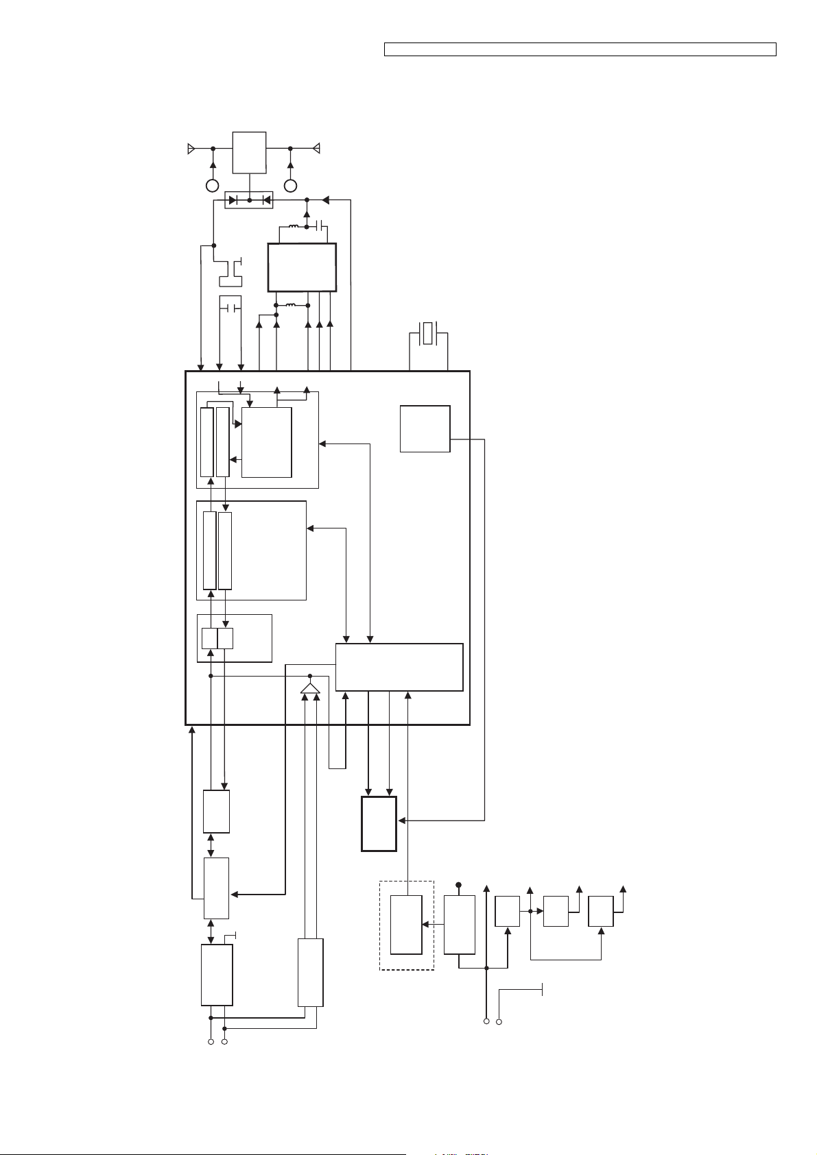
4 Technical Descriptions
D3
4.1. Block Diagram (Base Unit)
KX-TG6411CAM/KX-TG6411CAT/KX-TG6412CAM/KX-TG6412CAT/KX-TGA641RUM/KX-TGA641RUT
ANT1
on
RX
5
ANT1
ANT1
6
D801
-PADRV
p
n
DD
RX
V
RX
3
2
Burst Decoding
Burst Encoding
ANT2
ANT2
9
4
p
TX
77
75
RF
PLL
MOD/DEMOD
72
RF PA
n
TX
ANT2
8
IC801
7
6
3
on
P
PSEL
787374
BMC
on
TX
80
XTAL
BBIC
X1
IC7
9
Charge
MHz
10.368
Pump
10
43
KX-TG6411/6412 BLOCK DIAGRAM (BASE UNIT)
ADPCM
Speech Encoding
Speech Decoding
Front
Analog
End
25
18
A/D
D/A
16
Audio
Off-Hook Line Voltage
Q4,Q5
Hook Switch
DSP
Codec Filter
23
20
211924
HOOK
CPU
57
BELL
SCL
(Optional)
44
58
SDA
IC401
EEPROM
Charge
Detector
2.5V
CHARGE
CONTACT
Limit
Resistor
VUNREG
IC1
Reg.
3.0V
3.0 V
Q9
2.4V
Reg.
2.4 V
Q8
1.8V
1.8 V
Reg.
Bridge
L1
To TEL_LINE
Rect D3
L2
Interface
Bell/Caller ID
L2
L1
To AC Adaptor
7

KX-TG6411CAM/KX-TG6411CAT/KX-TG6412CAM/KX-TG6412CAT/KX-TGA641RUM/KX-TGA641RUT
4.2. Circuit Operation (Base Unit)
4.2.1. Outline
Base Unit consists of the following ICs as shown in Block Diagram (Base Unit) (P.7).
• DECT BBIC (Base Band IC): IC7
- Handling all the audio, signal and data processing needed in a DECT base unit
- Controlling the DECT specific physical layer and radio section (Burst Module Controller section)
- ADPCM code filter for speech encoding and speech decoding (DSP section)
- Echo-cancellation and Echo-suppression (DSP section)
- Any tones (tone, sidetone, ringing tone, etc.) generation (DSP section)
- DTMF receiver (DSP section)
- Clock Generation for RF Module
- ADC, DAC, timer, and power control circuitry
- PLL Oscillator
- Detector
- Compress/Expander
- First Mixer
- All interfaces (ex: RF Power Amp, EEPROM, LED, Analog Front End, etc.)
• RF Power Amp.: IC801
- Amplifier for transmission and reception
• EEPROM: IC401
- Temporary operating parameters (for RF, etc.)
• Additionally,
- Power Supply Circuit (+3.0 V, +2.4 V, +1.8 V output)
- Crystal Circuit (10.368 MHz)
- Charge Circuit
- Telephone Line Interface Circuit
8
KX-TG6411CAM/KX-TG6411CAT/KX-TG6412CAM/KX-TG6412CAT/KX-TGA641RUM/KX-TGA641RUT
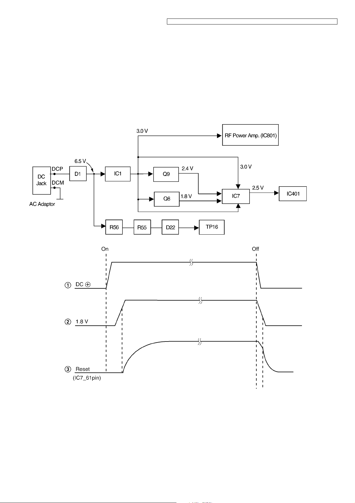
4.2.2. Power Supply Circuit
The power is supplied to the DECT BBIC, RF Module, EEPROM and Charge Contact from AC Adaptor (+6.5 V) as shown in
Fig.101. The power supply is as follows;
• DECT BBIC (IC7):
DC Jack (+6.5 V) →D1→ IC1 → IC7
DC Jack (+6.5 V) →D1→ IC1 → Q9 → IC7
DC Jack (+6.5 V) →D1→ IC1 → Q8 → IC7
• RF Power Amp. (IC801):
DC Jack (+6.5 V) →D1→ IC1 → IC801 (Power AMP)
• EEPROM (IC401):
DC Jack (+6.5 V) →D1→ IC1 → IC7→ IC401
• Charge Contact (TP16):
DC Jack (+6.5 V) →D1→ R56 → R55 → D22→ TP16
<Fig.101>
9

KX-TG6411CAM/KX-TG6411CAT/KX-TG6412CAM/KX-TG6412CAT/KX-TGA641RUM/KX-TGA641RUT
4.2.3. Telephone Line Interface
<Function>
• Bell signal detection
• Clip signal detection
• ON/OFF hook circuit
Bell & Clip (: Calling Line Identification Presentation: Caller ID) signal detection:
In the standby mode, Q3 is open to cut the DC loop current and decrease the ring load.
When ring voltage appears at the L1T (A) and L1R (B) leads (when the telephone rings), the AC ring voltage is transferred as
follows;
•B → L2 → C4 → R6 → R33 → IC7 Pin 21 (CID INp)
•A → L1 → C3 → R4 → R35 → IC7 Pin 20 (CID INn)
ON/OFF hook circuit:
In the standby mode, Q3 is open, and connected as to cut the DC loop current and to cut the voice signal. The unit is consequently in an on-hook condition.
When IC7 detects a ring signal or press the TALK Key onto the handset, Q4 turns on and then Q3 turns on, thus providing an
off-hook condition (DC current flows through the circuit) and the following signal flow makes the loop current.
•B → L2 →D3 → Q3 → Q5 → R21 → R22 → D3 → L1 →A [OFF HOOK]
4.2.4. Transmitter/Receiver
• Audio Circuits and DTMF tone signal circuits.
Base Unit and Handset mainly consist of RF Module and DECT BBIC.
Base Unit and Handset transmit/receive voice signal and data signal through the antenna on carrier frequency.
Signal Path:
*Refer to Signal Route (P.14).
4.2.4.1. Transmitter Block
The voice signal input from the TEL LINE interface goes to RF Power Amp. (IC801) through DECT BBIC (IC7) as shown in
Block Diagram (Base Unit) (P.7)
The voice signal passes through the analog part of IC7 where it is amplified and converted to a digital audio stream signal. The
burst switch controller processes this stream performing encryption and scrambling, adding the various other fields to produce
the GAP (Generic Access Profile) standard DECT frame, assigning to a time slot and channel etc.
In IC7, the carrier frequency is changing, and frequency modulated RF signal is generated.In IC801,RF signal is amplified, and
radiated from antenna. Handset detects the voice signal or data signal in the circuit same as the following explanation of
Receiver Block.
4.2.4.2. Receiver Block
The signal of 1900 MHz band (1881.792 MHz ~ 1897.344 MHz) which is input from antenna is input to IC7 as shown in Block
Diagram (Base Unit) (P.7).
In IC7, the signal of 1900 MHz band is downconverted to 864 kHz signal and demodulated, as GAP (Generic Access Profile)
standard DECT frames. It passes through the decoding section burst switch controller where it separates out the frame information and performs de-encryption and de-scrambling as required. It then goes to the DSP section where it is turned back into ana-
log audio. This is amplified by the analog front end, and goes to the TEL LINE Interface.
4.2.4.3. Pulse Dialling
During pulse dialing the hookswitch (Q3, Q4) is used to generate the pulses using the HOOK control signal, which is set high
during pulses. To force the line impedance low during the “pause” intervals between dial pulses, the PULSE_DIAL signal turns
on Q2.
10
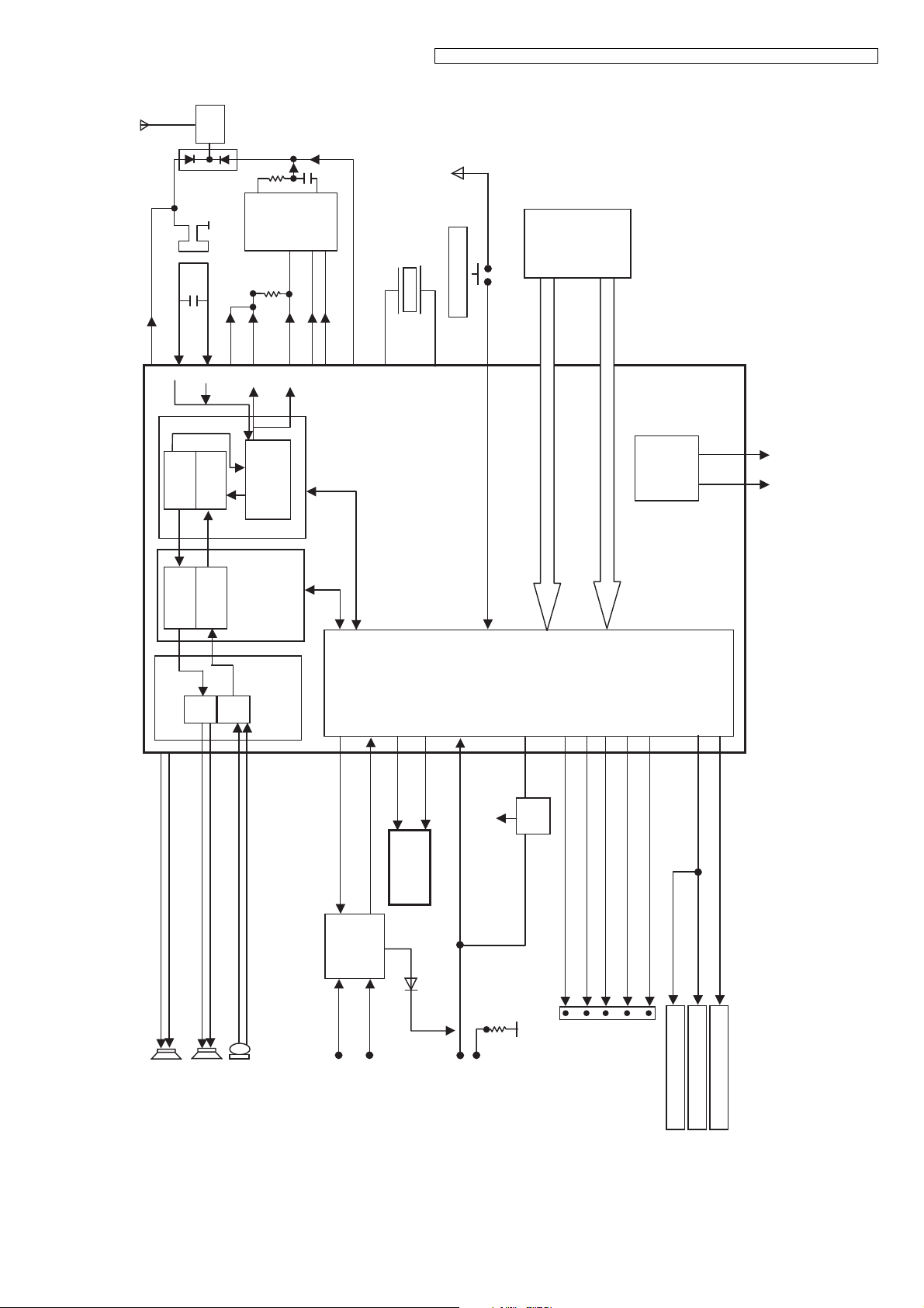
4.3. Block Diagram (Handset)
Q4, Q9, R7
ANT1
ANT1
KX-TG6411CAM/KX-TG6411CAT/KX-TG6412CAM/KX-TG6412CAT/KX-TGA641RUM/KX-TGA641RUT
RXon
5
RXn
3
Burst
Decoding
Speech
Decoding
DA801
VDD-PADRY
RXp
TXp
2
75
Burst
Encoding
ADPCM
Speech
Encoding
9
RF PA
4
TXn
77
RF
PLL
MOD/DEMOD
Filter
Codec
8
IC801
367
Pon
PSEL
737480
78
BMC
DSP
TXon
X1
XTAL
9
10.368
MHz
10
BATTERY
ON SWITCH
44
KEYPAD
ROWS
COLUMNS
48, 49, 50, 51
22, 23, 24, 25, 26
Pump
Charge
IC1
BBIC
43 42
CP3.0 V CP4.0 V
KX-TGA641 BLOCK DIAGRAM (HANDSET)
33
35
SPEAKER
D/A
A/D
19
15
16
RECEIVER
MIC
Analog
20
End
Front
32
31
CHARGE
CHARGE_CTRL
CHARGE
CIRCUIT
Q4, Q9, R7
CHARGE(+)
CHARGE
CONTACTS
57
58
SCL
SDA
IC3
EEPROM
D7
CHARGE(-)
J1
CPU
36
VBAT
J2
BATTERY
TERMINAL
LDO_CTRL
13
1.8 V
Q2
1.8 V
56
CD
635455
66
CSB
RESET
LCD
SDA
52
SCL
KEY LED
LCD-BACK LIGHT
68
BELL LED
11
KX-TG6411CAM/KX-TG6411CAT/KX-TG6412CAM/KX-TG6412CAT/KX-TGA641RUM/KX-TGA641RUT
4.4. Circuit Operation (Handset)
4.4.1. Outline
Handset consists of the following ICs as shown in Block Diagram (Handset) (P.11).
• DECT BBIC (Base Band IC): IC1
- All data signals (forming/analyzing ACK or CMD signal)
- All interfaces (ex: Key, Detector Circuit, Charge, DC/DC Converter, EEPROM, LCD, RF Power Amp.)
- PLL Oscillator
- Detector
- Compress/Expander
- Reception
• RF Power Amp: IC801
- Amplifier for transmission
• EEPROM: IC3
- Temporary operating parameters (for RF, etc.)
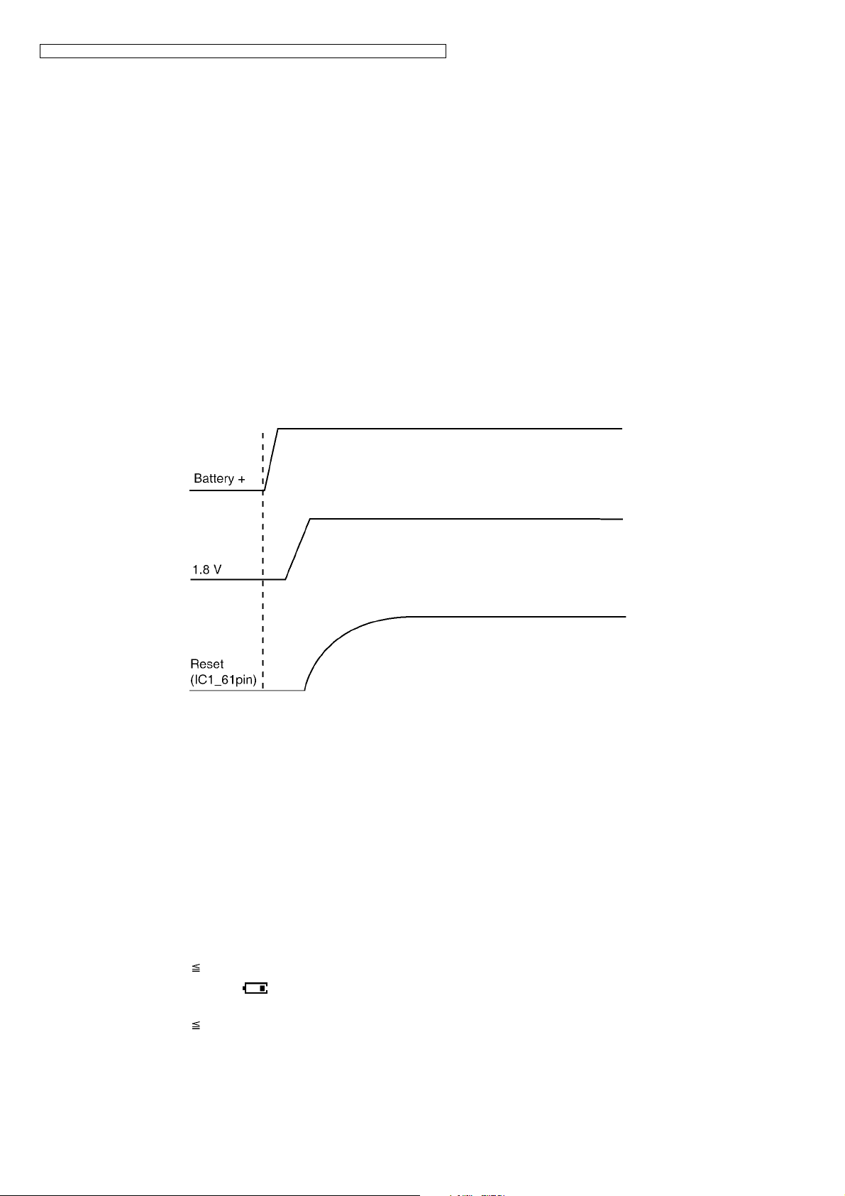
4.4.2. Power Supply Circuit/Reset Circuit
Circuit Operation:
When power on the Handset, the voltage is as follows;
BATTERY(2.2 V ~ 2.6 V: BATT+) → F1 → Q2 (1.8 V), IC1-43pin (2.5V)
The Reset signal generates IC1 (61 pin) and 1.8 V.
4.4.3. Charge Circuit
Circuit Operation:
When charging the handset on the Base Unit, the charge current is as follows;
DC+(6.5 V) → D1 → R56 → R55 → D22 → CHARGE+(Base) → CHARGE+(Handset) → Q4 → D7→ F1 → BATTERY+... Battery...
BATTERY- → R45 → GND → CHARGE-(Handset)→ CHARGE-(Base) → GND → DC-(GND)
In this way, the BBIC on Handset detects the fact that the battery is charged.
The charge current is controlled by switching Q9 of Handset.
Refer to Fig.101 in Power Supply Circuit (P.9).
4.4.4. Battery Low/Power Down Detector
Circuit Operation:
“Battery Low” and “Power Down” are detected by BBIC which check the voltage from battery.
The detected voltage is as follows;
• Battery Low
Battery voltage: V(Batt) 2.25 V ± 50 mV
The BBIC detects this level and " " starts flashing.
• Power Down
Battery voltage: V(Batt) 2.0 V ± 50 mV
The BBIC detects this level and power down.
4.4.5. Speakerphone
The hands-free loudspeaker at SP+ and SP- is used to generate the ring alarm.
12
KX-TG6411CAM/KX-TG6411CAT/KX-TG6412CAM/KX-TG6412CAT/KX-TGA641RUM/KX-TGA641RUT
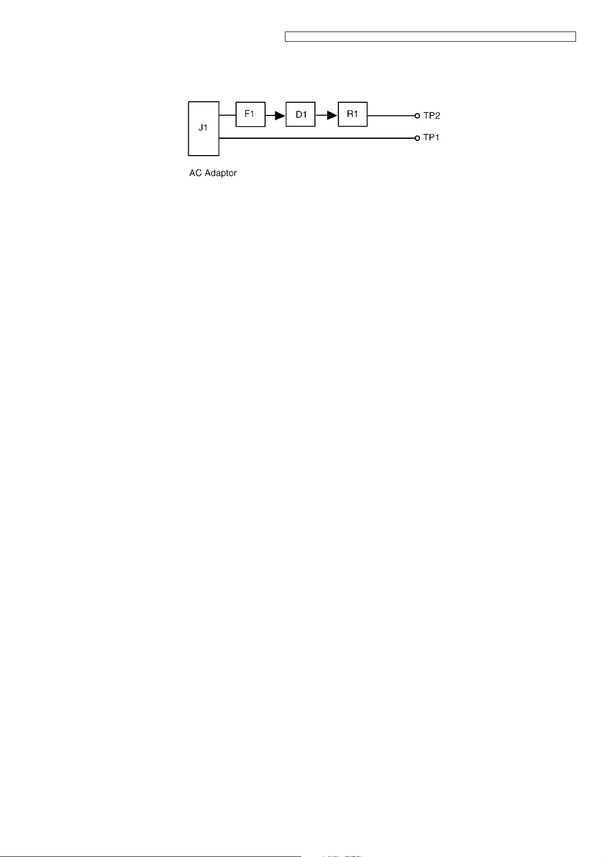
4.5. Circuit Operation (Charger Unit)
4.5.1. Power Supply Circuit
The power supply is as shown.
13
KX-TG6411CAM/KX-TG6411CAT/KX-TG6412CAM/KX-TG6412CAT/KX-TGA641RUM/KX-TGA641RUT
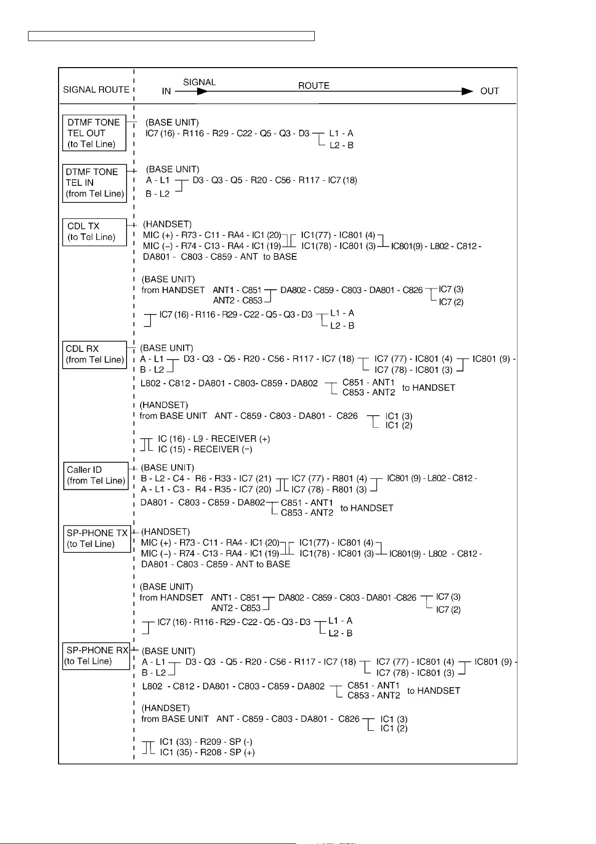
4.6. Signal Route
14
KX-TG6411CAM/KX-TG6411CAT/KX-TG6412CAM/KX-TG6412CAT/KX-TGA641RUM/KX-TGA641RUT
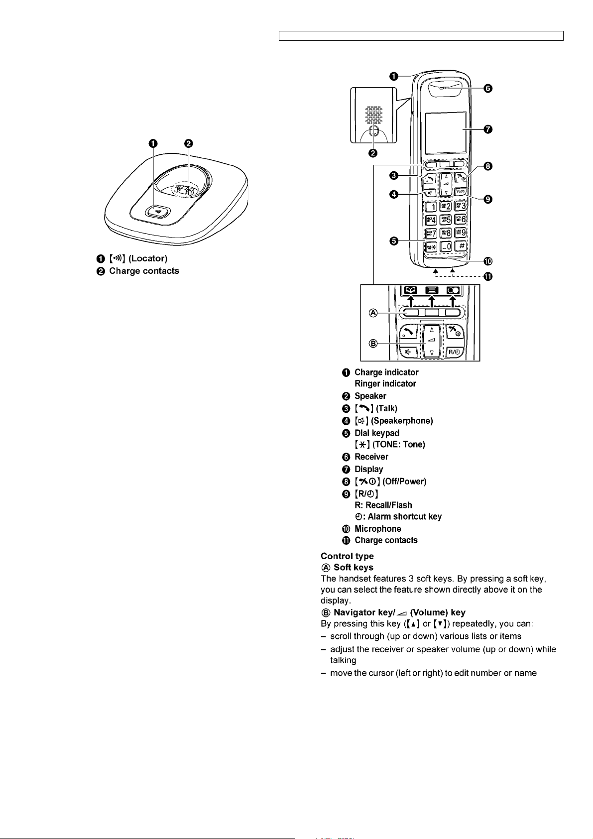
5 Location of Controls and
Components
5.1. Controls
5.1.1. Base Unit
5.1.2. Handset
15
KX-TG6411CAM/KX-TG6411CAT/KX-TG6412CAM/KX-TG6412CAT/KX-TGA641RUM/KX-TGA641RUT
6 Installation Instructions
6.1. Connections
6.2. Battery
6.2.1. Battery Installation
See For Service Hint (P.26)
6.2.2. Battery Charge
16
Note for service:
The battery strength may not be indicated correctly if the
battery is disconnected and connected again, even after it is
fully charged. In that case, by recharging the battery as
mentioned above, you will get a correct indication of the
battery strength.
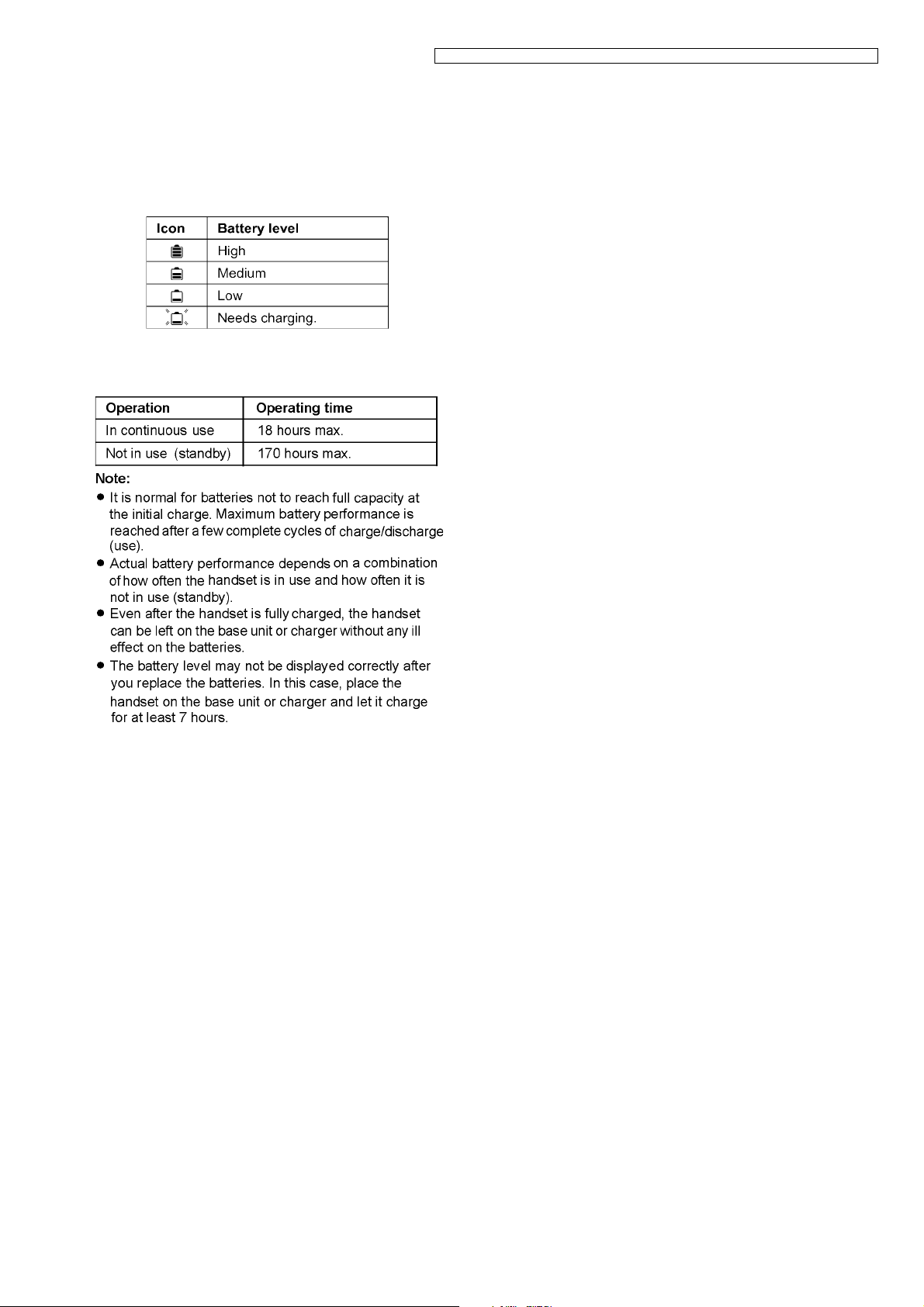
6.2.3. Battery Level
6.2.4. Panasonic Ni-MH Battery
Performance (supplied batteries)
KX-TG6411CAM/KX-TG6411CAT/KX-TG6412CAM/KX-TG6412CAT/KX-TGA641RUM/KX-TGA641RUT
17
KX-TG6411CAM/KX-TG6411CAT/KX-TG6412CAM/KX-TG6412CAT/KX-TGA641RUM/KX-TGA641RUT
7 Operating Instructions
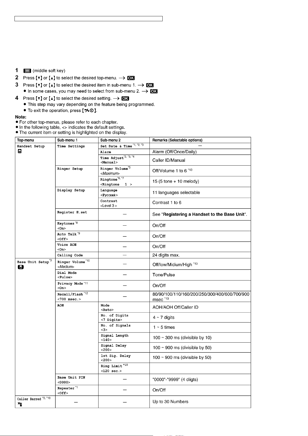
7.1. Programmable Settings
You can customise the unit by programming the following features using the handset.
7.1.1. Programming by scrolling through the display menus
18
KX-TG6411CAM/KX-TG6411CAT/KX-TG6412CAM/KX-TG6412CAT/KX-TGA641RUM/KX-TGA641RUT
*1 The item will not be reset when pressing , , and keys. Refer to How to Clear User Setting (P.33).
*2 The item will not be reset when pressing , , and keys. Refer to How to Clear User Setting (P.33).
Cross Reference:
Registering a Handset to a Base Unit (P.20)
19
KX-TG6411CAM/KX-TG6411CAT/KX-TG6412CAM/KX-TG6412CAT/KX-TGA641RUM/KX-TGA641RUT
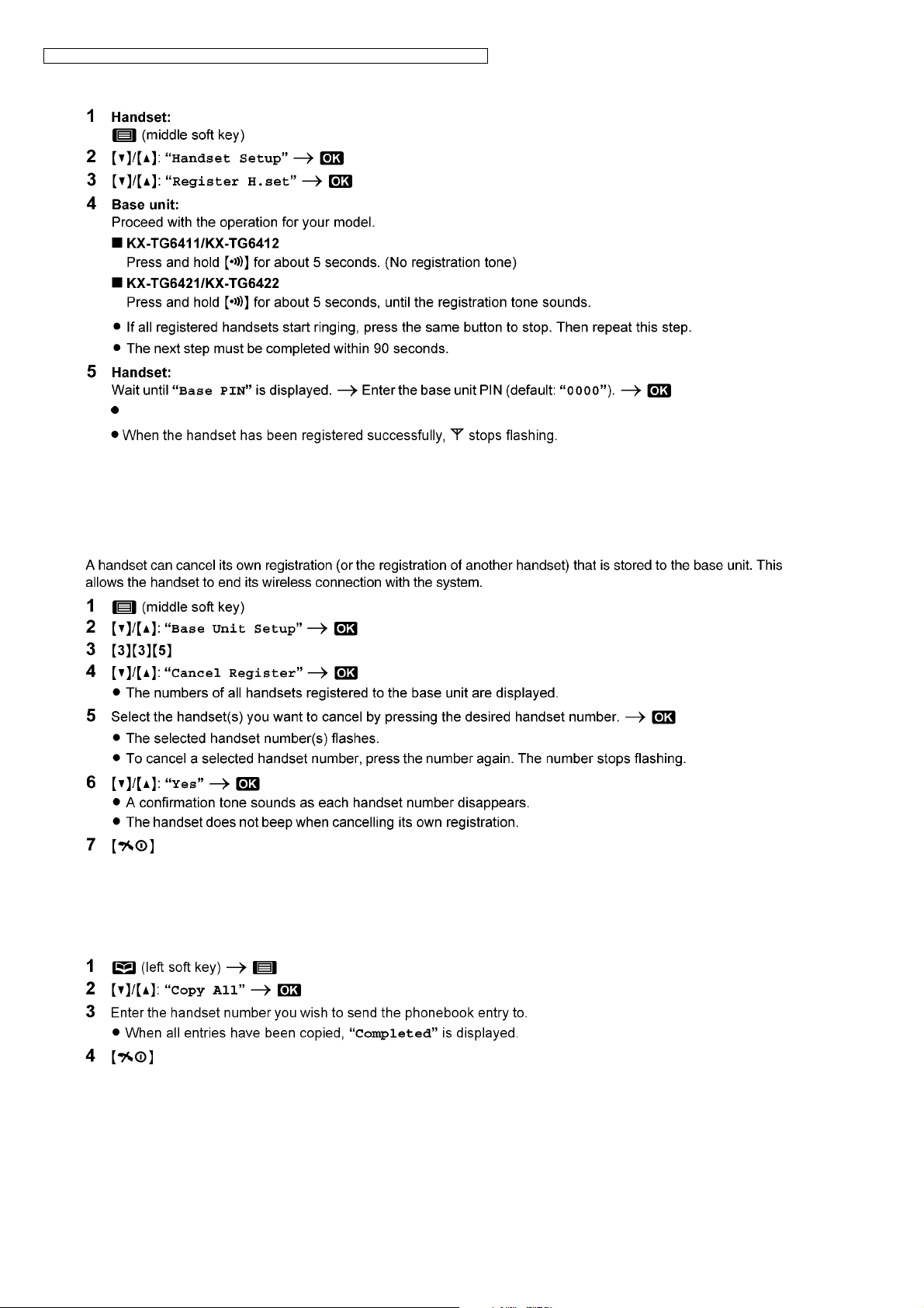
7.2. Registering a Handset to a Base Unit
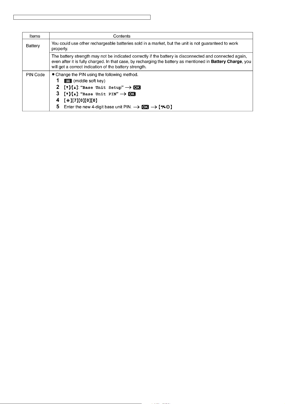
If you forget your PIN, see "For Service Hint ". (P.26)
Note:
• When you purchase an additional handset, refer to the additional handset's installation manual for registration.
Cross Reference:
Troubleshooting (P.22)
7.2.1. Deregistering a Handset
7.3. Copying Phonebook Entries
You can copy phonebook entries to the phonebook of another compatible Panasonic handset.
7.3.1. Copying all entries
20
7.4. Dialling Mode
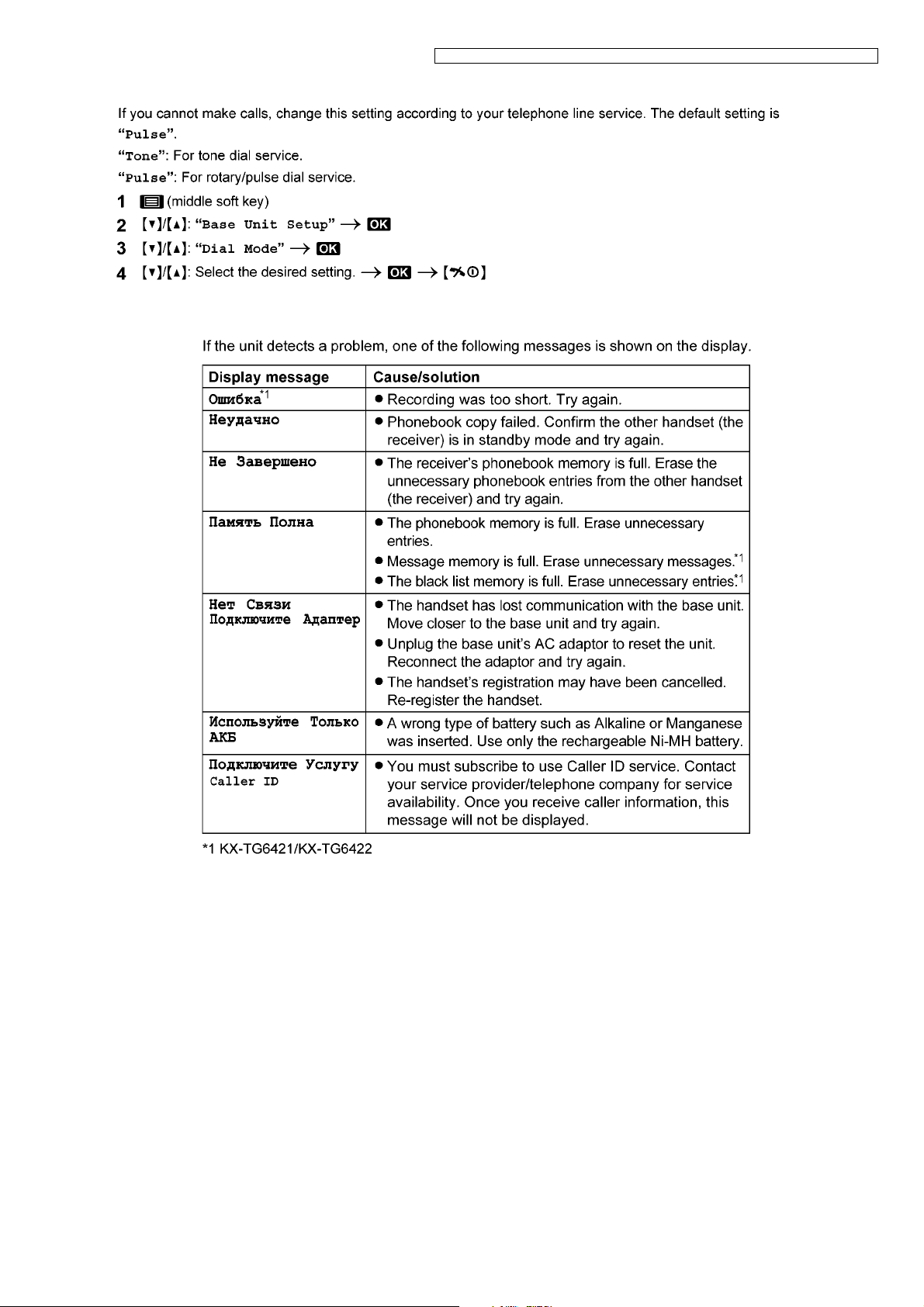
7.5. Error Messages
KX-TG6411CAM/KX-TG6411CAT/KX-TG6412CAM/KX-TG6412CAT/KX-TGA641RUM/KX-TGA641RUT
21
KX-TG6411CAM/KX-TG6411CAT/KX-TG6412CAM/KX-TG6412CAT/KX-TGA641RUM/KX-TGA641RUT
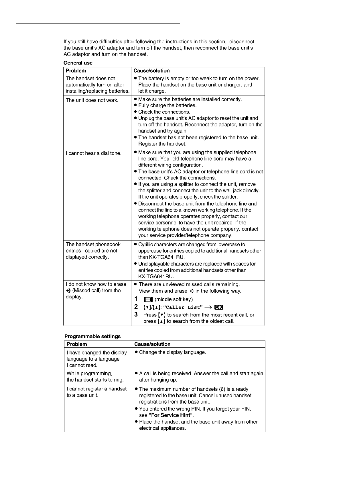
7.6. Troubleshooting
22
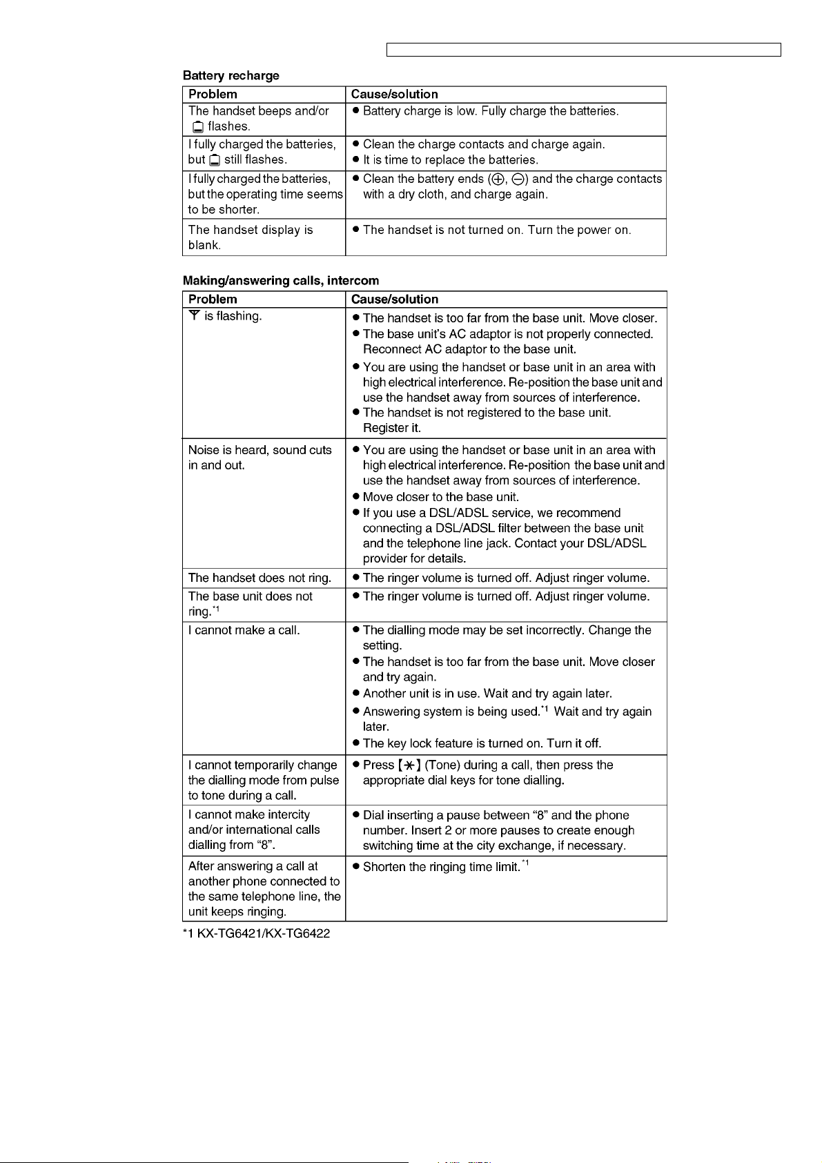
KX-TG6411CAM/KX-TG6411CAT/KX-TG6412CAM/KX-TG6412CAT/KX-TGA641RUM/KX-TGA641RUT
23
KX-TG6411CAM/KX-TG6411CAT/KX-TG6412CAM/KX-TG6412CAT/KX-TGA641RUM/KX-TGA641RUT
24
KX-TG6411CAM/KX-TG6411CAT/KX-TG6412CAM/KX-TG6412CAT/KX-TGA641RUM/KX-TGA641RUT
25
KX-TG6411CAM/KX-TG6411CAT/KX-TG6412CAM/KX-TG6412CAT/KX-TGA641RUM/KX-TGA641RUT
7.7. For Service Hint
Cross Reference:
Battery Charge (P.16)
26
8 Service Mode
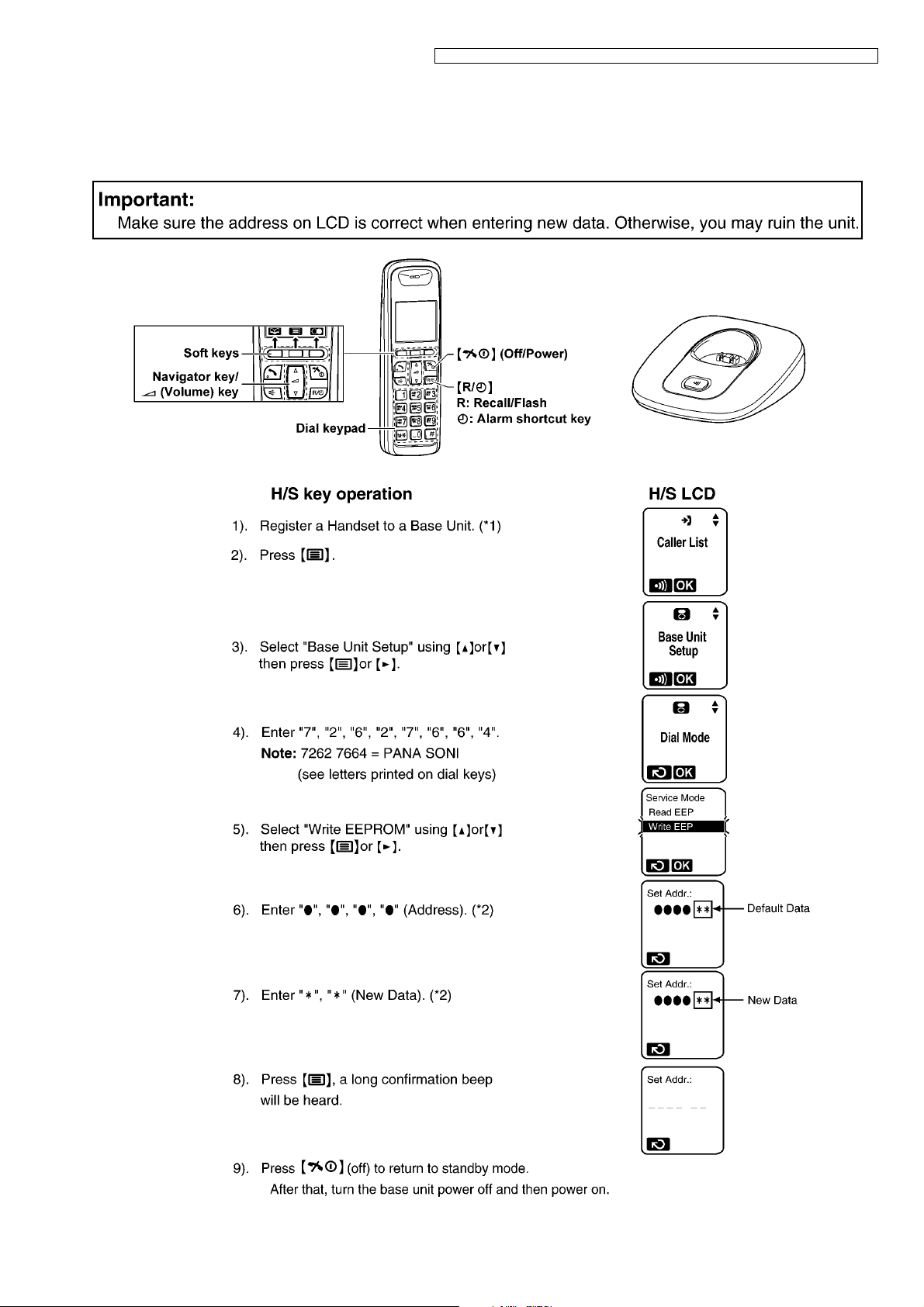
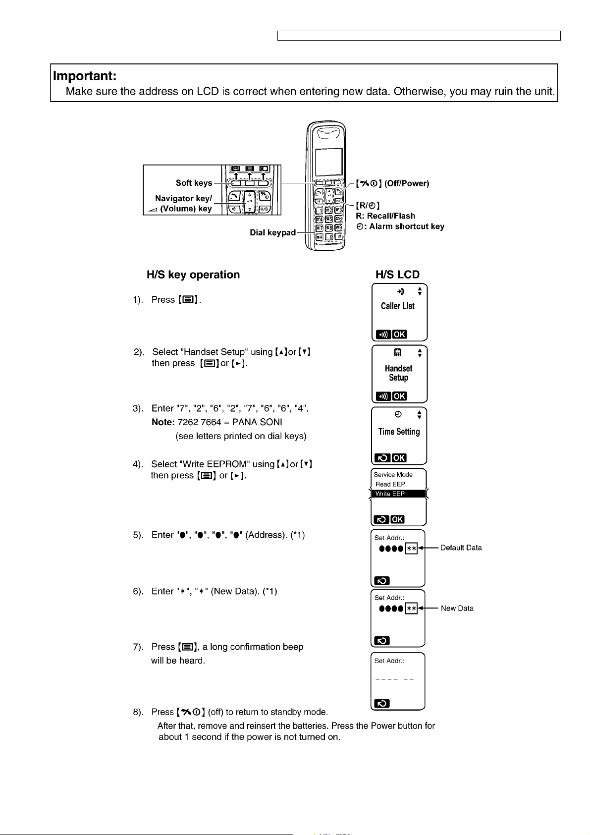
8.1. Engineering Mode
8.1.1. Base Unit
KX-TG6411CAM/KX-TG6411CAT/KX-TG6412CAM/KX-TG6412CAT/KX-TGA641RUM/KX-TGA641RUT
27
KX-TG6411CAM/KX-TG6411CAT/KX-TG6412CAM/KX-TG6412CAT/KX-TGA641RUM/KX-TGA641RUT
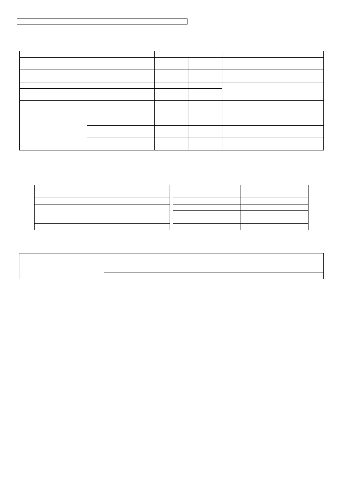
Frequently Used Items (Base Unit)
ex.)
Items Address Default Data New Data Remarks
C-ID (FSK) sensitivity 04 B6 00 01 (6 dB up) 02 (12 dB up) When hex changes from “00” to “01” or “02”,
C-ID (DTMF) sensitivity 04 C4 50 60 (6 dB up) 70 (12 dB up) When hex changes from “50” to “60” or “70”,
Frequency 00 02/00 01 02/70 - - Use these items in a READ-ONLY mode to
ID 00 10~00 14 Given value - -
Bell length 01 F7 32 (5sec) (*3) 1E (3 sec) 14 (2 sec) This is time until bell stops ringing.
PULSE Dial speed
(10PPS -> 20PPS)
03 9F 28 (40 msec)
(*3)
03 A0 3C (60 msec)
(*3)
01 E4 57 (870 msec)
(*3)
13 (20 msec) - This is pulse make time. (Unit:1ms)
1F (30 msec) - This is pulse break time. (Unit:1ms)
2C (440 msec) - This is inter-digit time in pulse mode.
gain increases by 6 dB or 12 dB.
gain increases by 6 dB or 12 dB.
confirm the contents. Careless rewriting may
cause serious damage to the computer system.
(Unit: 100 ms)
(Unit:10ms)
Note:
(*1) Refer to Registering a Handset to a Base Unit (P.20).
(*2) When you enter the address or New Data, please refer to the table below.
Desired Number (hex) Input Keys Desired Number (hex) Input Keys
00 A[R] + 0
11 B[R] + 1
.. C[R] + 2
.. D[R] + 3
.. E[R] + 4
99 F[R] + 5
(*3)
Bell length 32 (hex) = 50 (dec) → 50 × 100 msec = 5000 msec (5 sec)
PULSE Dial speed
(10PPS -> 20PPS)
28 (hex) = 40 (dec) → 40 × 1 msec = → 40 msec → 28 (40 msec)
3C (hex) = 60 (dec) → 60 × 1 msec = 60 msec → 3C (60 msec)
57 (hex) = 87 (dec) → 87 × 10 msec = 870 msec
28
8.1.2. Handset
KX-TG6411CAM/KX-TG6411CAT/KX-TG6412CAM/KX-TG6412CAT/KX-TGA641RUM/KX-TGA641RUT
29
KX-TG6411CAM/KX-TG6411CAT/KX-TG6412CAM/KX-TG6412CAT/KX-TGA641RUM/KX-TGA641RUT
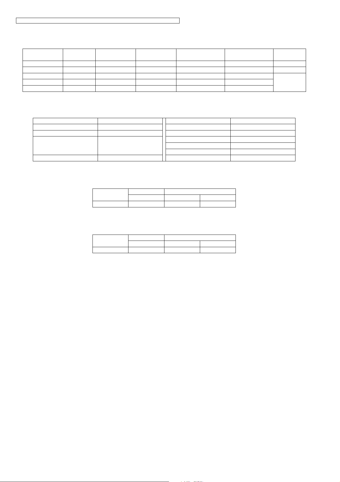
Frequently Used Items (Handset)
ex.)
Items Address Default Data New Data Possible Adjusted
Value MAX (hex)
Sending level 00 06 Adjusted value Given value 6F 00 (*2)
Receiving level 00 07 Adjusted value Given value 00 3F (*3)
Battery Low 00 04 70 - - -
Frequency 00 02/00 01 02/70 - - -
ID 00 10~00 14 Given value - - -
Possible Adjusted
Value MIN (hex)
Note:
(*1) When you enter the address or New Data, please refer to the table below.
Desired Number (hex.) Input Keys Desired Number (hex.) Input Keys
00 A[R] + 0
11 B[R] + 1
.. C[R] + 2
.. D[R] + 3
.. E[R] + 4
99 F[R] + 5
(*2) When adding “01” (hex) to default value, sending level increases by 0.25 dB.
ex.)
Item Default Data New Data
35 39 31
Sending level -10dBm -9dBm -11dBm
(*3) When reducing “01” (hex) from default value, receiving level increases by 0.25 dB.
ex.)
Remarks
(*4)
Item Default Data New Data
18 1C 14
Receiving level -21dBm -22dBm -20dBm
(*4) Use these items in a READ-ONLY mode to confirm the contents. Careless rewriting may cause serious damage to the
handset.
30
 Loading...