

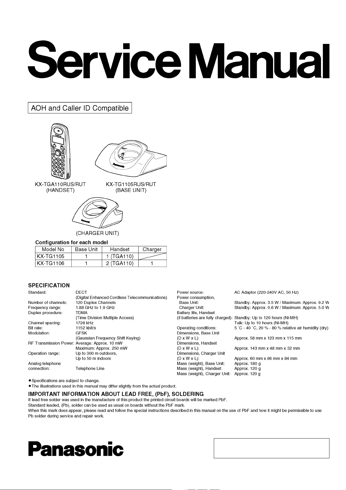
PANASONIC KX-TG1105, KX-TG1106RU, TGA110RU Service Manual
ORDER NO. KM40603006CE
Telephone Equipment
KX-TG1105RUS
KX-TG1105RUT
KX-TG1106RUS
KX-TG1106RUT
KX-TGA110RUS
KX-TGA110RUT
Digital Cordless Phone
Silver Version
Titanium Black Version
(for Russia)
© 2006 Panasonic Communications Co., Ltd. All
rights reserved. Unauthorized copying and
distribution is a violation of law.
KX-TG110 5RUS / KX-TG1105R UT / KX-TG1106R US / KX-TG 1106R UT / KX-TG A110RUS / KX-TGA110RUT
Note:
Because CONTENTS 4 is the extract from the Operating Instructions of this model, it is subject to change without notice. You can
download and refer to the original Operating Instructions on TSN Server for further information.
CONTENTS
Page Page
1 ABOUT LEAD FREE SOLDER (PbF: Pb free) 4
1.1. Suggested PbF Solder
1.2. How to recognize that Pb Free solder is used
2 FOR SERVICE TECHNICIANS
3 CAUTION
4 OPERATING INSTRUCTIONS
4.1. Battery
4.2. Location of Controls
4.3. Connections
4.4. Guide to Settings
4.5. For Service Hint
5 DISASSEMBLY INSTRUCTIONS
5.1. Base Unit
5.2. Handset
5.3. Charger Unit
6 ASSEMBLY INSTRUCTIONS
6.1. Warning When Constructing the Base Unit
6.2. How to Replace the Handset LCD
7 TROUBLESHOOTING GUIDE
7.1. Check Power
7.2. Check Battery Charge
7.3. Check Link
7.4. Check Handset Transmission
7.5. Check Handset Reception
7.6. Check Caller ID
7.7. Bell Reception
8 TROUBLESHOOTING BY SYMPTOM (BASE UNIT AND
CHARGER UNIT)
8.1. Check Point (Base Unit)
8.2. The Setting Method of JIG (Base Unit)
8.3. Adjustment Standard (Base Unit)
8.4. Check Point (Charger Unit)
8.5. Adjustment Standard (Charger Unit)
9 TROUBLESHOOTING BY SYMPTOM (HANDSET)
9.1. Check Point (Handset)
9.2. The Setting Method of JIG (Handset)
9.3. Adjustment Standard (Handset)
10 THINGS TO DO AFTER REPLACING IC
4
5
5
5
6
6
7
8
9
11
12
12
13
14
15
15
16
17
18
19
20
22
22
22
22
23
23
28
30
32
32
33
33
36
38
10.1. Base Unit
10.2. Handset
11 RF SPECIFICATION
11.1. Base Unit
11.2. Handset
12 HOW TO CHECK THE HANDSET SPEAKER
13 FREQUENCY TABLE (MHz)
14 BLOCK DIAGRAM (BASE UNIT)
15 CIRCUIT OPERATION (BASE UNIT)
15.1. Outline
15.2. Power Supply Circuit
15.3. Telephone Line Interface
15.4. Transmitter/Receiver
15.5. Pulse Dialling
16 BLOCK DIAGRAM (HANDSET)
17 CIRCUIT OPERATION (HANDSET)
17.1. Outline
17.2. Power Supply Circuit/Reset Circuit
17.3. Charge Circuit
17.4. Battery Low/Power Down Detector
18 CIRCUIT OPERATION (CHARGER UNIT)
18.1. Power Supply Circuit
19 SIGNAL ROUTE
20 CPU DATA (BASE UNIT)
20.1. IC2 (BBIC)
21 CPU DATA (HANDSET)
21.1. IC4 (BBIC)
22 ENGINEERING MODE
22.1. Base Unit
22.2. Handset
23 EEPROM LAYOUT (BASE UNIT)
23.1. Scope
23.2. Introduction
23.3. EEPROM Layout
24 EEPROM LAYOUT (HANDSET)
24.1. Scope
39
39
39
40
40
40
40
41
42
43
43
44
45
45
45
46
47
47
47
47
47
48
48
49
50
50
52
52
54
54
56
58
58
58
58
61
61
2

KX-TG110 5RUS / KX-TG1105R UT / KX-TG1106R US / KX-TG 1106R UT / KX-TG A110RUS / KX-TGA110RUT
24.2. Introduction 61
24.3. EEPROM contents
25 HOW TO REPLACE THE FLAT PACKAGE IC
25.1. PREPARATION
25.2. FLAT PACKAGE IC REMOVAL PROCEDURE
25.3. FLAT PACKAGE IC INSTALLATION PROCEDURE
25.4. BRIDGE MODIFICATION PROCEDURE
26 CABINET AND ELECTRICAL PARTS (BASE UNIT)
27 CABINET AND ELECTRICAL PARTS (HANDSET)
28 CABINET AND ELECTRICAL PARTS (CHARGER UNIT)
29 ACCESSORIES AND PACKING MATERIALS
29.1. KX-TG1105RUS/RUT
29.2. KX-TG1106RUS/RUT
30 TERMINAL GUIDE OF THE ICs, TRANSISTORS AND DIODES
30.1. Base Unit
30.2. Handset
30.3. Charger Unit
31 REPLACEMENT PARTS LIST
31.1. Base Unit
31.2. Handset
31.3. Charger Unit
61
64
64
64
65
65
66
67
68
69
69
70
31.4. Accessories and Packing Materials
31.5. Fixtures and Tools
32 FOR SCHEMATIC DIAGRAM
32.1. Base Unit (SCHEMATIC DIAGRAM (BASE UNIT))
32.2. Handset (SCHEMATIC DIAGRAM (HANDSET))
32.3. Charger Unit (SCHEMATIC DIAGRAM (CHARGER UNIT))
33 SCHEMATIC DIAGRAM (BASE UNIT)
34 SCHEMATIC DIAGRAM (HANDSET)
35 SCHEMATIC DIAGRAM (CHARGER UNIT)
36 CIRCUIT BOARD (BASE UNIT)
36.1. Component View
36.2. Flow Solder Side View
71
37 CIRCUIT BOARD (HANDSET)
71
71
71
72
72
37.1. Component View
37.2. Flow Solder Side View
38 CIRCUIT BOARD (CHARGER UNIT)
38.1. Component View
38.2. Flow Solder Side View
73
74
74
75
77
77
77
77
78
80
82
83
83
84
85
85
86
87
87
87
3
KX-TG110 5RUS / KX-TG1105R UT / KX-TG1106R US / KX-TG 1106R UT / KX-TG A110RUS / KX-TGA110RUT
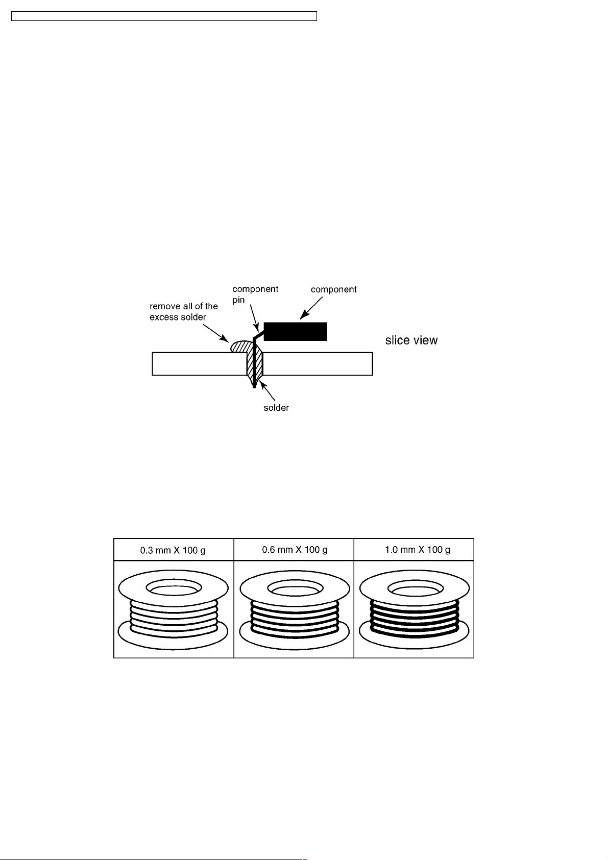
1 ABOUT LEAD FREE SOLDER (PbF: Pb free)
Note:
In the information below, Pb, the symbol for lead in the periodic table of elements, will refer to standard solder or solder that
contains lead.
We will use PbF solder when discussing the lead free solder used in our manufacturing process which is made from Tin (Sn),
Silver (Ag), and Copper (Cu).
This model, and others like it, manufactured using lead free solder will have PbF stamped on the PCB. For service and repair
work we suggest using the same type of solder.
Caution
•
• PbF solder has a melting point that is 50°F ~70°F (30°C ~ 40°C) higher than Pb solder. Please use a soldering iron with
• •
temperature control and adjust it to 700°F ± 20°F (370°C ± 10°C).
•
• Exercise care while using higher temperature soldering irons.: Do not heat the PCB for too long time in order to prevent
• •
solder splash or damage to the PCB.
•
• PbF solder will tend to splash if it is heated much higher than its melting point, approximately 1100°F (600°C).
• •
•
• When applying PbF solder to double layered boards, please check the component side for excess which may flow onto the
• •
opposite side (See the figure below).
1.1. Suggested PbF Solder
There are several types of PbF solder available commercially. While this product is manufactured using Tin, Silver, and Copper
(Sn+Ag+Cu), you can also use Tin and Copper (Sn+Cu) or Tin, Zinc, and Bismuth (Sn+Zn+Bi). Please check the
manufacturer’s specific instructions for the melting points of their products and any precautions for using their product with other
materials. The following lead free (PbF) solder wire sizes are recommended for service of this product: 0.3 mm, 0.6 mm and
1.0 mm.
4
KX-TG110 5RUS / KX-TG1105R UT / KX-TG1106R US / KX-TG 1106R UT / KX-TG A110RUS / KX-TGA110RUT
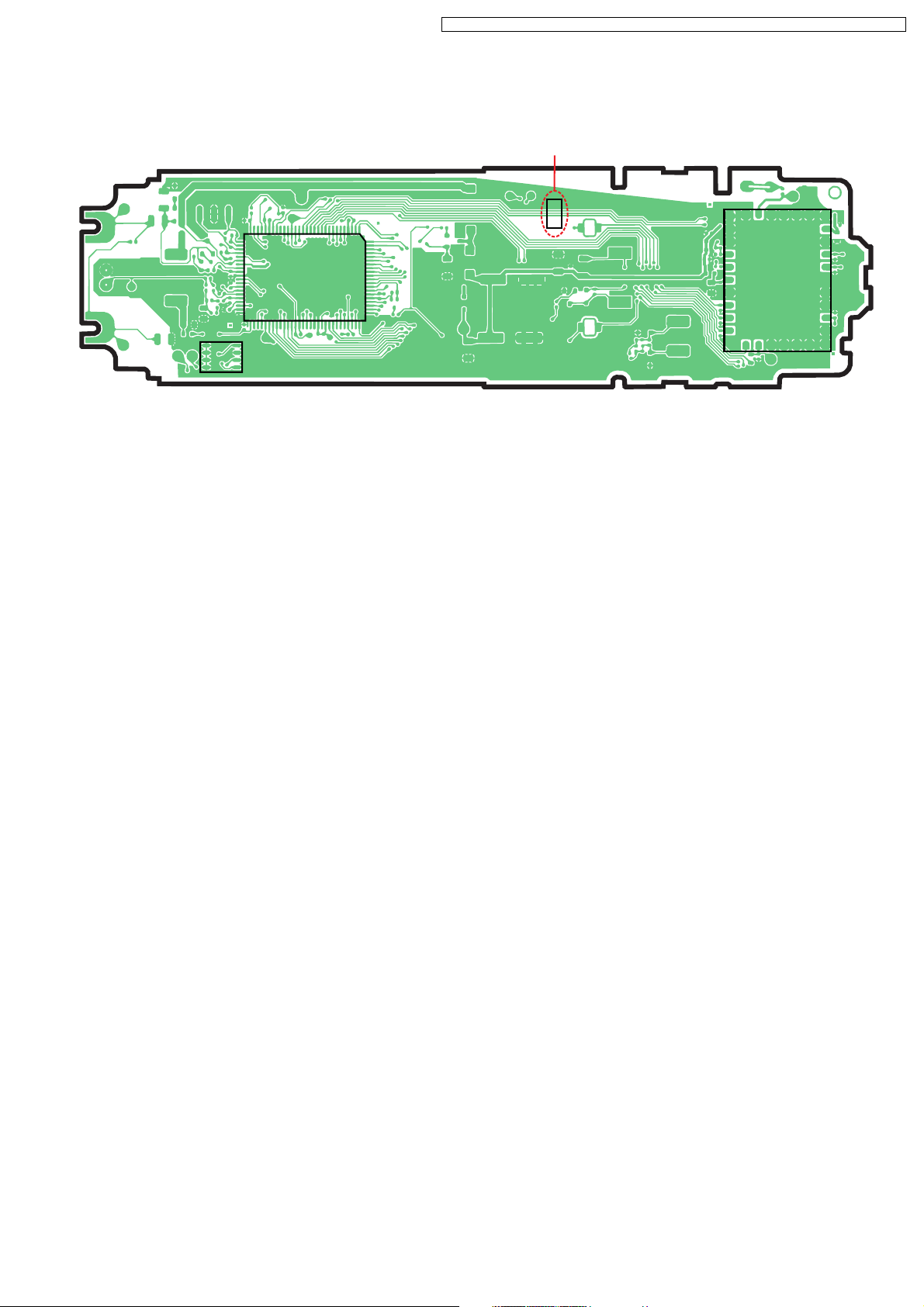
1.2. How to recognize that Pb Free solder is used
(Example: Handset P.C.B.)
Marked
PbF
148
IC2
30
31
IC4
50
51
5
1
100
81
80
(Component View)
Note:
The location of the “PbF” mark is subject to change without notice.
2 FOR SERVICE TECHNICIANS
ICs and LSIs are vulnerable to static electricity.
When repairing, the following precautions will help prevent recurring malfunctions.
1. Cover the plastic parts boxes with aluminum foil and ground them.
2. Ground the soldering irons.
3. Use a conductive mat on the worktable.
4. Do not touch IC or LSI pins with bare fingers.
1
IC3
3 CAUTION
1. Danger of explosion if battery is incorrectly replaced.
2. Replace only with the same or equivalent type recommended by the manufacturer.
3. Dispose of used batteries according to the manufacture’s Instructions.
5
KX-TG110 5RUS / KX-TG1105R UT / KX-TG1106R US / KX-TG 1106R UT / KX-TG A110RUS / KX-TGA110RUT
4 OPERATING INSTRUCTIONS
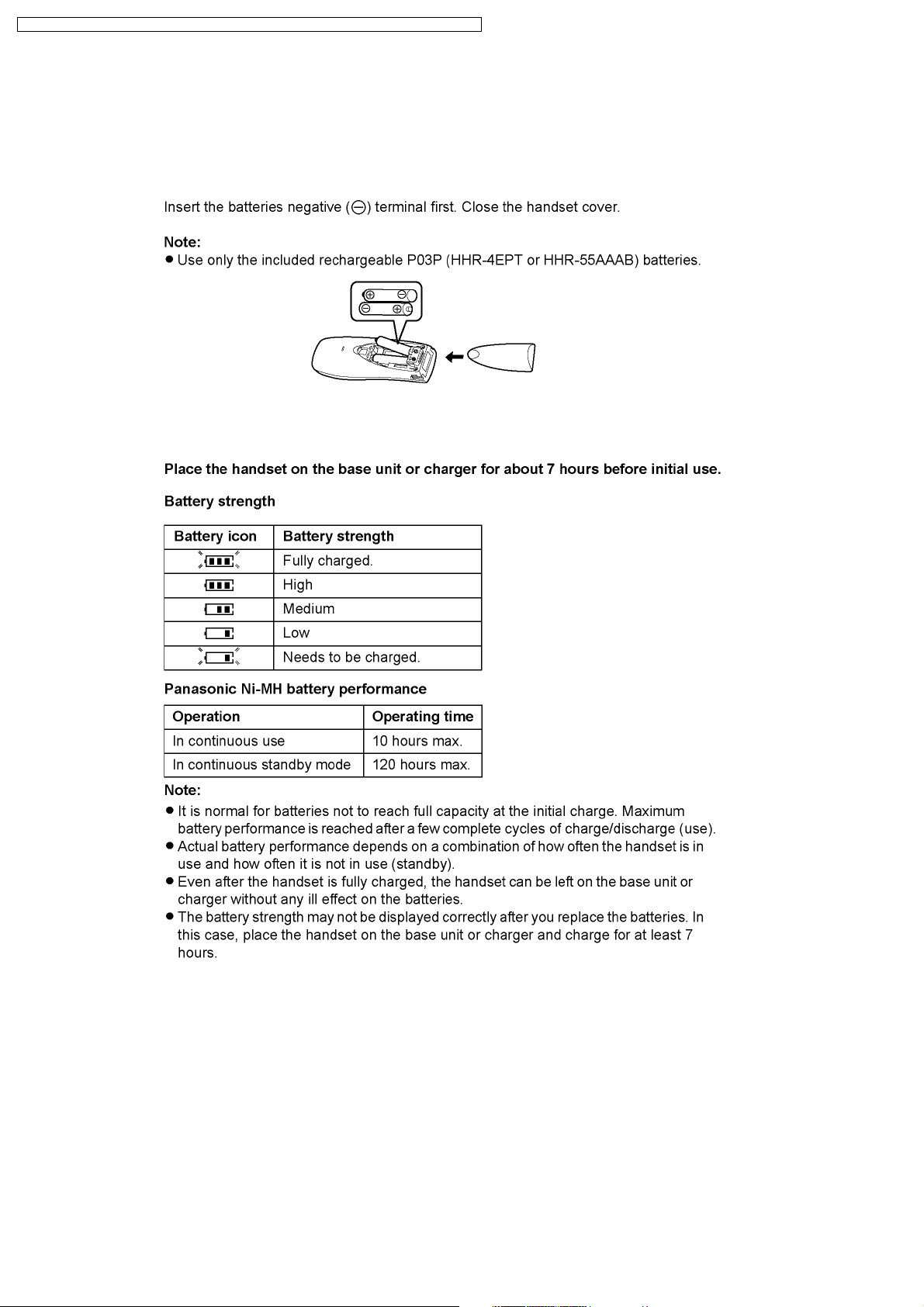
4.1. Battery
4.1.1. Battery Installation
4.1.2. Battery Charge
6
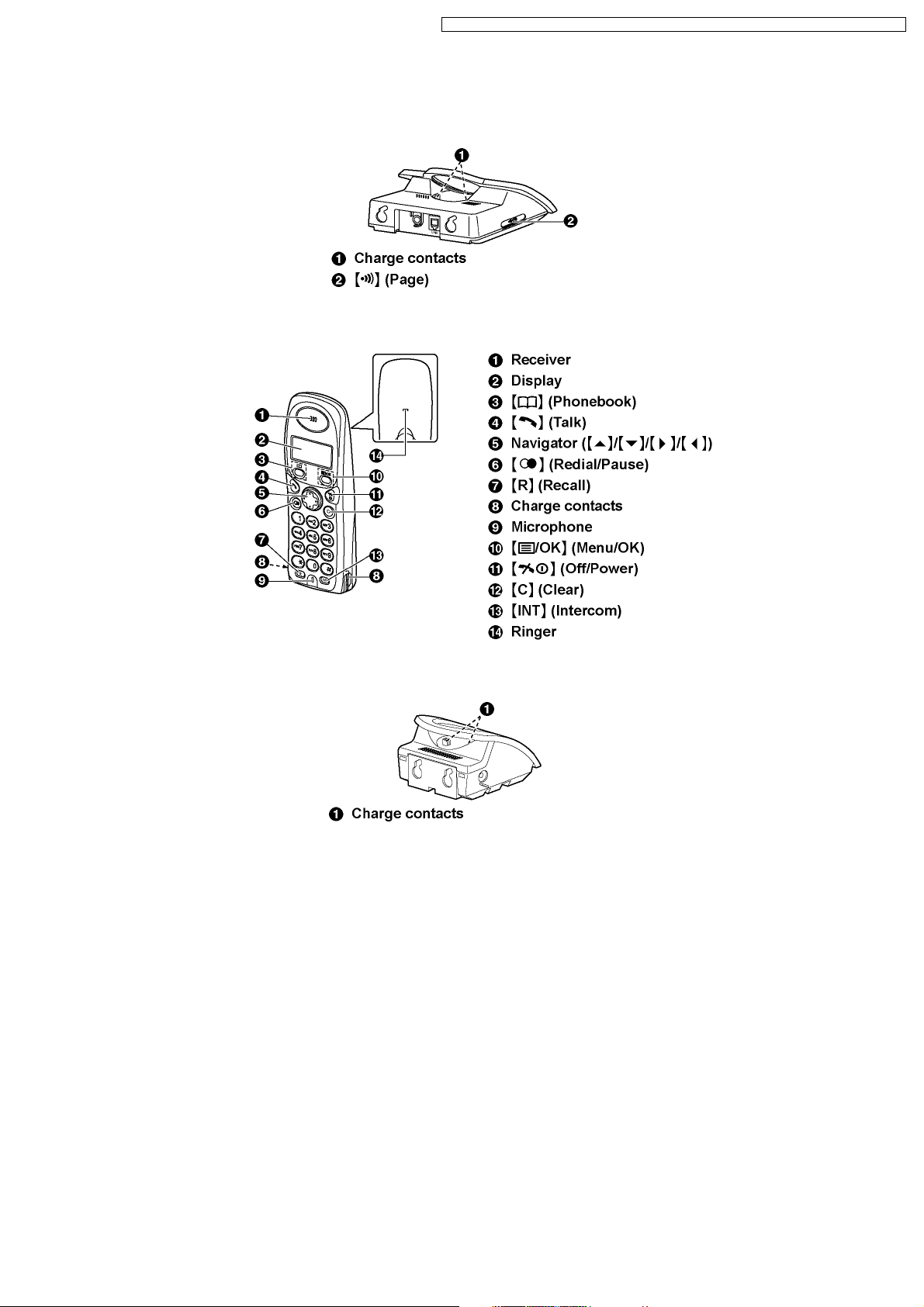
4.2. Location of Controls
4.2.1. Base Unit
4.2.2. Handset
KX-TG110 5RUS / KX-TG1105R UT / KX-TG1106R US / KX-TG 1106R UT / KX-TG A110RUS / KX-TGA110RUT
4.2.3. Charger (KX-TG1106 only)
7
KX-TG110 5RUS / KX-TG1105R UT / KX-TG1106R US / KX-TG 1106R UT / KX-TG A110RUS / KX-TGA110RUT
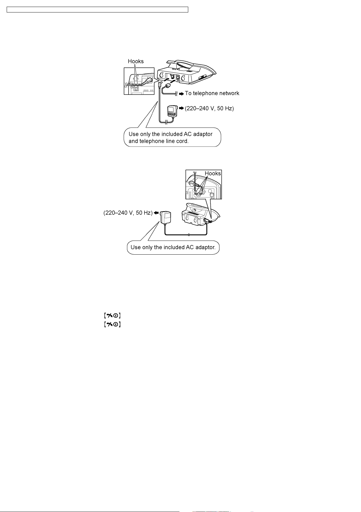
4.3. Connections
4.3.1. Base Unit
4.3.2. Charger (KX-TG1106 only)
Note:
•
• Never install telephone wiring during a lightning storm.
• •
•
• Do not connect the AC adaptor to a ceiling-mounted AC outlet, as the weight of the adaptor may cause it to become
• •
disconnected.
•
• To turn the power on, press
• •
•
• To turn the power off, press
• •
for about 1 second.
for about 2 seconds.
8
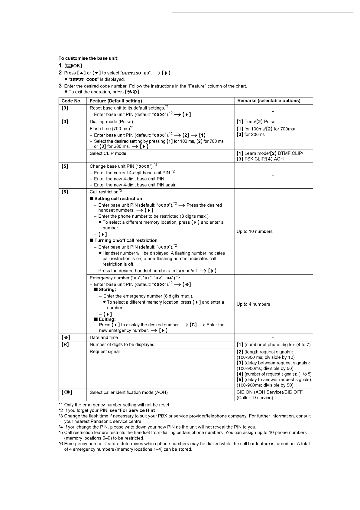
4.4. Guide to Settings
4.4.1. Base Unit
KX-TG110 5RUS / KX-TG1105R UT / KX-TG1106R US / KX-TG 1106R UT / KX-TG A110RUS / KX-TGA110RUT
Cross Reference:
For Service Hint (P.11)
9
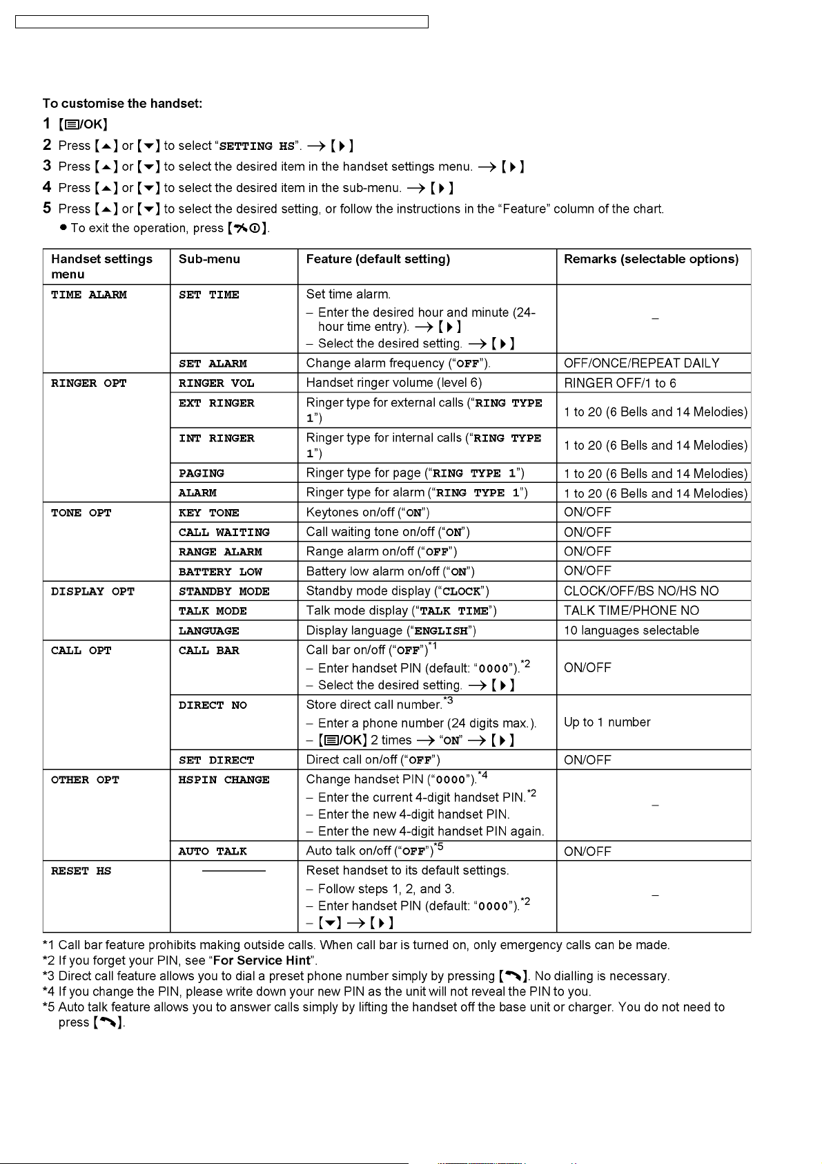
KX-TG110 5RUS / KX-TG1105R UT / KX-TG1106R US / KX-TG 1106R UT / KX-TG A110RUS / KX-TGA110RUT
4.4.2. Handset
Cross Reference:
For Service Hint (P.11)
10
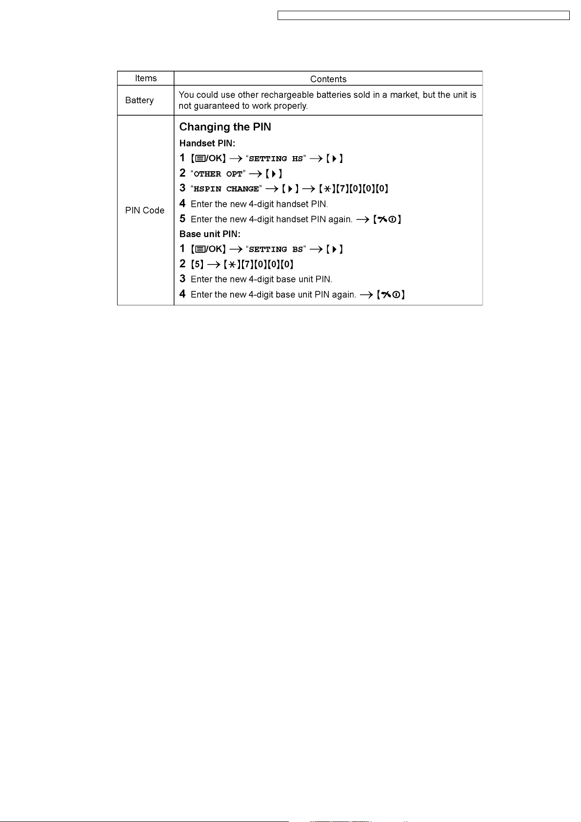
4.5. For Service Hint
KX-TG110 5RUS / KX-TG1105R UT / KX-TG1106R US / KX-TG 1106R UT / KX-TG A110RUS / KX-TGA110RUT
11
KX-TG110 5RUS / KX-TG1105R UT / KX-TG1106R US / KX-TG 1106R UT / KX-TG A110RUS / KX-TGA110RUT
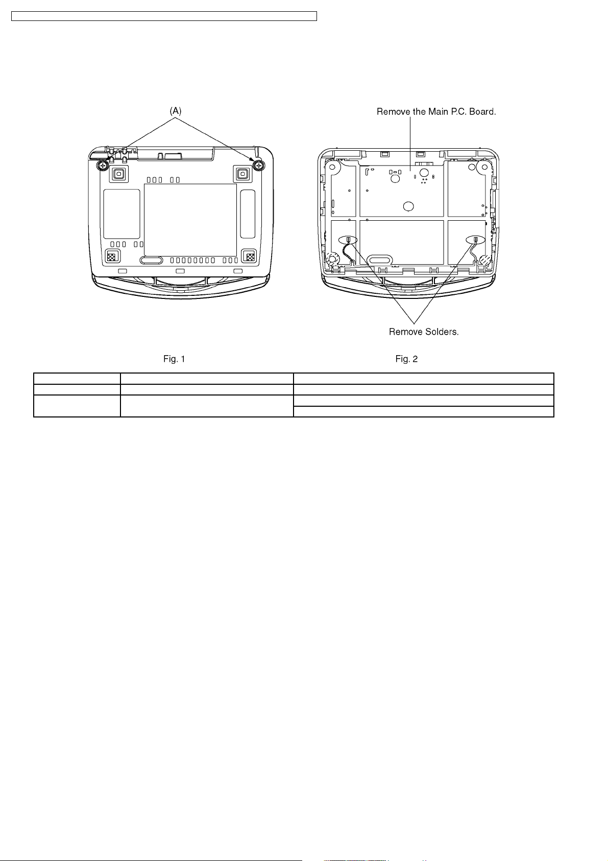
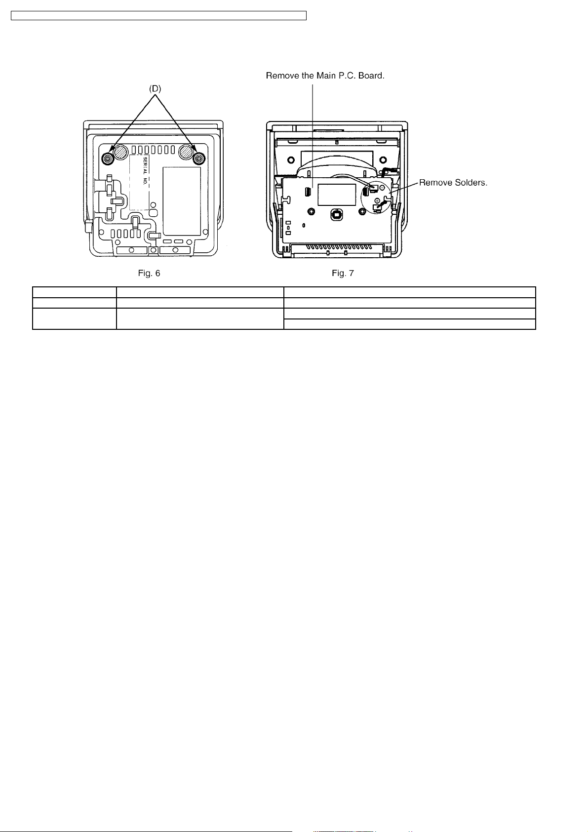
5 DISASSEMBLY INSTRUCTIONS
5.1. Base Unit
Shown in Fig.- To Remove Remove
1 Cabinet Cover Screws (2.6 × 12)..........(A) × 2
2 Main P.C. Board Solders
Main P.C. Board
12
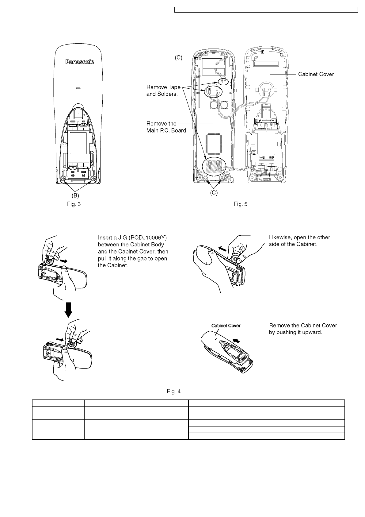
5.2. Handset
KX-TG110 5RUS / KX-TG1105R UT / KX-TG1106R US / KX-TG 1106R UT / KX-TG A110RUS / KX-TGA110RUT
Shown in Fig.- To Remove Remove
3 Cabinet Cover Screws (2 × 8)..........(B) × 2
4 Follow the procedure.
5 Main P.C. Board Screw (2 × 8)..............(C) × 3
Tape and Solders
Main P.C. Board
13
KX-TG110 5RUS / KX-TG1105R UT / KX-TG1106R US / KX-TG 1106R UT / KX-TG A110RUS / KX-TGA110RUT
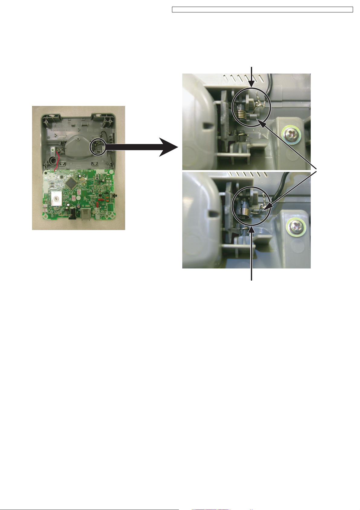
5.3. Charger Unit
Shown in Fig.- To Remove Remove
6 Cabinet Cover Screws (2.6 × 14)..........(D) × 2
7 Main P.C. Board Solders
Main P.C. Board
14
KX-TG110 5RUS / KX-TG1105R UT / KX-TG1106R US / KX-TG 1106R UT / KX-TG A110RUS / KX-TGA110RUT
6 ASSEMBLY INSTRUCTIONS
6.1. Warning When Constructing the Base Unit
CHG terminal is properly fit in the cabinet.
OK
Rib
NG
CHG terminal comes out of rib by pulling black lead wire when opening the cabinet and turning
the PCB over. The terminal cannot have enough elastic force, cannot have good contact with
handset, and it will result in charge problem.
15
KX-TG110 5RUS / KX-TG1105R UT / KX-TG1106R US / KX-TG 1106R UT / KX-TG A110RUS / KX-TGA110RUT
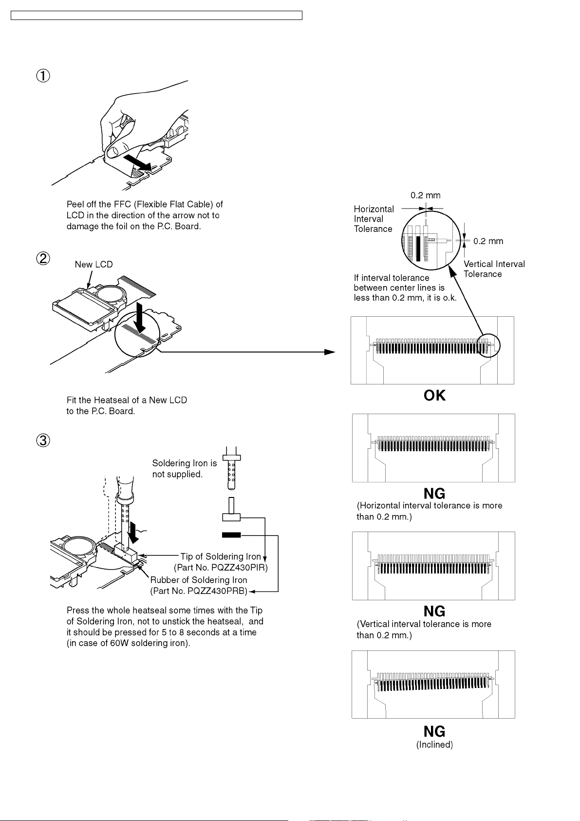
6.2. How to Replace the Handset LCD
16
KX-TG110 5RUS / KX-TG1105R UT / KX-TG1106R US / KX-TG 1106R UT / KX-TG A110RUS / KX-TGA110RUT
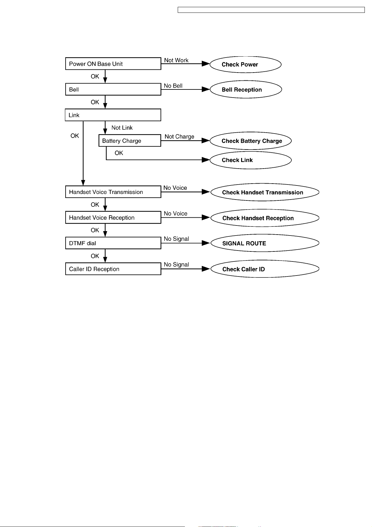
7 TROUBLESHOOTING GUIDE
Flow Chart
Cross Reference:
Check Power (P.18)
Bell Reception (P.22)
Check Battery Charge (P.19)
Check Link (P.20)
Check Handset Transmission (P.22)
Check Handset Reception (P.22)
SIGNAL ROUTE (P.49)
Check Caller ID (P.22)
17
KX-TG110 5RUS / KX-TG1105R UT / KX-TG1106R US / KX-TG 1106R UT / KX-TG A110RUS / KX-TGA110RUT
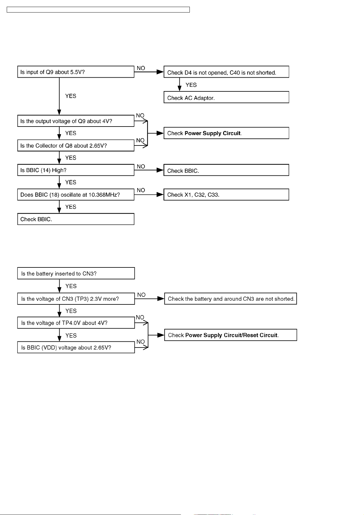
7.1. Check Power
7.1.1. Base Unit
Is the AC Adaptor inserted into AC outlet? (Check AC Adaptor’s specification.)
Cross Reference
Power Supply Circuit (P.44)
7.1.2. Handset
Cross Reference
Power Supply Circuit/Reset Circuit (P.47)
Note:
BBIC is IC2.
Note:
BBIC is IC4.
18
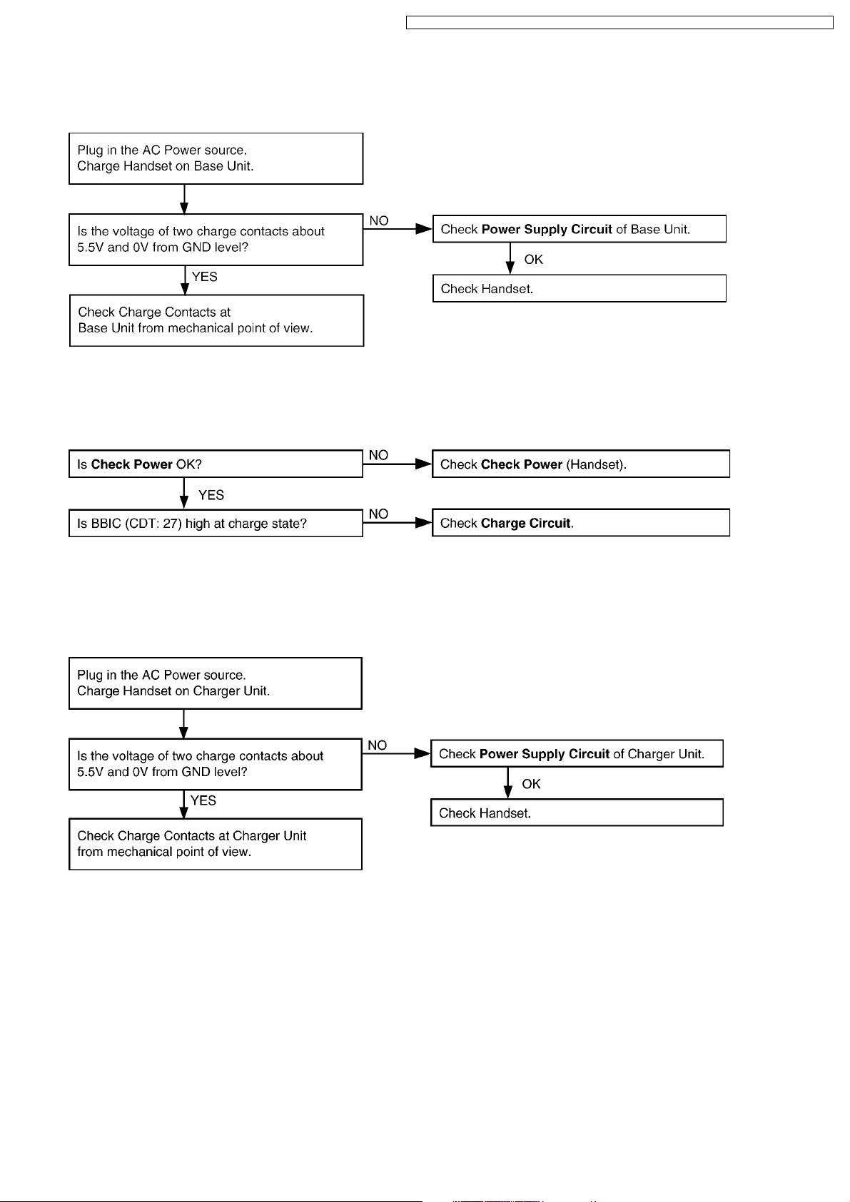
7.2. Check Battery Charge
7.2.1. Base Unit
Cross Reference:
Power Supply Circuit (P.44)
7.2.2. Handset
KX-TG110 5RUS / KX-TG1105R UT / KX-TG1106R US / KX-TG 1106R UT / KX-TG A110RUS / KX-TGA110RUT
Cross Reference:
Check Power (P.18)
Charge Circuit (P.47)
7.2.3. Charger Unit
Cross Reference:
Power Supply Circuit (P.48)
Note:
BBIC is IC4.
19
KX-TG110 5RUS / KX-TG1105R UT / KX-TG1106R US / KX-TG 1106R UT / KX-TG A110RUS / KX-TGA110RUT
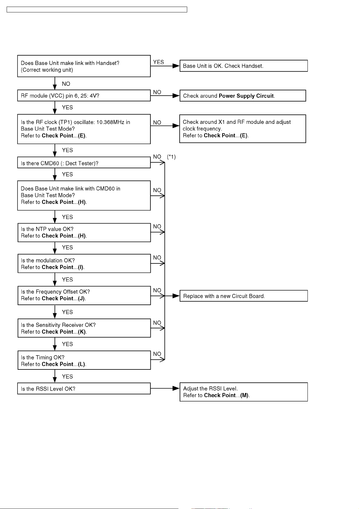
7.3. Check Link
7.3.1. Base Unit
Cross Reference:
Power Supply Circuit (P.44)
Check Point (Base Unit) (P.23)
Note:
(*1) Refer to TROUBLESHOOTING BY SYMPTOM (BASE UNIT AND CHARGER UNIT) (P.23).
20
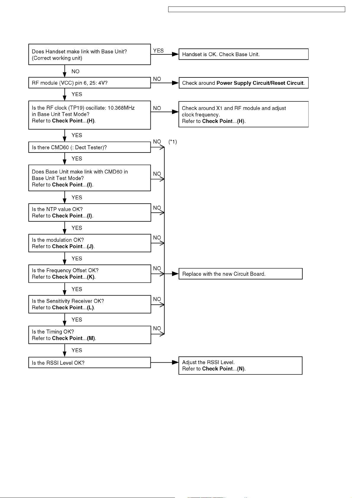
7.3.2. Handset
KX-TG110 5RUS / KX-TG1105R UT / KX-TG1106R US / KX-TG 1106R UT / KX-TG A110RUS / KX-TGA110RUT
Cross Reference
Power Supply Circuit/Reset Circuit (P.47)
Check Point (Handset) (P.33)
Note:
(*1) Refer to TROUBLESHOOTING BY SYMPTOM (HANDSET) (P.33).
21
KX-TG110 5RUS / KX-TG1105R UT / KX-TG1106R US / KX-TG 1106R UT / KX-TG A110RUS / KX-TGA110RUT
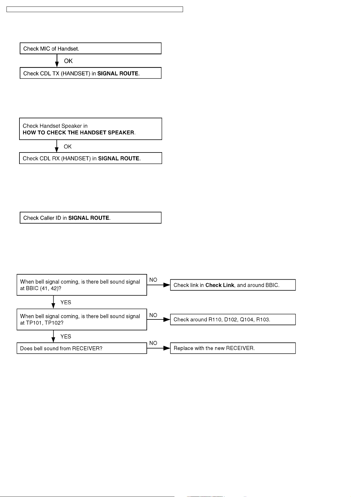
7.4. Check Handset Transmission
Cross Reference:
SIGNAL ROUTE (P.49)
7.5. Check Handset Reception
Cross Reference:
HOW TO CHECK THE HANDSET SPEAKER (P.40).
SIGNAL ROUTE (P.49)
7.6. Check Caller ID
Cross Reference:
SIGNAL ROUTE (P.49)
7.7. Bell Reception
7.7.1. Handset
Cross Reference:
Telephone Line Interface (P.45)
Check Link (P.20)
HOW TO CHECK THE HANDSET SPEAKER (P.40)
Note:
BBIC is IC4.
22
KX-TG110 5RUS / KX-TG1105R UT / KX-TG1106R US / KX-TG 1106R UT / KX-TG A110RUS / KX-TGA110RUT
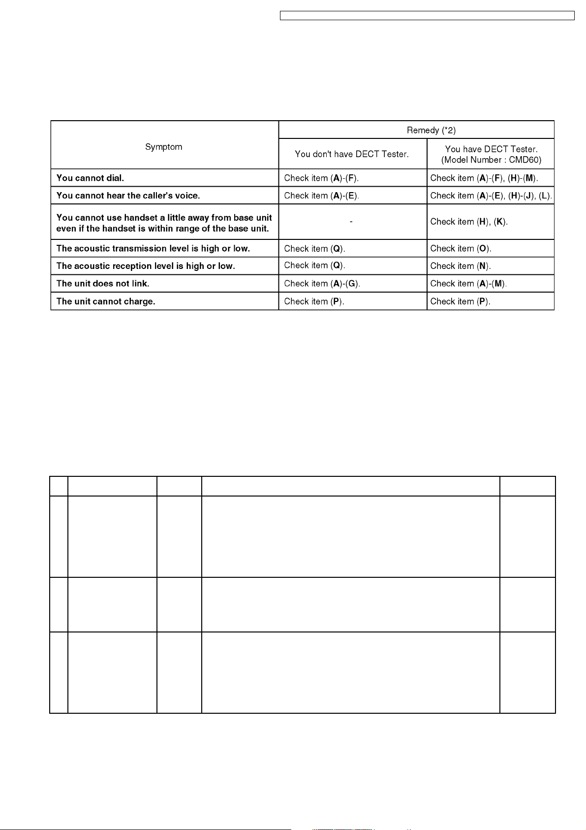
8 TROUBLESHOOTING BY SYMPTOM (BASE UNIT AND
CHARGER UNIT)
If your unit has below symptoms, follow the instructions in remedy column. Remedies depend on whether you have DECT tester
(*1) or not.
Note:
(*1) A general repair is possible even if you don’t have the DECT tester because it is for confirming the levels, such as Acoustic
level in detail.
(*2) Refer to Check Point (Base Unit) (P.23)
8.1. Check Point (Base Unit)
Please follow the items below when BBIC or EEPROM is replaced.
Note:
After the measuring, suck up the solder of TP.
*: PC Setting (P.28) is required beforehand.
The connections of simulator equipments are as shown in Adjustment Standard (Base Unit) (P.30).
Items Adjustment
(A) 2.65V Supply
Confirmation
(B) 4.0V Supply
Confirmation
(C) VBACK Status
Confirmation
Point
- 1. Confirm that the voltage between TP187 and GND is 2.65V ± 0.2V. IC2, Q8, C23,
- 1. Confirm that the voltage between TP91 and GND is 4.0V ± 0.2V. D4, C40, Q9,
- 1. Confirm that the voltage between J102 and GND is 0V ± 0.4V. IC2, Q8, C23,
Procedure Check or
Replace Parts
C24, C25,
C31, C26,
C27, C38,
R33, R36, D5,
C41, R41,
R42, Q9, C40,
D4, X1, C32,
C33, C36, C37
R41, R42,
C41, D5, C75,
C78, C69,
C66, C67,
C76, IC3
C24, C25,
C31, C26,
C27, C38,
R33, R36, D5,
C41, R41,
R42, Q9, C40,
D4, R33, X1,
C32, C33
23
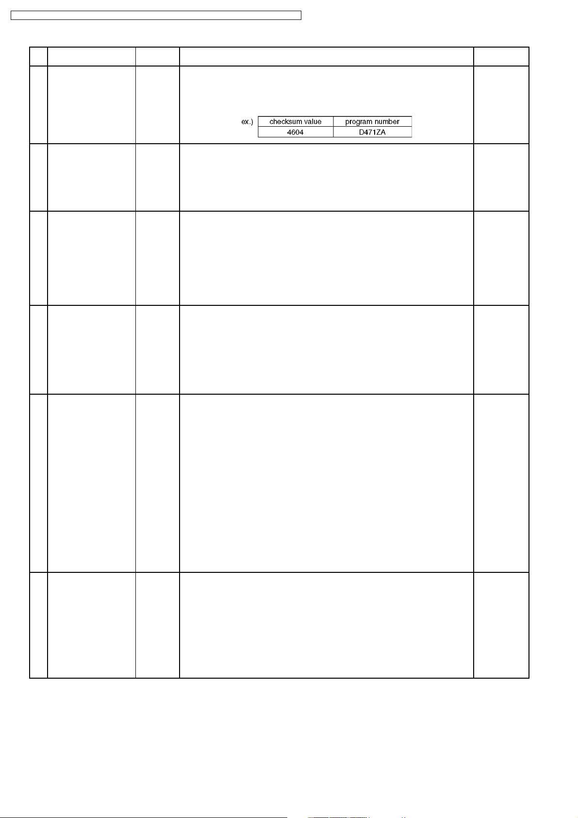
KX-TG110 5RUS / KX-TG1105R UT / KX-TG1106R US / KX-TG 1106R UT / KX-TG A110RUS / KX-TGA110RUT
Items Adjustment
Procedure Check or
Point
(D)* BBIC Confirmation - 1. BBIC Confirmation (Execute the command “getchk”).
2. Confirm the returned checksum value.
Connection of checksum value and program number is shown below.
(E)* BBIC Clock Adjustment
(Important)
TP1 1. Execute the command “deactmac”.
2. Execute the command “conttx”.
3. Input Command “rdeeprom 00 00 02”, then you can confirm the current value.
4. Adjust the frequency of TP1 executing the command “setfreq00xx(wherexx
is the value)” so that the reading of the frequency counter is 10.368000MHz ±
10Hz.
(F)* Hookswitch Check with
DC Characteristics
- 1. Connect J1 (Telephone Socket) to Tel-simulator which is connected with 600
Ω.
2. Set line voltage to 48V at on-hook condition and line current to 40mA at offhook condition of normal telephone.
3. Execute the command “hookoff”.
4. Confirm that the line current is 40mA ± 5mA.
5. Execute the command “hookon”.
6. Confirm that the line current is 0mA + 2mA.
(G)* DTMF Generator Check - 1. Connect J1 (Telephone Socket) to DTMF tester.
2. Execute the command “hookoff” and “dtmf_up”.
3. Confirm that the high frequency (1477.06Hz) group is -3 ± 2dBm.
4. Execute the command “dtmf_lo”.
5. Confirm that the low frequency (852.05Hz) group is -6 ± 2dBm.
(H)* Transmitted Power
Confirmation
- Remove the Antenna before starting steps from 1 to 5.
1. Configure the DECT tester (CMD60) as follows;
<Setting>
•
• Short TP10 and GND
• •
(After the checking, disconnect the wiring between them.)
•
• Test mode: FP
• •
•
• Traffic Channel: 5
• •
•
• Traffic Slot: 4
• •
•
• Mode: Loopback
• •
•
• PMID: 00000
• •
2. Execute the command “testmode”.
3. Initiate connection from DECT tester. (“set up connect”)
4. Execute the command “ANT 1”.
5. Confirm that the NTP value at ANT is 20dBm ~ 25dBm.
(I)* Modulation Check and
Adjustment
ANT Follow steps 1 to 3 of (H) above.
4. Confirm that the B-Field Modulation is 340kHz/div ~ 402kHz/div using data
type Fig31.
5. Adjust the B-Field Modulation if required. (Execute the command “readmod”
and “wrtmod xx”, where xx is the value.)
Replace Parts
IC2, X1, C32,
C33
IC2, IC3, L1,
C48, X1, C32,
C33, L5
IC2, R7, R8,
R9, R10, R77,
Q2, Q3, D2,
C1, C2
IC2, R32, C22,
R23, C80,
C14, C13, Q6,
R22, R21,
R19, R20,
C12, D2, C1,
C2, R77, D3,
R12, Q2, R7,
R8, R9, R10,
Q3
IC2, IC3, L1,
C43, C78,
C75, C69,
C48, C72,
C66, C67,
C76, C57,
C73, L3, DA1,
R66, R67,
C55, C56,
R78, R79,
C54, C58,
C86, R38
IC2, IC3, L1,
C43, C78,
C75, C69,
C48, C72,
C66, C67,
C76, C57,
C73, L3, DA1,
R66, R67,
C55, C56,
R78, R79,
C54, C58,
C86, R38
24
KX-TG110 5RUS / KX-TG1105R UT / KX-TG1106R US / KX-TG 1106R UT / KX-TG A110RUS / KX-TGA110RUT
Items Adjustment
Point
(J)* Frequency Offset Check - Follow steps 1 to 3 of (H).
4. Confirm that the frequency offset is -50kHz ~ +50kHz.
(K)* Sensitivity Receiver
Confirmation
- Follow steps 1 to 3 of (H).
4. Set DECT tester power to -88dBm.
5. Confirm that the BER is < 1000ppm.
(L)* Timing Confirmation - Follow steps 1 to 3 of (H).
4. Confirm that the Timing accuracy is < ± 2.0ppm.
(M)* RSSI Level
Confirmation
- Follow steps 1 to 3 of (H).
4. Set DECT tester power to -88dBm.
5. Execute the command “readrssi”.
6. Confirm: 25 < returned value < 43 (hex) (34 ± F (hex))
Procedure Check or
Replace Parts
IC2, IC3, L1,
C43, C78,
C75, C69,
C48, C72,
C66, C67,
C76, C57,
C73, L3, DA1,
R66, R67,
C55, C56,
R78, R79,
C54, C58,
C86, R38
IC2, IC3, L1,
C43, C78,
C75, C69,
C48, C72,
C66, C67,
C76, C57,
C73, L3, DA1,
R66, R67,
C55, C56,
R78, R79,
C54, C58,
C86, R38
IC2, IC3, L1,
C43, C78,
C75, C69,
C48, C72,
C66, C67,
C76, C57,
C73, L3, DA1,
R66, R67,
C55, C56,
R78, R79,
C54, C58,
C86, R38
IC2, IC3, L1,
C43, C78,
C75, C69,
C48, C72,
C66, C67,
C76, C57,
C73, L3, DA1,
R66, R67,
C55, C56,
R78, R79,
C54, C58,
C86, R38
25

KX-TG110 5RUS / KX-TG1105R UT / KX-TG1106R US / KX-TG 1106R UT / KX-TG A110RUS / KX-TGA110RUT
Items Adjustment
Procedure Check or
Point
(N)* Receive Audio Check
and Adjustment
ANTJ1 1. Configure the DECT tester (CMD60) as follows;
<Setting>
•
• Test mode: FP
• •
•
• Mode: Low
• •
•
• PMID: 00000
• •
2. Execute the command “testmode”.
3. Initiate connection from DECT tester.
4. Execute the command “hookoff”.
5. Execute the command “openau”.
6. Connect J1 (Telephone Socket) to Tel-simulator which is connected with 600
Ω.
7. Set line voltage to 48V and line current to 40mA.
8. Connect DECT tester to Tel-simulator.
9. Input audio signal (200mVrms/1kHz tone) to Tel-simulator.
<DECT tester setting>
•
• Scramble: On
• •
•
• AF Gen. to ADPCM: Off
• •
•
• AF Meter Input: ADPCM
• •
•
• AF Gen. Frequency: 1000Hz
• •
•
• AF Gen. Level: 200mVrms
• •
10. Confirm hearing tone: 350mVrms ± 100mVrms
11. Adjust audio level if required. (Make sure current value using “getmicgain”.And
then execute the command “setmicgain xx”, where xx is the value.)
12. Confirm that the B-field audio distortion with DECT tester is < 5%.
(O)* Transmit Audio Check
and Adjustment
ANTJ1 1. Configure the DECT tester (CMD60) as follows;
<Setting>
•
• Test mode: FP
• •
•
• Mode: Low
• •
•
• PMID: 00000
• •
2. Execute the command “testmode”.
3. Initiate connection from DECT tester.
4. Execute the command “hookoff”.
5. Execute the command “openau”.
6. Connect J1 (Telephone Socket) to Tel-simulator which is connected with 600
Ω.
7. Set line voltage to 48V and line current to 40mA.
8. Input audio signal (30mVrms/1kHz tone) to DECT tester.
<DECT tester setting>
•
• Scramble: On
• •
•
• AF Gen. to ADPCM: On
• •
•
• AF Meter Input: AF Voltm
• •
•
• AF Gen. Frequency: 1000Hz
• •
•
• AF Gen. Level: 30mVrms
• •
9. Confirm hearing tone: 380mVrms ± 100mVrms.
10. Adjust audio level if required. (Make sure current value using “getspkrgain”.
And then execute the command “setspkrgain xx”, where xx is the value.)
11. Confirm that the audio distortion at 600R of Tel-simulator is < 5%.
(P) Charging Check - 1. Connect Charge Contact 12Ω/2W resistor between charge+ and charge-.
2. Measure and confirm voltage across the resistor is 2.3V ± 0.2V.
Replace Parts
IC2, C21, R31,
C20, C11,
R18, R16, D3,
R12, Q2, R7,
R8, Q3, R9,
R10, D2, C1,
C2, R77, IC3,
L1, C43, C78,
C75, C69,
C48, C72,
C66, C67,
C76, C57,
C73, L3, DA1,
R66, R67,
C55, C56,
R78, R79,
C54, C58,
C86, R38
IC2, R32, C22,
R23, C80,
C14, C13,
R22, R21, Q6,
R18, R19,
R20, C12, D2,
C1, C2, R77,
R16, D3, R12,
Q2, R7, R8,
R9, R10, Q3,
IC3, L1, C43,
C78, C75,
C69, C48,
C72, C66,
C67, C76,
C57, C73, L3,
DA1, R66,
R67, C55,
C56, R78,
R79, C54,
C58, C86, R38
D4, R43, R44
26

KX-TG110 5RUS / KX-TG1105R UT / KX-TG1106R US / KX-TG 1106R UT / KX-TG A110RUS / KX-TGA110RUT
Items Adjustment
Point
(Q)* Audio Check - 1. Link with Handset.
2. Set line voltage to 48V and line current to 40mA.
3. Input -45dBm/1kHz to MIC of Handset.
Measure the Level at Line I/F and distortion level.
4. Confirm that the level is -7.5 ± 2dBm and that the distortion level is < 5% at
TEL Line (600Ω Load).
5. Input -20dBm/1kHz to Line I/F.
Measure the level at Receiver of Handset and distortion level
(*Receive volume set to second position from minimum).
6. Confirm that the level is -23 ± 2dBm and that the distortion level is < 5% at
Receiver (vol = Low, 150Ω Load).
Procedure Check or
Replace Parts
27
 Loading...