

Page 1
Service Seminar
Service Seminar
(Circuit Explanation of LCD for Latin America)
(Circuit Explanation of LCD for Latin America)
Model
Model
DATE
DATE
: TC-32/26LX600
: TC-32/26LX600
: Oct 23-24, 2006
: Oct 23-24, 2006
TC-32/26LX60
TC-32/26LX60
TC-23LX60
TC-23LX60
CS Promotion Center
Panasonic AVC Networks Company
Page 2

Contents
<Review of E-Seminar>
1. LCD Line-up for Y2006
2. Chassis Structure
3. Explanation for Signal Circuit
4. Explanation for Power Supply Circuit
5. Troubleshooting
Page 3

Contents
<Hands on for LCD>
1. Typical Trouble Example
2. The Idea of Diagnosis for LCD
3. Introduction of Jig
Page 4

<Review of E-Seminar>
Page 5

1. LCD Line-up for Y2006
Page 6
1-1-1. LCD Line-up for Y2006 (USA)
2005
32LX50
26LX50
23LX50
19LX50
26LE55
23LE55
23LE50
STEP UP
LEADER
Derivative Model
2006
TC-32LX600
TC-26LX600
TC-32LX60
TC-26LX60
TC-23LX60
TC-32LE60
TC-26LE60
19LE50
20LA5
20LE50
20LE5
4:3
Page 7
1-1-2. LCD Line-up for Y2006 (Canada)
2005
32LX50
26LX50
23LX50
19LX50
STEP UP
LEADER
2006
TC-32LX600
TC-26LX600
TC-32LX60C
TC-26LX60C
TC-23LX60
23LE50
20LA5
20LE50
20LE5
Derivative Model
/ 4:3 Model
TC-32LE60
TC-26LE60
Page 8

1-1-3. LCD Line-up for Y2006 (Latin America)
2005
32LX50
26LX50
19LX50
20LA5
2006
TC-32LX60L
LEADER
TC-26LX60L
4:3 Model
Page 9
1-1-4. LCD Line-up for Y2006 (Mexico)
2005
32LX50
26LX50
19LX50
20LA5
2006
TC-32LX60C
LEADER
TC-26LX60C
4:3 Model
Page 10
1-2. Product Summary
Screen Size
ATSC
Panel
Video Processor
PC input
LX50
32/26/23/19
―
VA panel
GC4PRO(32/26)
GC3FM(23/19)
―
LX60C/L
32/26
No
IPS Panel
Micronas VCTP *
――POD (CATV)
――SD card
―
LX60
32/26/23
Yes (except 23”)
IPS Panel
Micronas VCTP *
―
―
―
LX600
32/26
Yes
IPS plus panel
Micronas VCTP *
w/ Vivid mode
―
―
―
HDMI
Cosmetic
Color
Others
1 (32/26)
LX50 design
Gray
1 (w/HDAVI **)
LX60 design
Black & silver
* Video-Controller-Text Progressive ** Not available in LX60L
1 (w/HDAVI)
LX60 design
Black & silver
2 (w/HDAVI)
LX60 design
All Black
Demo mode
Page 11

2. Chassis Structure
Page 12

2-1. Location of PC board
SP
Inverter
SP
Current 32/26LX50
P
DG
DV
(HDMI)
AP
H
G
V
SP
K
New LX600/LX60
Control Unit
AP
SP
G
Inverter
SP
32”/26”only 23” only
32/26/LX600, 32/26LX60 only
A
(HDMI)
DT
P
SP
V
K
Differences from LX50:
1. DT board is introduced. (32/26LX600, 32/26LX60 only)
2. The function of DG, H, and DV board are combined to A board.
3. The location of G board, AP board and P board are changed.
Page 13
2-2. Function of PC board
FunctionBoard Name
Digital TunerDT
32/26LX600
32/26LX60
Yes
Yes
Yes
Yes
Yes
Yes
Yes
32/26LX60C
32/26LX60L
23LX60
YesYesMAIN (Signal Processor, HDMI)A
YesYesPower (Board Change Only)P
YesYesDC-DC ConverterAP
YesAV3 Terminal, HeadphoneG
YesHeadphoneK
YesYesLED, Remote ReceiverV
YesYesKEYSCAN, Power SWControl Unit
Page 14

3. Explanation for Signal Circuit
Page 15
3-1. Differences from Current Models
Current 32/26LX50
DG
H
MPU
AUDIO
SWITCH
LVDS
GC4L
GC4
PRO
SOUND
CONTROL
Differences from LX50:
DV
VIDEO
SWITCH
HDMI
A
AUDIO
SWITCH
New LX600
New LX60
FPGA
VCTP
HDMI
(CEC)
* 32/26/LX600, 32/26LX60 only
DT*
ATSC
1. The function of H, DG, and DV board is merged into A board.
2. VCTP and FPGA are introduced instead of VIDEO SW, SOUND CONTROL,
MPU, GC4PRO, GC4L and LVDS as shown in yellow color.
3. DT board is introduced. (32/26LX600, 32/26LX60 only)
4. CEC circuit for HDAVI Control is added on A board. (except 32/26LX60L)
Page 16
3-2-1. Video Signal Flow (LX600/LX60 except 23LX60)
LX600 only
A
DT
TUNER
IC8211
ATSC
LSI
HDMI1
HDMI2
IC8240
PEAKS
LITE
IC5004
HDMI
I/F
Included OSD
Y/C
(for Monitor Out)
Digital
IC4801
DT_VOUTENB
IC4001
OSD
VCTP
OSD
Analog
Digital
AV1
AV2
COMPONENT
Monitor Out
G AV3
Analog
(*) LVDS : Low Voltage Differential Signaling
VIDEO
SWITCH
VIDEO
PROCESSOR
LVDS
LVDS
IC????
IC4004
FPGA
LCD
Panel
LVDS
Page 17
3-2-2. Video Signal Flow (32/26LX60C/L)
A
TUNER
AV1
AV2
COMPONENT
HDMI
Analog
IC5004
HDMI
I/F
Analog
Digital
Digital
IC4001
OSD
VCTP
OSD
VIDEO
PROCESSOR
VIDEO
SWITCH
Monitor Out
G AV3
IC????
IC4004
LVDS
FPGA
LCD
Panel
LVDS
(*) LVDS : Low Voltage Differential Signaling
LVDS
Page 18
3-2-3. Video Signal Flow (23LX60)
A
TUNER
AV1
AV2
COMPONENT
HDMI
Analog
IC5004
HDMI
I/F
Analog
Digital
Digital
IC4001
OSD
VCTP
OSD
VIDEO
PROCESSOR
VIDEO
SWITCH
Monitor Out
G AV3
IC????
IC4004
LVDS
FPGA
LCD
Panel
LVDS
(*) LVDS : Low Voltage Differential Signaling
LVDS
Page 19

3-3-1. Audio Signal Flow (LX600/60 except 23LX60)
LX600 only
IC4001
A
DT
TUNER
Digital
Audio OUT
IC8211
ATSC
LSI
HDMI1
HDMI2
IC8240
PEAKS
LITE
IC8200
Audio
DAC
IC5004
HDMI I/F
IC8232
Audio
SW
IC8244
Audio
ADC
L/R
VCTP
MSP
SW
IC2006
L/R
L/R
IC2001
Audio
AMP
IC2005
HP
AMP
L/R
Analog
Digital
L
R
AV1
AV2
DVI (Analog)
Audio In
Monitor Out
G AV3
Headphone
L/R
L/R
L/R
L/R
L/R
L/R
L/R
AUDIO
SWITCH
Page 20
3-3-2. Audio Signal Flow (32/26LX60C/L)
A
TUNER
AV1
AV2
DVI (Analog)
HDMI
IC2202
IC5004
HDMI I/F
L/R
L/R
L/R
L/R
IC4001
VCTP
MSP
SW
IC2006
AUDIO
SWITCH
L/R
L/R
L/R
L/R
IC2001
Audio
AMP
IC2005
HP
AMP
Analog
Digital
L
R
L/R
Audio In
Monitor Out
G AV3
Headphone
L/R
L/R
L/R
Page 21
3-3-3. Audio Signal Flow (23LX60)
A
TUNER
AV1
AV2
DVI (Analog)
HDMI
IC2202
IC5004
HDMI I/F
L/R
L/R
L/R
L/R
IC4001
VCTP
MSP
SW
IC2006
AUDIO
SWITCH
L/R
L/R
L/R
L/R
IC2001
Audio
AMP
IC2005
HP
AMP
Analog
Digital
L
R
L/R
Audio In
Monitor Out
K AV3
Headphone
L/R
L/R
L/R
Page 22

4. Explanation for Power Supply Circuit
Page 23
4-1. Differences in Power Supply
The Function of P and AP board
P board function
1. AC input
2. Standby circuit
3. Circuit for Inverter and for AP board’s regulator
AP board function
1. Regulator circuit (DC-DC conversion)
Differences of Power Supply in LX600 and all LX60 models
Voltages
P board output
AP board output for Tuner
32/26LX600
32/26LX60
24V
10V
STB7V
30V
MAIN 9V
MAIN5V
18.5V
32/26LX60C
24V
10V
STB7V
30V
MAIN5V
18.5V
24V
STB7V
30V
MAIN5V
23LX6032/26LX60L
120V100V~240V120V120VAC voltage
24V
33V
STB7V
30V
MAIN5V
16.5V18.5VAP board output for Audio AMP
Page 24
4-2-1. Power Supply Outline (LX600/LX60 except 23LX60)
A12
51-53
54,57
A1
4
7
STB 3.3V
MAIN 3.3V
MAIN 2.5V
MAIN 1.5V
MAIN 1.8V
MAIN 3.3V
MAIN 5V
CN1
3
1
P
SUB_ON
Line
Filter
MAIN
Trans
Relay
24V
10V
RELAY
STB
Trans
STB_7V
Relay
24V
CN3
1-3
4,5
13 13
11
12
CN2
AP2
1-3
4,5
11
12
Q7223
Q7224
AP1
1-9
AP
AP5
24V
IC7209
9V
IC7218
18V
IC7210
9V
IC7205
5V
IC7212
12V
24V
1-4
1-4
INVERTER
24V
SUB_9V
SOUND_18V
Q7301
MAIN_9V
Q7450
MAIN_5V
Q7303
PANEL_12V
Q7701
Q7702
AP7
Q7212
MIX
Power SW
LCD Panel
12V
AP3
7
2,3
17-19
21,22
AP4 A4
3
22
8
6
R
7
15
111211
PANEL 12V
INV ON
A3
7
2,3
17-19
21,22
3
22
8
6
7
15
12
A2
28-31
A5
3
BT_30V
SOUND 18V
STB7V
SUB9V
MAIN 5V
IC1806
IC1807
IC1803
IC4002
Q1801
Q1802
MAIN 9V
MAIN 8V
MAIN 5V
STB 3.3V
STB 1.8V
MAIN 3.3V
IC1805
IC1804
IC5005
DT12
BT_30V
88
51-53
54,57
2
8
1
101
102 MAIN_ON
161
11
7
MAIN_9V
MAIN_5V
LED(R)
V1
4
STB_3.3V
7
LED(R)
LED(R)
IC4001
(VCTP)
VCTP_RESET
SUB9VSENSE
SUB_ON
KEY_SCAN
POWER
105
IC1102
(EEPROM)
IC4004
(FPGA)
FPGA_OK
97
PANEL _ON
INV_ON
IC4003
(PROM)
IC4005
(PLL)
DT
V
Page 25

4-2-2. Power Supply Outline (32/26LX60C)
CN1
3
1
P
MAIN
Trans
Trans
Line
Filter
STB
24V
10V
STB_7V
CN2 AP1
CN3
AP2
1
1
2
2
3
3
4
4
5
5
12 12
AP
24V
24V
IC7212
12V
IC7209
9V
IC7218
18V
IC7210
9V
IC7205
5V
PANEL_12V
PANEL_ON
SUB_9V
MIX
SOUND_18V
MAIN_ON
MAIN_9V
MAIN_ON
MAIN_5V
MAIN_ON
BT
30V
AP5
AP7
AP4
11
12
22
AP3
7
2
3
17
18
19
21
22
AP4
3
A4
11
12
22
A3
7
2
3
17
18
19
21
22
A4
3
A
MAIN_9V
STB7V
SUB9V
IC1803
IC1807
IC1806
IC4002
Q1801
Q1802
MAIN_ON
SUB9VSENSE
MAIN3.3V
MAIN3.3V
IC1805
IC1804
MAIN3.3V
IC5005
MAIN 8V
MAIN_5V
RESET
STB1.8V
STB3.3V
STB 3.3V
MAIN 2.5V
MAIN 1.5V
MAIN 3.3V
MAIN 5V
MAIN 1.8V
MAIN 5V
IC2006
(Audio
SW)
IC2001
(Audio
AMP)
IC4001
(VCTP)
IC1102
(EEPROM)
IC4004
(FPGA)
IC4003
(PROM)
IC4005
(PLL)
IC5004
(HDMI)
IC5002
(EEPROM)
A2
A1
4
INVERTER
24V
LCD Panel
12V
BT_30V
MAIN_5V
V1
4
STB_3.3V
Tuner
V
Page 26

4-2-3. Power Supply Outline (32/26LX60L)
CN1
3
1
P
MAIN
Trans
Trans
Line
Filter
STB
24V
STB_7V
CN3
1
2
3
4
5
12 12
AP1CN2
AP2
1
2
3
4
5
AP
24V
24V
IC7212
12V
IC7209
9V
IC7218
18V
IC7210
9V
IC7205
5V
AP5
AP7
A4
BT
30V
AP4
11
12
22
AP3
7
2
3
17
18
19
21
22
AP4
3
PANEL_12V
PANEL_ON SUB9V
SUB_9V
MIX
SOUND_18V
MAIN_ON
MAIN_9V
MAIN_ON
MAIN_5V
MAIN_ON
11
12
22
A3
7
2
3
17
18
19
21
22
A4
3
A
MAIN_9V
STB7V
IC1803
IC1807
IC1806
IC4002
Q1801
Q1802
MAIN_ON
SUB9VSENSE
MAIN3.3V
MAIN3.3V
IC1805
IC1804
MAIN3.3V
IC5005
MAIN 8V
MAIN_5V
RESET
STB1.8V
STB3.3V
STB 3.3V
MAIN 2.5V
MAIN 1.5V
MAIN 3.3V
MAIN 5V
MAIN 1.8V
MAIN 5V
IC2006
(Audio
SW)
IC2001
(Audio
AMP)
IC4001
(VCTP)
IC1102
(EEPROM)
IC4004
(FPGA)
IC4003
(PROM)
IC4005
(PLL)
IC5004
(HDMI)
IC5002
(EEPROM)
A2
A1
4
INVERTER
24V
LCD Panel
12V
BT_30V
MAIN_5V
V1
4
STB_3.3V
Tuner
V
Page 27

4-2-4. Power Supply Outline (23LX60)
CN1
3
1
P
MAIN
Trans
Trans
Line
Filter
STB
24V
33V
STB_7V
CN2
19
18
17
16
1 19
7 13
AP1
1
2
3
4
AP
24V
24V
IC854
12V
IC852
9V
IC855
16.5V
IC869
30V
IC853
5V
PANEL_12V
PANEL_ON
SUB_9V
SOUND_16.5V
MAIN_ON
BT30V
MAIN_5V
MAIN_ON
AP5
AP4
11
12
22
AP3
7
2
3
21
22
AP4
3
A4
11
12
22
A3
21
22
A4
7
2
3
3
A
Q1807
MAIN_ON
STB7V
SUB9V
IC1803
IC1807
IC1806
MAIN_9V
IC4002
Q1801
Q1802
MAIN_ON
SUB9VSENSE
MAIN3.3V
MAIN3.3V
IC1805
IC1804
MAIN3.3V
IC5005
MAIN 8V
MAIN_5V
RESET
STB1.8V
STB3.3V
STB 3.3V
MAIN 2.5V
MAIN 1.5V
MAIN 3.3V
MAIN 5V
MAIN 1.8V
MAIN 5V
IC2006
(Audio
SW)
IC2001
(Audio
AMP)
IC4001
(VCTP)
IC1102
(EEPROM)
IC4004
(FPGA)
IC4003
(PROM)
IC4005
(PLL)
IC5004
(HDMI)
IC5002
(EEPROM)
A2
A1
4
INVERTER
24V
LCD Panel
12V
BT_30V
MAIN_5V
V1
4
STB_3.3V
Tuner
V
Page 28

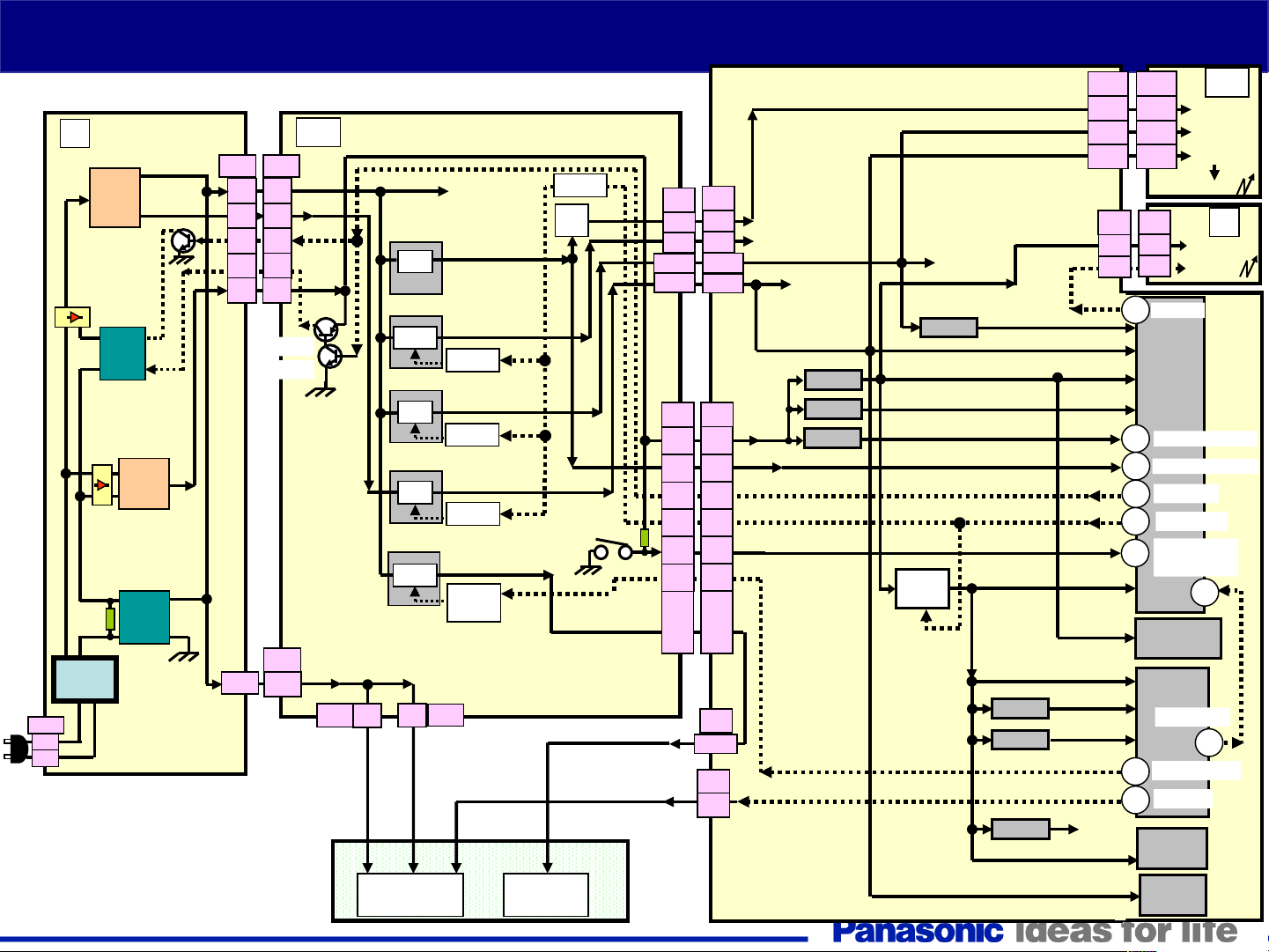
4-3-1. AP Board Regulator Circuit
15V
Q7208
Q7214
DC-DC ON/OFF Control
Q7212
Q7303
Q7301
Q7450
IC7205
5V
IC7218
18V
IC7210
9V
IC7209
9V
(*)
MIX
10V
MAIN 5V
24V
24V
SOUND 18V
MAIN 9V
BT 30V
SUB 9V
AP
(*) MAIN_5V
is regulated
from 24V
in LX60L
Q7508
Q7702
Q7701
IC7212
12V
Regulator
PANEL 12V
A
PANEL_ON from FPGA
MAIN_ON from VCTP
Page 29

4-3-2. AP Board Operation <SUB ON>
10V
24V
15V
Q7208
H
L
ON
OFF
Q7214
L
Q7212
Q7303
Q7301
Q7450
IC7205
5V
IC7218
18V
IC7210
9V
IC7209
9V
(*)
ON
MIX
10V
MAIN 5V
24V
SOUND 18V
MAIN 9V
BT 30V
SUB 9V
AP
(*) MAIN_5V
is regulated
from 24V
in LX60L
OFF
Q7508
L
Q7702
Q7701
IC7212
12V
PANEL 12V
A
PANEL_ON from FPGA
MAIN_ON from VCTP
Page 30

4-3-3. AP Board Operation <MAIN ON>
10V
24V
15V
Q7208
H
L
ON
OFF
Q7214
L
ON
Q7212
H
L
Q7303
L
Q7301
Q7450
L
H
OFF
H
OFF
H
OFF
IC7205
5V
IC7218
18V
IC7210
9V
IC7209
9V
(*)
ON
ON
ON
ON
MIX
10V
MAIN 5V
24V
SOUND 18V
MAIN 9V
BT 30V
SUB 9V
AP
(*) MAIN_5V
is regulated
from 24V
in LX60L
OFF
Q7508
L
Q7702
Q7701
IC7212
12V
PANEL 12V
A
PANEL_ON from FPGA
H
MAIN_ON from VCTP
Page 31

4-3-4. AP Board Operation <PANEL 12V ON>
10V
24V
15V
Q7208
H
L
ON
OFF
Q7214
L
ON
Q7212
H
L
Q7303
L
Q7301
Q7450
L
H
OFF
H
OFF
H
OFF
IC7205
5V
IC7218
18V
IC7210
9V
IC7209
9V
(*)
ON
ON
ON
ON
MIX
10V
MAIN 5V
24V
SOUND 18V
MAIN 9V
BT 30V
SUB 9V
AP
(*) MAIN_5V
is regulated
from 24V
in LX60L
OFF
Q7508
L
ON
Q7702
H
Q7701
L
L
H
OFF
IC7212
12V
PANEL 12V
ON
A
H
PANEL_ON from FPGA
H
MAIN_ON from VCTP
Page 32

4-4. LCD Panel Interface
A- BOARD
IC4001
VCTP
KAN_PWM
KIDO_PWM
LVDS 4ch
LVDS CLK
Inverter_SOS (H:SOS)
Inverter_ON (H:ON)
165
Analog LPF
(Q1803,Q1804
166
Level Transfer
(Q1806,Q1805)
IC4004
FPGA
LVDS 4ch
LVDS CLK
Panel 12V
6
7
For Current
control
INV-PWM
A2
28
29
30
31
2
3
4
5
LCD Panel Unit
Panel
Controller
Inverter
Board
(Not Repairable,
Unit change Only)
LCD Glasses
Horizontal
Gate Driver
Vertical
Source
Driver
P
Transformer
24V
CN2
AP1
1~9
AP
11
11
12
12
A4
AP4
IC7212
Panel 12V
A5
AP5
1~4
AP7
1~4
Back
Lights
24V
24V
Page 33

5. Explanation for Protection Circuit
Page 34

5-1. Protection Trouble Cases
When detecting irregular voltage, the circuit goes to stand-by mode to prevent
damages by over-voltage or short circuit. The power LED starts blinking as below.
Blinking
Times
2
6
7
Contents
Inverter SOS
SUB_9V down
DOWN :10V, BT 30V, SOUND 18V,
PANEL 12V,
MAIN 5V, MAIN 9V
Over Voltage :
STB 3.3V,STB 1.8V
10V(*), 24V, SUB 9V,
MAIN 5V, MAIN 9V,
SOUND 18V, PANEL 12V
VCTP’s
Pin No.
No.1 L:SOS
No.160 L:SOS
FPGA’s
Check Point
(Example)
Pin No.
LCD
No.6 H:SOS
P board
AP board
A board
AP board
A board
DT board(**)
Tuner
LCD
8
LED Blink signal
c
On
FPGA SOS
e
3.0sec (interval)
No.105 H:SOS
Light
No Light
A board
(*) except LX60L
(**) LX600/60 only
Page 35

5-2. LED 2 times Blink
LED Blink : 2 times
P
MAIN
Trans
-former
Relay
CN2 AP1
1-9
CN3 AP2
1-3
AP2 A2
13 13
1-9
1-3
Inverter_SOS
Inverter SOS
LCD
2,3,6,7 1~4AP5 AP7
24V
24V
24V
Inverter
Normal ( Low)
Abnormal (Open)
A5
2
3
5
AP
AP4
8 8
A4
3.3V
Normal ( Low)
Abnormal (High)
IC4004
H
FPGA
INV_SOS6
INV_ON
7
SDA0
IC4001
VCTP
KIDO_PWM
166
101
SUB_ON
SCL0
SDA0
SCL0
A
47
48
109
110
Relay OFF
AC
Voltage
STB
Trans
-former
Relay is turned off
Standby mode
(LED Blink : 2 times)
L
Page 36

5-3. LED 6 times Blink
LED Blink : 6 times
SUB_9V down
P
AC
Voltage
MAIN
Trans
-former
Relay
STB
Trans
-former
CN3 AP2
1-3
CN3 AP2
13 13
Relay OFF
1-3
24V
IC7209
9V
SUB_9V
AP
AP422A4
A
IC4001
VCTP
L
SUB_9VSENSE
L
1
SUB_ON
101
22
8
8
Relay is turned off
Standby mode
(LED Blink : 6 times)
Page 37

5-4. LED 7 times Blink (Case1)
LED Blink : 7 times
IC1806
STB 3.3V
3.3V
IC1807
STB 1.8V
1.8V
17-19
IC7210
AP3A317-19
AP
9V
IC7205
5V
IC7209
9V
SUB 9V
MIX
D3862
D3868
MAIN9V
MAIN5V
21,22
21,22
10V
BT30V
DOWN :10V(*),BT 30V,SOUND 18V,PANEL 12V,MAIN 5V,MAIN 9V
Overvoltage : STB 3.3V,STB 1.8V
Q3862
H
ON
STB 3.3V
L
A
Q3861
ON
IC4001
D3865
D3866
H
L
ON
L
Q3860
VCTP
TV_SOS
160
(L:SOS)
SUB_ON
101
L
AP4 AP4
(*)
D7220
D7208
MAIN 5V
L
Q7210
ON
4
4
Relay is turned off
IC7218
18V
IC7212
12V
SOUND 18V
Panel 12V
D7469
D7472
H
ON
Q7211
Standby mode
(LED Blink : 7 times)
(*) except LX60L
Page 38

5-5-1. LED 7 times Blink (Case2)
LED Blink : 7 times
P
MAIN
Trans
-former
Relay
Relay
CN3 AP2
1-3
4,5
CN3 AP2
11
CN3 AP2
131113
1-3
4,5
24V
10V
Q7223
Q7224
Overvoltage : 10V(*),24V,SUB_9V,MAIN_5V,MAIN_9V,
SOUND_18V,PANEL_12V
AP
IC7209
SUB_9V
9V
IC7218
SOUND_18V
18V
IC7210
MAIN_9V
9V
IC7205 (*)
MAIN_5V
5V
AP3
17
18
19
21
22
STB_3.3V
Q3861
Q3860
A3
17
18
19
21
22
IC4001
VCTP
160
A
TV_SOS
(L:SOS)
AC
Voltage
STB
Trans
-former
CN3 AP2
12 12
SUB_ON
Q7205
ON
Q7204
ON
IC7212
12V
H
ON
PANEL_12V
STB 7V
L
H
Q7207
27V
13V 13V
15V
22V
H
18V
7.5V
(*) MAIN_5V is regulated
from 24V in LX60L
Page 39

5-5-2. LED 7 times Blink (Case2)
LED Blink : 7 times
P
MAIN
Trans
-former
CN3 AP2
1-3
4,5
1-3
4,5
OFF
Relay
Relay
CN3 AP2
11
CN3 AP2
131113
24V
10V
Q7223
OFF
H
OFF
Q7224
Overvoltage : 10V(*),24V,SUB_9V,MAIN_5V,MAIN_9V,
SOUND_18V,PANEL_12V
AP
STB_3.3V
IC7209
Q3861
Q3860
L
SUB_9V
9V
IC7218
SOUND_18V
18V
IC7210
MAIN_9V
9V
IC7205 (*)
MAIN_5V
5V
AP3
17
18
19
21
22
A3
17
18
19
21
22
IC4001
VCTP
TV_SOS
160
(L:SOS)
A
AC
Voltage
STB
Trans
-former
CN3 AP2
12 12
SUB_ON
Q7205
ON
Q7204
ON
IC7212
12V
H
ON
PANEL_12V
STB 7V
L
H
Q7207
27V
13V 13V
15V
22V
H
18V
7.5V
(*) MAIN_5V is regulated
from 24V in LX60L
Page 40

5-5-3. LED 7 times Blink (Case2)
LED Blink : 7 times
P
MAIN
Trans
-former
CN3 AP2
1-3
4,5
1-3
4,5
OFF
Relay
Relay
CN3 AP2
11
CN3 AP2
131113
24V
10V
Q7223
OFF
H
OFF
Q7224
Overvoltage : 10V(*),24V,SUB_9V,MAIN_5V,MAIN_9V,
SOUND_18V,PANEL_12V
AP
STB_3.3V
IC7209
H
Q3861
ON
ON
Q3860
L
SUB_9V
9V
IC7218
SOUND_18V
18V
IC7210
MAIN_9V
9V
IC7205 (*)
MAIN_5V
5V
AP3
17
18
19
21
22
A3
17
18
19
21
22
IC4001
VCTP
L
TV_SOS
160
(L:SOS)
A
AC
Voltage
STB
Trans
-former
CN3 AP2
12 12
SUB_ON
Q7205
ON
Q7204
ON
IC7212
12V
H
ON
PANEL_12V
STB 7V
L
H
Q7207
27V
13V 13V
15V
22V
H
7.5V
18V
Standby mode
(LED Blink : 7 times)
(*) MAIN_5V is regulated
from 24V in LX60L
Page 41

5-6. LED 8 times Blink
LED Blink : 8 times
P
AC
Voltage
MAIN
Trans
-former
Relay
STB
Trans
-former
Relay OFF
CN3 AP2
13 13
12 12
AP
STB 7V
AP4 A4
8 8
3 3
IC1806
Q1801
Q1802
STB3.3V
IC1805
IC1804
MAIN3.3V
MAIN 2.5V
MAIN 1.5V
L
IC4004
FPGA
FPGA_OK
IC4001
VCTP
MAIN_ON
102
SUB_ON
101
A
97
H
105
Relay is turned off
Standby mode
(LED Blink : 8 times)
Page 42

6. Troubleshooting
Page 43

6-1. Signal Trouble Cases
We can classify the signal problem into three by checking whether Picture or Sound
is abnormal.
It is important to check whether both picture trouble and sound trouble occur,
because we can judge the cause is panel or video processor or sound processor.
Picture NG and Sound OK
1)
Picture OK and Sound NG
2)
Picture NG and Sound NG
3)
Page 44

6-2-1. Picture NG and Sound OK (LX600/LX60 except 23LX60)
No
ALL Input Source
Picture NG ?
Only AV Terminal
Picture NG
A Board
Yes
Analog TV
Picture NG
Only Digital
TV Picture NG
Only HDMI
Input Picture NG
AV Terminal
Picture OK?
DT Board
DT Board
A Board
Yes
No
LX600 only
A
DT
TUNER
A Board
ATSC
LSI
HDMI1
HDMI2
PEAKS
LITE
HDMI
I/F
Y/C
Included OSD
VCTP
Digital
OSD
No picture but
OSD is displayed ?
Yes
A Board
No
LCD Panel or A board
AV1
AV2
COMPONENT
Monitor Out
AV3
G
VIDEO
SWITCH
OSD
VIDEO
PROCESSOR
LVDS
FPGA
LCD
Panel
Page 45

6-2-2. Picture NG and Sound OK (32/26LX60C/L)
No
ALL Input Source
Picture NG ?
Only AV Terminal
Picture NG
A Board
Yes
No picture but
OSD is displayed ?
Yes
A Board
No
Analog TV
Picture NG
Only HDMI
Input Picture NG
LCD Panel or A board
AV Terminal
Picture OK?
Yes
Tuner
A Board
No
A
TUNER
AV1
AV2
COMPONENT
Monitor Out
G
A Board
AV3
except 23LX60
HDMI1
HDMI
I/F
VCTP
VIDEO
SWITCH
Digital
OSD
OSD
VIDEO
PROCESSOR
LVDS
FPGA
LCD
Panel
Page 46

6-2-3. Picture NG and Sound OK (23LX60)
No
ALL Input Source
Picture NG ?
Only AV Terminal
Picture NG
A Board
Yes
No picture but
OSD is displayed ?
Yes
A Board
No
Analog TV
Picture NG
Only HDMI
Input Picture NG
LCD Panel or A board
AV Terminal
Picture OK?
Yes
Tuner
A Board
No
A
TUNER
AV1
AV2
COMPONENT
Monitor Out
G
A Board
AV3
except 23LX60
HDMI1
HDMI
I/F
VCTP
VIDEO
SWITCH
Digital
OSD
OSD
VIDEO
PROCESSOR
LVDS
FPGA
LCD
Panel
Page 47

6-3-1. Picture OK and Sound NG (LX600/60 except 23LX60)
ALL Input Source
Sound NG ?
Yes
Headphone or
Audio OUT
Sound NG ?
No
Only AV Terminal
Sound NG
Analog TV
Sound NG
Digital TV
Sound NG
Only HDMI Input
Sound NG
No
A Board (Audio AMP)
or Speaker
A Board
AV Terminal
Sound OK?
Yes
DT Board
AV Terminal
Sound OK?
Yes
DT Board
A Board
No
No
A Board
A Board
LX600 only
A
DT
TUNER
Digital
Audio OUT
AV1
AV2
DVI (Analog)
Audio In
Monitor Out
ATSC
LSI
HDMI1
HDMI2
PEAKS
LITE
Audio
DAC
HDMI I/F
Audio
SW
Audio
ADC
L/R
L/R
L/R
L/R
L/R
L/R
VCTP
MSP
SW
AUDIO
SWITCH
L/R
L/R
L/R
Audio
AMP
HP
AMP
L
R
L/R
Yes
A Board
G
Headphone
AV3
L/R
Page 48

6-3-2. Picture OK and Sound NG (32/26LX60C/L)
ALL Input Source
Sound NG ?
Headphone or
Audio OUT
Sound NG ?
No
Only AV Terminal
Sound NG
Analog TV
Sound NG
Only HDMI Input
Sound NG
No
A Board (Audio AMP)
or Speaker
A Board
AV Terminal
Sound OK?
Yes
DT Board
A Board
No
A Board
A
TUNER
AV1
AV2
DVI (Analog)
Audio In
Monitor Out
HDMI1
IC2202
HDMI I/F
L/R
L/R
L/R
L/R
L/R
L/R
VCTP
MSP
SW
AUDIO
SWITCH
L/R
L/R
L/R
L/R
L/R
Audio
AMP
HP
AMP
L
R
L/R
Yes
A Board
G
Headphone
AV3
L/R
except 23LX60
Page 49

6-3-3. Picture OK and Sound NG (23LX60)
ALL Input Source
Sound NG ?
Headphone or
Audio OUT
Sound NG ?
No
Only AV Terminal
Sound NG
Analog TV
Sound NG
Only HDMI Input
Sound NG
No
A Board (Audio AMP)
or Speaker
A Board
AV Terminal
Sound OK?
Yes
DT Board
A Board
No
A Board
A
TUNER
AV1
AV2
DVI (Analog)
Audio In
Monitor Out
HDMI1
IC2202
HDMI I/F
L/R
L/R
L/R
L/R
L/R
L/R
VCTP
MSP
SW
AUDIO
SWITCH
L/R
L/R
L/R
L/R
L/R
Audio
AMP
HP
AMP
L
R
L/R
Yes
A Board
G
Headphone
AV3
L/R
except 23LX60
Page 50

6-4-1. Picture NG and Sound NG (LX600/60 except 23LX60)
LX600 only
Input Source
check
Analog TV
Picture NG
Sound NG
AV Terminal
Picture NG
Sound NG
HDMI Input
Picture NG
Sound NG
Digital TV
Picture NG
Sound NG
AV Terminal
Picture &
Sound OK?
Yes
DT Board
A Board
A Board
AV Terminal
Picture &
Sound OK?
Yes
DT Board
No
A Board
No
A Board
A
DT
TUNER
AV1
AV2
COMPONENT
Monitor Out
AV3
G
LX600 only
A
DT
TUNER
Digital
Audio OUT
AV1
AV2
DVI (Analog)
Audio In
Monitor Out
ATSC
LSI
ATSC
LSI
HDMI1
HDMI2
PEAKS
HDMI1
HDMI2
PEAKS
LITE
LITE
HDMI
I/F
Audio
DAC
Y/C
HDMI I/F
Audio
SW
Audio
ADC
L/R
L/R
L/R
L/R
L/R
Included OSD
VCTP
VIDEO
SWITCH
VCTP
MSP
SW
L/R
AUDIO
SWITCH
Digital
OSD
OSD
VIDEO
PROCESSOR
LVDS
L/R
L/R
L/R
FPGA
Audio
AMP
HP
AMP
LCD
Panel
L
R
L/R
G
Headphone
AV3
L/R
Page 51

6-4-2. Picture NG and Sound NG (32/26LX60C/L)
Input Source
check
Analog TV
Picture NG
Sound NG
AV Terminal
Picture NG
Sound NG
HDMI Input
Picture NG
Sound NG
AV Terminal
Picture &
Sound OK?
Yes
Tuner
A Board
A Board
No
A Board
A
TUNER
AV1
AV2
COMPONENT
Monitor Out
AV3
G
except 23LX60
A
TUNER
AV1
AV2
DVI (Analog)
Audio In
Monitor Out
HDMI1
HDMI1
IC2202
HDMI
I/F
HDMI I/F
L/R
L/R
L/R
L/R
L/R
VCTP
VIDEO
SWITCH
MSP
SW
AUDIO
SWITCH
Digital
OSD
OSD
VIDEO
PROCESSOR
LVDS
L/R
L/R
L/R
L/R
L/R
Audio
AMP
HP
AMP
FPGA
L/R
LCD
Panel
L
R
G
Headphone
AV3
L/R
except 23LX60
Page 52

6-4-3. Picture NG and Sound NG (23LX60)
Input Source
check
Analog TV
Picture NG
Sound NG
AV Terminal
Picture NG
Sound NG
HDMI Input
Picture NG
Sound NG
AV Terminal
Picture &
Sound OK?
Yes
Tuner
A Board
A Board
No
A Board
A
TUNER
AV1
AV2
COMPONENT
Monitor Out
AV3
G
except 23LX60
A
TUNER
AV1
AV2
DVI (Analog)
Audio In
Monitor Out
HDMI1
HDMI1
IC2202
HDMI
I/F
HDMI I/F
L/R
L/R
L/R
L/R
L/R
VCTP
VIDEO
SWITCH
MSP
SW
AUDIO
SWITCH
Digital
OSD
OSD
VIDEO
PROCESSOR
LVDS
L/R
L/R
L/R
L/R
L/R
Audio
AMP
HP
AMP
FPGA
L/R
LCD
Panel
L
R
G
Headphone
AV3
L/R
except 23LX60
Page 53

6-5. Power LED No Light
Power LED Status
No Light
Relay doesn’t turn ON by Power SW ON and Remote Power ON
1
AC output
between 1 and 3 pin
of CN1 ?
2
When AC Plug IN,
STB 7V output
at AP2’s 12 pin ?
Yes
A Board
Yes
No(STB7V NG)
P
No
AC power code NG or Power Source NG
MAIN
Defective Board
P, AP, A Board
Disconnect AC Cord.
3 4
Disconnect A4.
A4’s 3 pin Short
with GND?
Yes
A Board
AP
Trans
-former
Power SW
Relay
Relay
CN3 AP2
13 13
STB
12 12
Trans
-former
Relay
R
Disconnect AC Cord.
No
Disconnect CN3.
AP2’s 12 pin Short
with GND?
AP Board
AP4 A4
7 7
8 8
3 3
342
Yes
A
STB 7V
No
IC1806
IC1807
IC1803
P Board
STB3.3V
STB1.8V
RESET
Note :
How to stop power supply completely is
disconnecting AC cord,
not turning OFF the power SW.
V
STB 3.3V
REMOTE
IC4001
VCTP
V1
A1
44
3
55
KEY_SCAN
161
POW
SUB_ON
101
1
CN1
3
1
Line
Filter
Page 54

6-6. LED 2 times Blink
Trouble Mode Defective Board
Inverter SOS LCD module, P, A Board
Power SW ON.
1
24V output
at CN2’s 1~9 pin OK
before Shutdown ?
Yes
2
Power SW ON.
INV_ON output
at A5’s 3 pin
before Shutdown ?
Yes
Power SW ON.
3
KIDO_PWM output
at A5’s 5pin
before Shutdown ?
No
P Board
No
A Board
No
A Board
Inverter SOS
LCD
24V
Normal ( Low)
Abnormal (Open)
Inverter
Normal ( Low)
Abnormal (High)
3.3V
IC4004
A5
2
2
3
5
3
FPGA
INV_SOS
6
7
INV_ON
SCL0
A
47
Yes
LCD Panel
P
AC
Voltage
MAIN
Trans
-former
Relay
STB
Trans
-former
1
CN2 AP1
1-9
1-9
CN3 AP2
1-3
1-3
AP2 A2
13 13
Relay OFF
24V
24V
2,3,6,7 1~4AP5 AP7
AP
AP4
8
A4
8
L
SDA0
IC4001
VCTP
KIDO_PWM
166
SDA0
SCL0
101
SUB_ON
48
109
110
Page 55

6-7. LED 6 times Blink
Trouble Mode Defective Board
SUB 9V down AP, P Board
1 2
Power SW ON.
SUB 9V output
at AP4’s 22 pin OK
before Shutdown ?
No
Disconnect A4.
A4’s 22 pin Short
with GND ?
No
Note :
How to stop power supply completely is disconnecting AC cord,
not turning OFF the power SW.
AP Board
Yes
A Board
P
MAIN
Trans
-former
Relay
A Board
CN3 AP2
1-3
1-3
CN3 AP2
13 13
Relay OFF
Yes
24V
IC7209
9V
SUB_9V
AP
AP422A4
1
8
22
8
A
IC4001
VCTP
L
SUB_9VSENSE
1
2
SUB_ON
101
L
AC
Voltage
STB
Trans
-former
Page 56

6-8-1. LED 7 times Blink
Trouble Mode Defective Board
Case1) DOWN :10V,BT 30V, SOUND 18V, PANEL 12V, MAIN 5V, MAIN 9V
Over Voltage : STB 3.3V, STB 1.8V
Case2) Over Voltage : 10V, 24V, SUB 9V, MAIN 5V, MAIN 9V, SOUND 18V, PANEL 12V
1
Q7207’s base
No
(case1)
voltage is high
before shutdown ?
Yes
(case2)
No
2
Power SW on.
24V output
(24V or
10V over)
at AP2’s 1~3 pin or
10V output
at AP2’s 4~5 pin
before shutdown ?
Yes
(The other
volts over)
AP Board
P Board
Note :
"Power comes up" means shutdown doesn't occur.
3
Disconnect A2.
After Power SW ON,
Power comes up ?
Yes
LCD
Panel
P
24V
Trans
10V
SUB
ON
Relay
RELAY
STB
Trans
4
CN3
1-3
4,5
13 13
11
12 12
No
4
Disconnect AC cord.
Disconnect CN3.
CN3’s 4 or 5 pin
Short with GND ?
P Board
AP
AP2
2
1-3
4,5
11
Q7223
Q7224
1
Yes
24V
IC7209
9V
IC7218
18V
IC7210
9V
IC7205
5V
IC7212
12V
Q7204-7
5 6
Disconnect AC cord.
Disconnect A3.
No
AP3’s 2 or 3 or 7 or 17~19
or 21~22 pin
Short with GND ?
AP Board
Q7210
Q7211
MIX
10V
SUB_9V
PANEL_12V
Yes
LCD
AP3
7
2,3
17-19
21,22
AP4
1
22
3
8
11
12
P,AP,A,DT Board,
Tuner, LCD
Remove DT Board.
No
After Power SW ON,
Power comes up ?
DT Board
A3
7
2,3
17-19
21,22
Q3861
Q3860
A4
1
22
3
8
11
12
A2
STB7V
A
BT_30V
SOUND_18V
MAIN 9V
MAIN 5V
IC4002
Q3862
SUB
9V
IC1806
IC1807
IC4001
(VCTP)
160
101
5
3
Yes
MAIN 8V
TV_SOS
SUB_ON
6
DT12
A12
51-53
51-53
54,57
54,57
STB
3.3V
STB
1.8V
SOS:L
No
88
A Board
DT
BT_30V
MAIN_9V
MAIN_5V
Page 57

6-8-2. LED 7 times Blink (LX60C/L)
Trouble Mode Defective Board
Case1) DOWN :BT 30V, SOUND 18V, PANEL 12V, MAIN 5V, MAIN 9V
Over Voltage : STB 3.3V, STB 1.8V
Case2) Over Voltage : 24V, SUB 9V, MAIN 5V, MAIN 9V, SOUND 18V, PANEL 12V
1
Q7207’s base
voltage is high
before shutdown ?
Yes
(case2)
No
(case1)
3
Disconnect A2.
After Power SW ON,
Power comes up ?
Yes
LCD
Panel
No
Disconnect AC cord.
4
Disconnect A3.
AP3’s 2 or 3 or 7 or 17~19
or 21~22 pin
Short with GND ?
Yes
AP Board
5
No
Remove Tuner.
After Power SW ON,
Power comes up ?
AP
P
2
Power SW on.
No
(24V
over)
24V output
at AP2’s 1~5 pin or
before shutdown ?
Yes
(The other
volts over)
AP Board
P Board
Note :
"Power comes up" means shutdown doesn't occur.
Trans
SUB
ON
Relay
RELAY
STB
Trans
24V
CN3
1-3
4,5
13 13
11
12 12
AP2
1-3
4,5
11
Q7223
Q7224
2
1
24V
IC7209
9V
IC7218
18V
IC7210
9V
IC7205
5V
IC7212
12V
Q7204-7
MIX
SUB_9V
Tuner
Q7210
Q7211
PANEL_12V
LCD
Yes
AP3
7
2,3
17-19
21,22
AP4
1
22
3
8
11
12
P, AP, A board,
Tuner, LCD
No
A Board
A3
7
2,3
17-19
21,22
Q3861
Q3860
A4
1
22
3
8
11
12
A2
STB7V
A
BT_30V
SOUND_18V
IC4002
Q3862
SUB
9V
160
101
4
3
MAIN 9V
MAIN 5V
IC1806
IC1807
IC4001
(VCTP)
TV_SOS
SUB_ON
5
TUNER
BT_30V
MAIN_5V
MAIN 8V
STB
3.3V
STB
1.8V
SOS:L
Page 58

6-9. LED 8 times Blink
Trouble Mode Defective Board
P
AC
Voltage
FPGA SOS
MAIN
Trans
-former
Relay OFF
Relay
STB
Trans
-former
CN3 AP2
13 13
12 12
A Board (*)
(*) Cause
e.g. IC4004 (FPGA) or MAIN 3.3V/2.5V/1.5V line abnormal
AP
MAIN3.3V
MAIN 2.5V
MAIN 1.5V
102
101
L
FPGA_OK
STB 7V
AP4 A4
8 8
3 3
IC1806
Q1801
Q1802
IC1805
IC1804
STB3.3V
IC4004
FPGA
IC4001
VCTP
MAIN_ON
SUB_ON
A
97
H
105
Page 59

<Hands on for LCD>
Page 60

1. Typical Trouble Example
Page 61

1-1. Picture Trouble Example
<Photo of Symptom>
Model : All Models
Symptom : Horizontal Line
Result : LCD Panel
Model : All Models
Symptom : Wide Vertical Line
Result : LCD Panel
Model : All Models
Symptom : Horizontal Line
Result : LCD Panel
Model : All Models
Symptom : Vertical Line
Result : LCD Panel
Model : All Models
Symptom : Vertical Line
Result : LCD Panel
Model : All Models
Symptom : Irregular Color
Result : LCD Panel
Model : All Models
Symptom : Irregular Color
Result : LCD Panel
Model : All Models
Symptom : Abnormal Picture (Lower)
Result : LCD Panel
Model : All Models
Symptom : Abnormal Picture (Right Half)
Result : LCD Panel
Page 62

1-2. Picture Trouble Example
<Photo of Symptom>
Model : All Models
Symptom : Vertical Line
Result : DG Board
Model : All Models
Symptom : Vertical Noise (Red)
Result : DG Board
Model : All Models
Symptom : OSD NG
Result : DG Board
Model : All Models
Symptom : Abnormal Color
Result : DG Board
Model : All Models
Symptom : Picture NG (Sub Window)
Result : DG Board
Model : Japan Models
Symptom : Sub Window Picture NG (EPG)
Result : DG Board
Model : All Models
Symptom : Vertical Line
Result : LCD Panel
Model : All Models
Symptom : Light Color
Result : LCD Panel
Page 63

2. The Idea of Diagnosis for LCD
Page 64

2-1. Diagnosis by Jig
<Purpose>
In case of LCD, the picture problem is mainly caused by LCD panel or DG(A) board defective.
This Jig is able to diagnose these defective parts.
<Model>
TC-32/26LX600 (for USA, Canada)
TC-32/26LX60 (for USA), TC-32/26LX60C (for Canada)
TC-23LX60 (for USA, Canada)
TC-32/26LE60 (derivartive model), TC-26/23LX60L (for Latin)
TC-26/23LX60C (for Mexico)
<How to connect the Jig>
(Original)
LCD panel
DG(A) Board
LVDS cable
T-con board
(on the panel)
<Jig>
Connecting Board
No : TZSC07063
Cable
No : TZSC09035
( Include Connecting board, Cable)
<Diagnosis>
If the test pattern is normally displayed,
defective parts is DG board mainly.
If the test pattern is abnormally displayed,
defective part is LCD panel side.
(After connecting Jig)
LCD panel
DG(A) Board
Jig
(Connecting board, Cable)
T-con board
(on the panel)
LVDS cable
<Test Pattern>
The test pattern is automatically displayed in turn
as follows by connecting Jig.
Red
Black
Green Blue
White
Page 65

3. Introduction of Jig
Page 66

3-1-1. Extension Cable (TC-32/26LX600/60)
Panel
G
SP
AP
A
DT
Tcon
To A2
Inverter Board
Panel
P
AP
AP3 AP4
AP5
P
G
G4
SP
CN2
V
AP3-A3,
AP4-A4
( TZSA09014
)
SP
V1
V
SP
Panel unit
CN2-AP5,A5
( TZSC07049)
G4-A6
( TZSC07051
)
SP(R,L)-A7
( TZSC09029
)
A5
A6
A7
A1
A board
A3 A4
A12
A2
( TZSC07048
V1-A1
)
DT12
DT board
Tcon-A2
( TZSA09012
)
DT12-A12
( TZSC09012
)
Page 67

3-1-2. Extension Cable (TC-32/26LX60C/L)
Panel
G
SP
AP
A
Tcon
To A2
Inverter Board
Panel
P
AP
AP3 AP4
AP5
P
G
G4
SP
CN2
V
AP3-A3,
AP4-A4
( TZSA09014
)
SP
V1
V
SP
Panel unit
CN2-AP5,A5
( TZSC07049)
G4-A6
( TZSC07051
)
SP(R,L)-A7
( TZSC09029
)
A5
A6
A7
A1
A board
A3 A4
Tcon-A2
( TZSA09012
)
A2
V1-A1
( TZSC07048
)
Page 68

3-1-3. Extension Cable (TC-23LX60)
Panel
A
AP
P
Panel
AP
AP3 AP4
P
SP
Inverter Board
Panel unit
Tcon
SP
V
CN2-AP5,A5
( TZSC07050)
( TZSC07052
K
K1-A6
)
SP
A7
A6
A5
A1
A3 A4
A2
V
V1
SP
AP3-A3,
AP4-A4
( TZSA09014
)
K1
K
Tcon-A2
( TZSA09012
)
SP(R,L)-A7
( TZSC09029
)
A board
V1-A1
( TZSC07048
)
Page 69

3-2-1. Extension Cable Connection (USA)
<Back Side View>
<Front Side View>
e.g. TC-32LX60
A Board
DT Board
Page 70

3-2-2. Extension Cable Connection (Canada/ Latin)
<Back Side View>
e.g. TC-32LX60C
<Front Side View>
A Board
Page 71

3-2-3. Extension Cable Connection (Canada)
<Back Side View>
e.g. TC-23LX60C
<Front Side View>
A Board
Page 72

3-3. List of Extension Cable
Please refer to the another sheet
Page 73

End of Presentation
End of Presentation
Thank you very much for attending seminar
Thank you very much for attending seminar
Page 74

Appendix
Page 75

1: Service Mode (LX600/LX60)
How to enter Service Mode (No change from LX50)
While pressing [VOLUME - ] button of the main unit,
press [RECALL] button of the remote control three times in a row (within 2 seconds).
Adjustment functions (change from LX50)
MAIN_ADJ
PCT_ADJ
MTS_ADJ
LX50 (Current)
PICTURE1
B-Y
R-Y
COLOR
TINT
BRIGHT
BACK-L
B-Y-G
R-Y-A
OPT00OPTION
EEPROM COPY
CODERM_SET
MTSIN
SEPAL
SEPAH
RemarksSub ItemMain Item
Sub-Color
Sub-Tint
Sub-BRT
Sub-BACKLIGHT
B-Y Gain
R-Y Angle
ALL or ADJ
Remote Code
“MAIN ADJ”
Delete
“WB ADJ”
Add
“RM SET”
“MTS”
Delete
“STB_CAS”
Add
PCT_ADJ
LX600 (New)
COLOR
TINT
BACK-L
B-Y-G
R-Y-A
R-GAINWB_ADJ
G-GAIN
B-GAIN
R-CENT
G-CENT
B-CENT
OPT00OPTION
BOOT ROM
EEPROM COPY
CEC_CHK
Hard TestSTB_CAS(*)
SD Download
Err log
RemarksSub ItemMain Item
Sub-Color
Sub-Tint
Sub-BACKLIGHT
B-Y Gain
R-Y Angle
WHITE 100%(ADJ)
WHITE 100%(ADJ)
WHITE 100%(ADJ)
WHITE 50%(ADJ)
WHITE 50%(ADJ)
WHITE 50%(ADJ)
ROM or SD
ALL or ADJ or FIX
(*) Note Pressing “OK” button is necessary to access Sub item.
Page 76

2: Service Mode (LX60C/L)
How to enter Service Mode (No change from LX50)
While pressing [VOLUME - ] button of the main unit,
press [RECALL] button of the remote control three times in a row (within 2 seconds).
Adjustment functions (change from LX50)
MAIN_ADJ
PCT_ADJ
MTS_ADJ
LX50 (Current)
PICTURE1
B-Y
R-Y
COLOR
TINT
BRIGHT
BACK-L
B-Y-G
R-Y-A
OPT00OPTION
EEPROM COPY
CODERM_SET
MTSIN
SEPAL
SEPAH
RemarksSub ItemMain Item
Sub-Color
Sub-Tint
Sub-BRT
Sub-BACKLIGHT
B-Y Gain
R-Y Angle
ALL or ADJ
Remote Code
“MAIN ADJ”
Delete
“WB ADJ”
Add
“RM SET”
Delete
PCT_ADJ
LX60 (New)
COLOR
TINT
BACK-L
B-Y-G
R-Y-A
R-GAINWB_ADJ
G-GAIN
B-GAIN
R-CENT
G-CENT
B-CENT
OPT00OPTION
EEP COPY
MTSINMTS_ADJ
SEPAL
SEPAH
RemarksSub ItemMain Item
Sub-Color
Sub-Tint
Sub-BACKLIGHT
B-Y Gain
R-Y Angle
WHITE 100%(ADJ)
WHITE 100%(ADJ)
WHITE 100%(ADJ)
WHITE 50%(ADJ)
WHITE 50%(ADJ)
WHITE 50%(ADJ)
ALL or ADJ or FIX
WB-ADJ is necessary when LCD panel is exchanged.
MTS-ADJ is necessary when tuner or Multi-sound-IC(IC2202) is exchanged.
Mainly, OPTION are not necessary to adjust and PCT_ADJ is done if necessary.
Page 77

3: Self Check
How to enter Self Check (No change from LX50)
While pressing [VOLUME - ] button of the main unit,
press [SLEEP] button of the remote control simultaneously.
Screen Display example
LX600/LX60 only
SELF CHECK 03700-03700
UV OK DT1 OK DT2 OK
AVSWA OK FPGA OK HDMI OK
MEM OK VCTP OK CEC OK
SOS : 2 7
Table 1 Meaning of items
BoardDescriptionRef. No.Display
DT BoardTV TunerTH8200UV
DT BoardPEAKS_Lite(*1)IC8240DT1
DT BoardPEAKS_Lite(*2)IC8240DT2
A BoardAudio SWIC2602AVSWA
A BoardLCD DriverIC4004FPGA
A BoardHDMI ReceiverIC5004HDMI
A BoardEEPROMIC1102MEM
except LX60L
Software Version – EEPROM data Version
Basically, “OK” in green or “NG” in red is displayed.
But, NG of DT1, DT2, and HDMI are displayed
in hexadecimal number and NG of CEC is
displayed as ‘---’ .
SOS History
Note:
*1 DT1’s NG means the communication error
between VCTP and Peaks_Lite.
*2 DT2’s NG means the Peaks_Lite can’t communicate
with the peripheral devices such as EEPROM,
ATSC LSI (FRONT END LSI) and NTSC ENCORDER
through IIC bus line.
A BoardDigital ProcessorIC4001VCTP
A BoardCEC ControlIC4001CEC
Page 78

4: SOS History
We can confirm the record of Power SOS by Self-check.
This information is useful for service, if TV set sometimes shuts down
by power supply trouble.
Screen Display example LX600/LX60
SELF CHECK 03700-03700
UV OK DT1 OK DT2 OK
AVSWA OK FPGA OK HDMI OK
MEM OK VCTP OK CEC OK
SOS : 2 7
Note:
*This data is only displayed if TV set sometimes shuts down by power supply trouble
during the time from the former self check to the next self check.
*This data shows all kinds of LED blink that occurred during the time from the former self check
to the next self check.
*This data is cleared after self check.
In case of LED Blink 2 and 7 times
 Loading...