

Page 1
LX600 LCD TV Technical Information
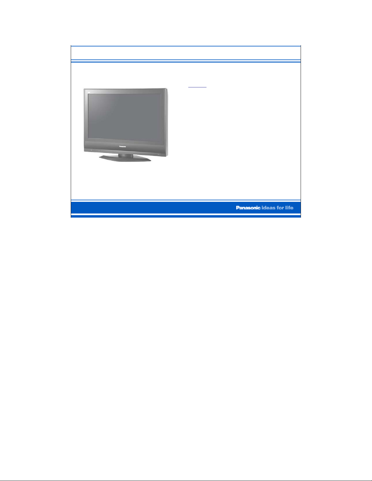
TC-32LX600
Outline
Features
Overall Block Diagram
A Board Main Layout
Power On Sequence
Protection Shutdown
Troubleshooting
Adjustments
1
Page 2
Features
Model
Display Capability
Aspect Ratio 16:9 (Widescreen) 16:9 (Widescreen)
Aspect Control Normal, Zoom, Full, and
Resolution (Number of
Pixels)
Contrast Ratio Up to 3000:1 Up to 3000:1
Brightness (Panel, cd/m2) 500 500
Integrated ATSC Tuner Yes Yes
HDMI-HDCP Interface 1 2
Composite Video Input 3 3
S-Video Inputs 2 2
Component Video Input 1 1
Monitor Output 1 1
Headphone Jack Yes Yes
TC-LX60
480p/720p/1080i 480p/720p/1080i
Just
1,049,088 (1366x768)
pixels
TC-LX600
Normal, Zoom, Full, and
Just
1,049,088 (1366x768)
pixels
2
Page 3
Overall Block Diagram
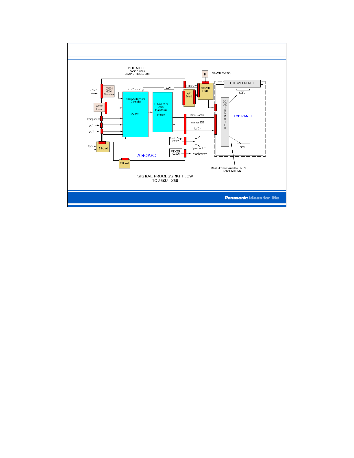
The TC-26/32LX60 and 600 series LCD Direct View TVs differ from previous
models in that all signal processing is accomplished on the A board. The
video processing function that had been previously accomplished by the DG
board is now performed on the A Board by IC4002. This IC serves as the
Main micro and Video /Audio Panel controller. IC4004 is a Field
Programmable Gate array that is responsible for the pixel conversion and
addressing of the Active Matrix display within the LCD Panel. This IC also
contains the low voltage differential signaling (LVDS) transmitter used for the
conversion of the 8-bit RGB video into a differential RGB output signal. The
LVDS receiver on the LCD panel converts the differential RGB output signal
from the A board into an 8-bit RGB signal that is output to the LCD Panel.
3
Page 4
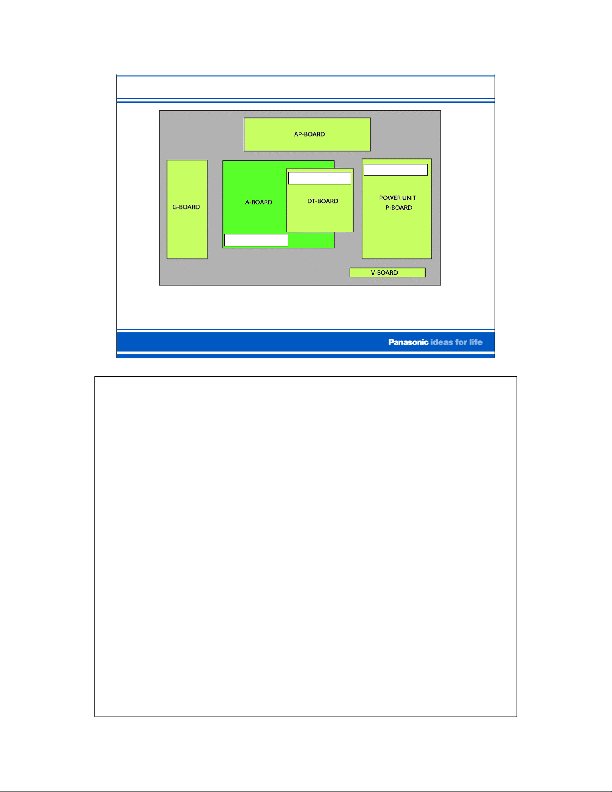
Board Layout
Non - Serviceable
Non - Serviceable
Non - Serviceable
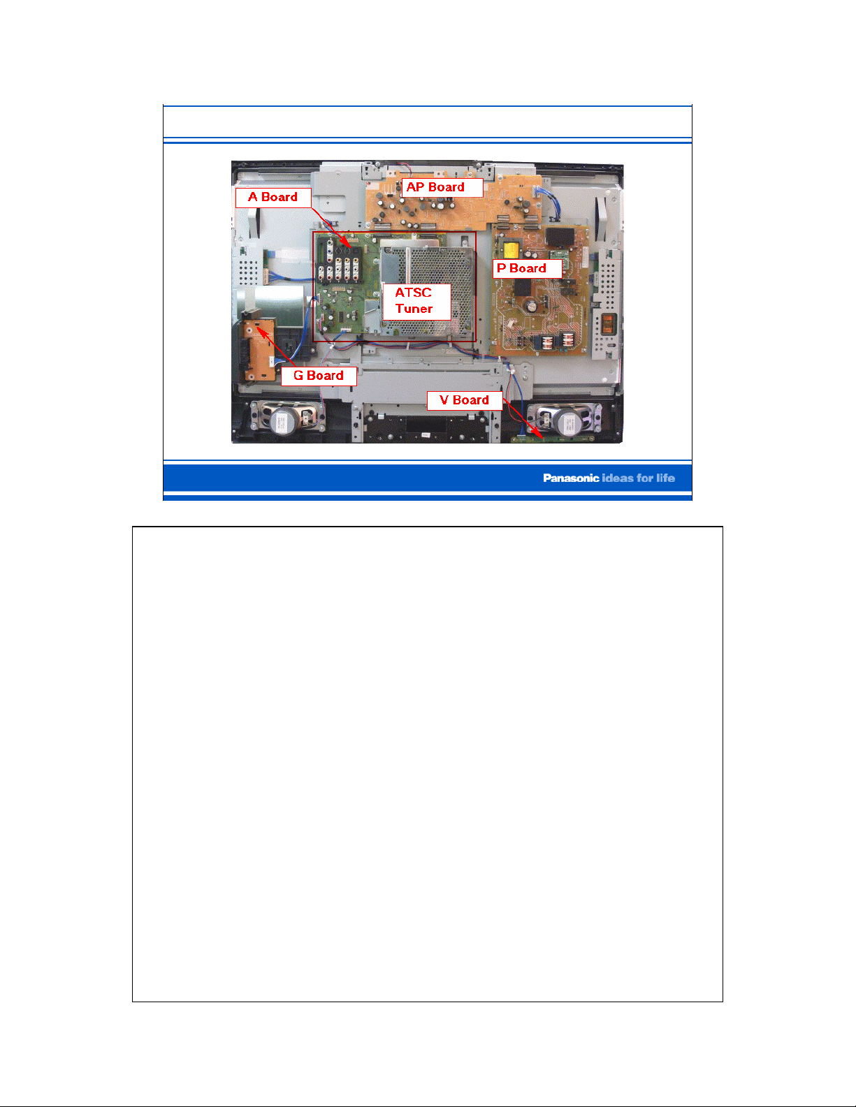
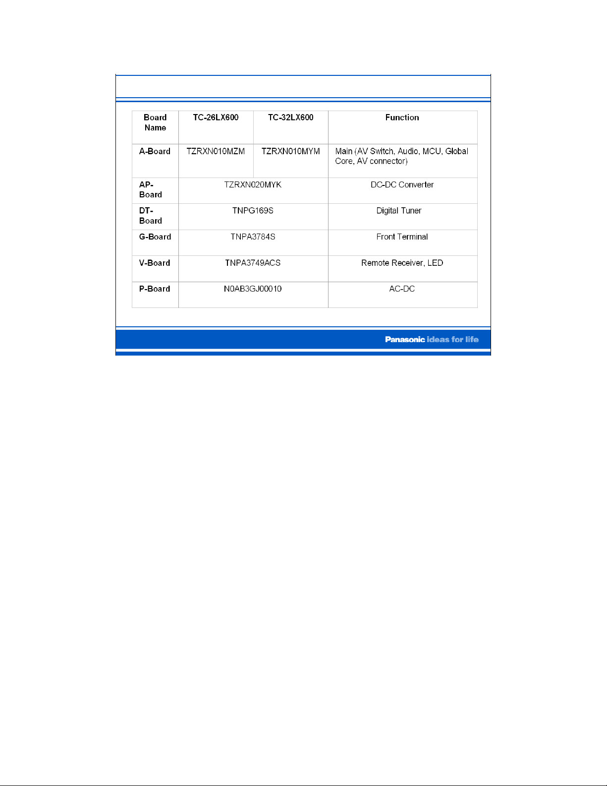
This is the board layout of the TC-LX600 LCD Television. The P board, DT
board, and A board are non serviceable. The G board, AP board, and V
board are serviceable.
4
Page 5
Board Layout Pictorial
P Board – The Power unit is responsible for generating the Standby 7V, 10V, and
24V, which provides input to some of the regulators on the AP Board. It also
generates the switched 24V inverter voltage.
AP Board – Comprised of all secondary voltages which include the Main 9V,
SUB5V, Sound 20V, Panel 12V, Standby 3.3V.
A Board – Comprised of all AV inputs and the HDMI interface with the exception
of one AV jack which is located on the G board. All audio and video processing is
performed on this board.
G Board – Contains an additional AV connector and the Headphone Jack.
ATSC tuner – The Digital Tuner plugs into a connection on the A board.
V Board - Remote sensor and Power LED.
5
Page 6
Board Description
6
Page 7
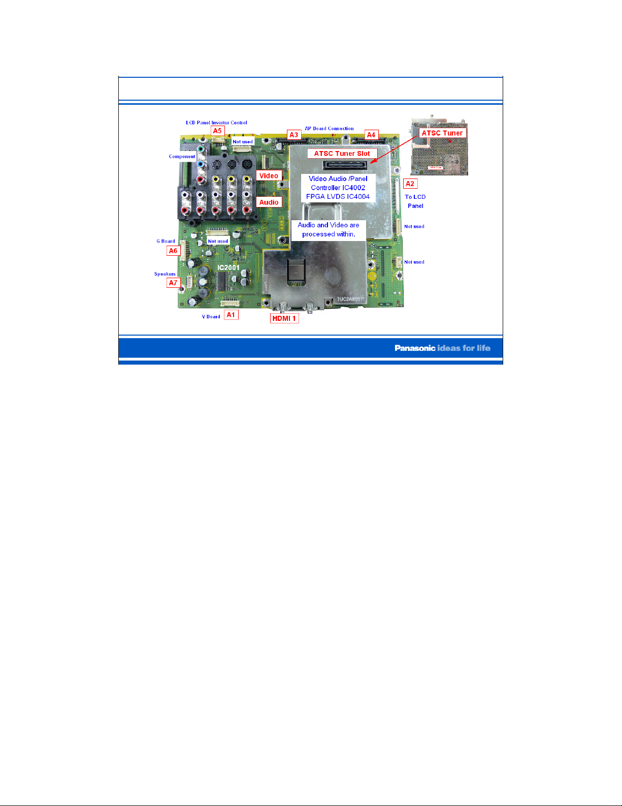
A
Board Main
The A board (Main Board) is a self contained board responsible for the
input selection, and processing of all Audio and Video input signals. All
audio and video connections with the exception of those found on the G
board reside on this board. The G board contains an additional AV Jack,
headphone jack, and front panel switches. The unit is equipped with a
single ATSC tuner which plugs directly onto the A board. The LX60
features a single HDMI interface while the LX600 offers two.
The connectors and pin outs provided in this diagram are, for the most
part, the only available access points for board level repair
troubleshooting.
7
Page 8
A
Board Video Processing
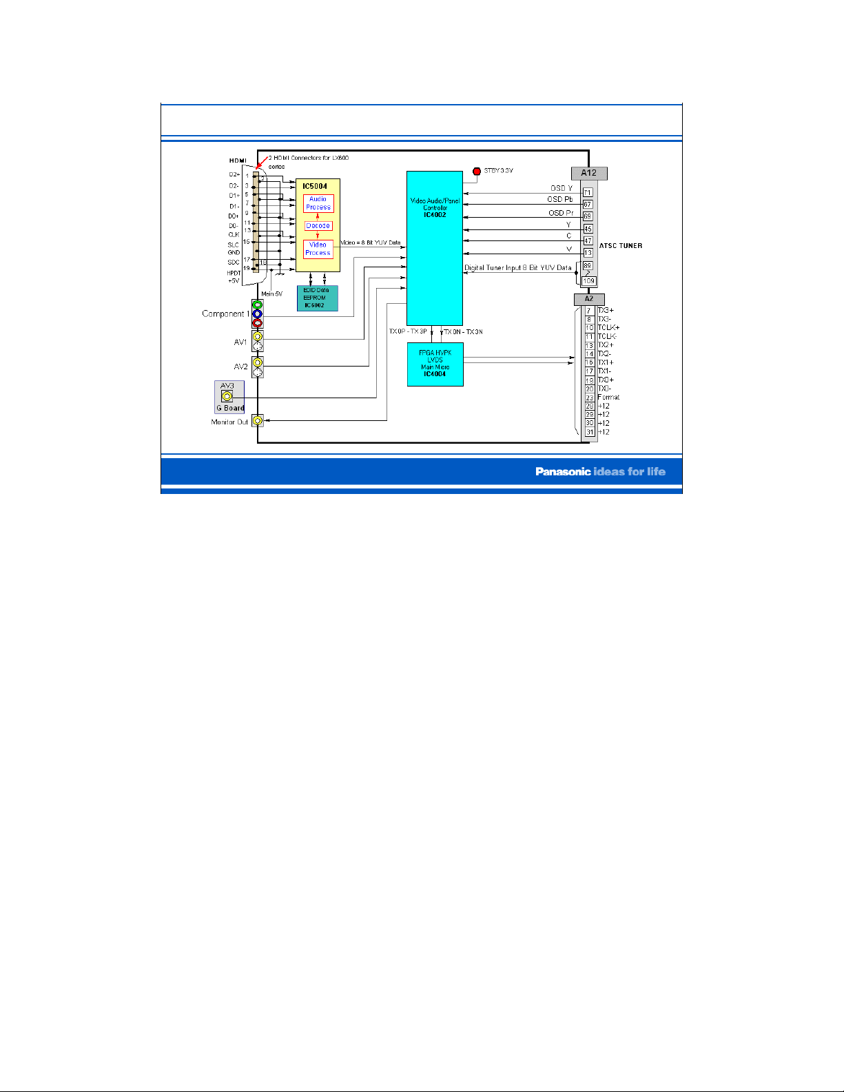
Video processing is performed on the A board. The A board incorporated
in these models is now responsible for signal processing, and system
control operation. The video processing function that had been performed
by the DG board of the previous models is now accomplished on the A
Board by IC4002. This IC is also responsible for selectively switching all
video inputs (Tuner, Component, Composite, S-Video, and HDMI). The
HDMI video is converted to an eight-bit YUV signal by the HDMI IF
receiver (IC5004) before being output to the video selector. IC5002
provides the copyright protection for the incoming HDMI signals. The
ATSC interface (DT board) processes the ATSC, NTSC, and QAM television
signals. The analog NTSC and digital ATSC or QAM signal of the DT board are
output to the A board via the connector DT12/A12. IC4002 is responsible for
processing all video, which includes image resizing, noise reduction, I/P
conversion and Gamma adjustment control. Although selected by a
different IC, the audio processing function is also performed by IC4002.
OSD is also generated by IC4002 and mixed with the video signal before
being output to IC4004. IC4004 is a Field Programmable Gate array
responsible for the pixel conversions and addressing of t he Ac tive Matrix
display within the LCD Panel. This IC also contains the low voltage
differential signaling (LVDS) transmitter, used for the conversion of the 8bit RGB video into a differential RGB output signal. The LVDS receiver
on the LCD panel (not shown in the drawing) converts the differential
RGB output signal from the A board into an 8-bit RGB signal that is
provided to the LCD Panel.
8
Page 9
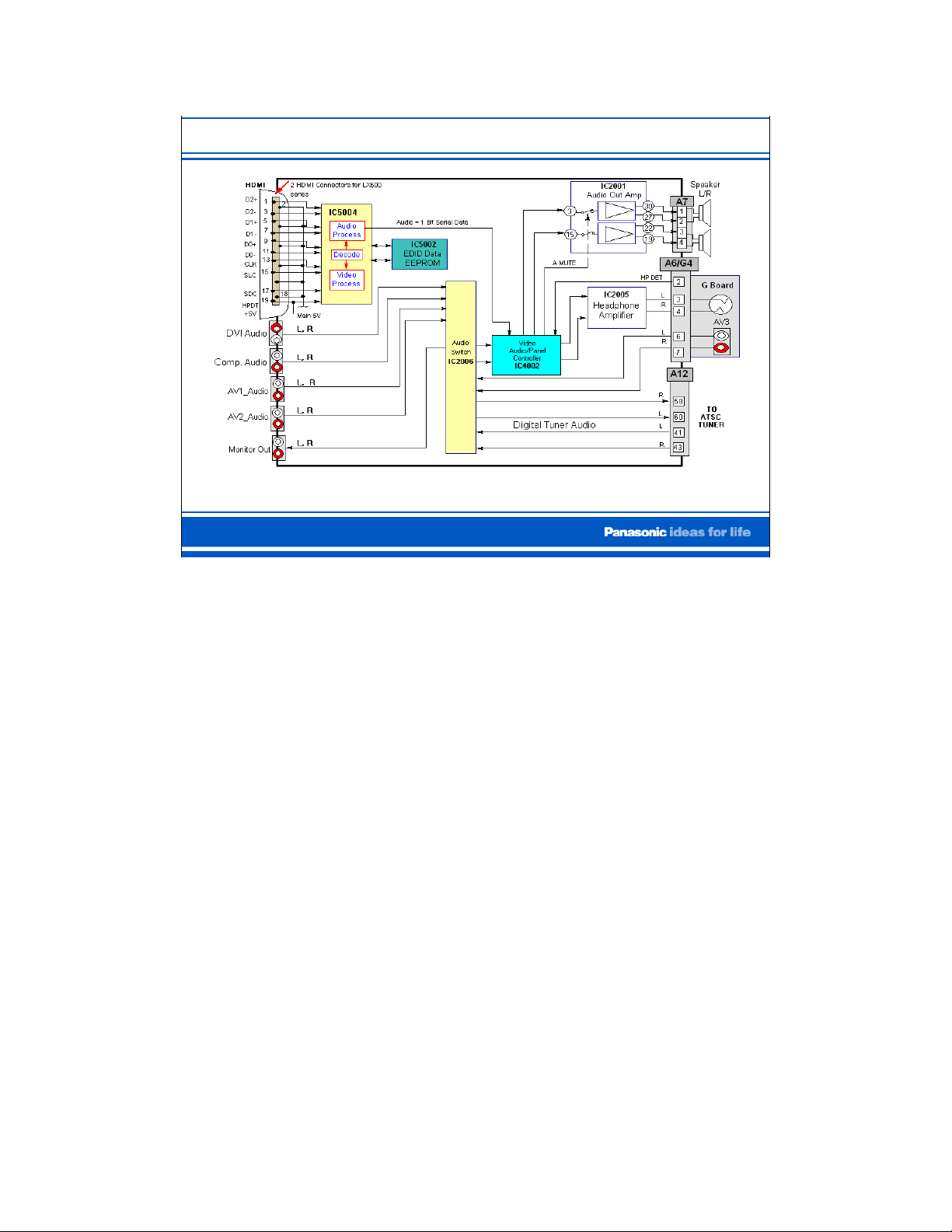
A
Board Audio Processing
Audio processing is performed on the A board. Audio signals from the
DVI, Component, and the Composite video input enter the Audio Switch
IC2006 where the desired input is selected. HDMI Audio is processed
and converted into a one bit digital audio format by the HDMI IF receiver,
IC5004. The HDMI audio bypasses the audio switch and enters IC4002
for selection and processing. The output of IC2006 is processed within
the Video/Audio controller IC4002. The Audio Output from the
Video/Audio controller is output to the speakers via the Audio Amplifier
IC2001 and pins 1 through 7 of connector A7. The Headphone amplifier
is activated when the headphones are plugged into the headphone jack
located on the G board. This action mutes the audio to the speakers by
disabling the Audio output Amplifier IC2001.
9
Page 10
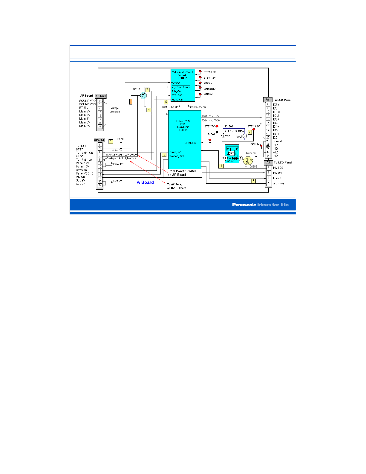
Power On Sequence
1.The Standby 7V (STB_7V) is generated on the P board (non- serviceable) when AC power
is applied. This can be measured on Pin 3 of Connector AP4/A4.
2.The STB_7V is regulated to 3.3 V on the Main board and applied to the Main Video and
Audio Controller IC4002.
3.Power on command by the remote control is not possible until the main power switch is
activated. When the Main Power Switch (AP Board) is activated, a active low ALL_OFF
signal is provided to the base of Q1151 via pin 7 of the connector AP4/A4. As a result
Q1151 turns on and a low is applied to the Key Scan Power input pin of IC4002. This
causes the unit to turn on, display a raster and become fully operational. The remote
control commands are now received and processed by the main unit. To continue
having full access via the remote control, the unit must be powered off by the remote
control, not by the power switch located on the main unit.
4.The Sub-On signal is issued by IC4002 on pin 8 of connector AP4. This signal is
responsible for pulling the contacts on the AC relay on the Power Board.
5.The Main_On signal is issued by IC4002 and provided to the AP board via pin 6 of
connector AP4/A4. It enables the Main 9V, Main 5V, and the Sound 18V (Not Shown in
the diagram) secondary power sources of the AP board. The Main_On signal is also
responsible for enabling the Main 3.3V regulator needed to power IC4004.
6.IC4004 provides the Panel_On signal that enables the Panel 12V regulator on the AP
board. It also provides the Inverter_On signal that enables the DC to AC inverter
circuitry on the LCD Panel.
7.The Inverter PWM signal and Current signal control the output voltage of the DC to AC
inverters that is used to power the CCFLTs. Increasing the on time of the INV_PWM
signal, which can be seen on pin 5 of connector A5, will increase the brightness of the
backlighting on the LCD Panel.
8.The INV_SOS signal is issued by the logic that resides on the LCD Panel if there is a
problem with the panel of inverter power supply.
10
Page 11

A
P Board Power Distribution
The AP Board is responsible for the regulation, distribution and
dissemination of all secondary voltages derived from the 24V and 10V
source supplies on the P Board. The 7V STBY voltage is present when
the unit is plugged into the AC outlet. When the main power switch is
activated, it is sensed on the main board by IC4002. A TV_SUB_ON
signal is subsequently issued in response, on pin 9 of connector AP4,
which activates the “Relay” signal on pin11 of connector AP2. This pulls
the contacts on the AC relay on the P board and allows for the output of
the 24V and 10V on that same connector. The TV_Main_ON signal
issued by IC4002, appears on pin 6 of connector AP4/A4 and provides
the output “Enable” for the 5V, 9V, and 20V switched mode power
supplies. Q7208 serves as a 24V detection line and provides an enable
for the Main_ on signal to function if 24V is detected. The panel 12V_On
signal provides the “Enable” for the Panel 12V logic and the enable for
the 24V inverters on the LCD Panel.
When a panel-on command is issued to turn on the Panel 12V switched
supply IC7212 located on the AP Board, transistor Q7805 turns on
causing Q7806 to turn off. As a result, the INV_ON pin of IC4004 on the
A board goes high. That same DC is applied to the LCD Panel’s inverter
input on pin 3 of connector A5 also on the A board.
The over voltage protection circuitry affiliated with each of the regulators,
is responsible for monitoring for excessive or over voltage conditions, and
is designed to turn off the AC power by disabling the SUB_ON signal
needed to turn on the AC relay. All voltages are accessible and can be
measured either on the connectors or on the highlighted jumper
locations.
11
Page 12

Main 5V Supply
The Main 5V, Main 9V, Sound 20V, and Panel 12V supplies are very similar
in their design and operation. Panasonic utilizes several Buck regulator
circuits to generate these voltages. The primary difference is that the
input voltage to the Main 5V regulator is 10V whereas the 9V, 20V, and
12V supplies use 24V.
1. Operation begins when the Main_On signal, derived from the
TV_Main_On (active low) signal turns off Q7303, providing the “Enable”
for operation of IC7205 on pin 5.
2. The 10V input voltage is switched between pins 1 and 2 at a frequency of
125Khz through the use of an internal oscillator and PWM circuit.
3. When the switch is closed, current flows through coil L7203 causing a
field buildup.
4. When the switch opens, current generated by the field collapses in L7203
and charges the capacitor C7255; D7231 acts as a ground return.
5. Voltage feedback and regulation is accomplished through the use of a
voltage divider, which consists of R7292 and R7293.
6. D7230 prevents peaks generated by L7203 from exceeding 10V and
destroying the IC.
7. Zener diode D7301 monitors the Main 5V output for over voltage and goes
into conduction if the output voltage becomes excessive. Diode D7302
which is reversed biased during normal operation goes into conduction
and trips the AC shutoff circuit.
12
Page 13

SUB 9V and 30V Tuner Supply
The SUB 9V and BT 30V Tuner sources are generated by the same switch
mode power supply IC, IC7209.
The supply encompasses the design of both Buck and Boost regulator
circuits.
1. A soft-on enable is provided on pin 5 of IC7209 during the initial power on
sequence as capacitor C7294 charges.
2. The 24V input is switched between pins one and two at a frequency of
125Khz.
3. The operation of the 9V supply is similar to that of the 5V supply.
4. D7602 is responsible for supplying the 9V to the capacitors when the
magnetic field within the coil collapses.
5. When the switch contact is open, the A side of coil L7204 goes negative,
providing a reference for the capacitors C7601, C7610, and C76 09 to
charge to 9V via the diode D7602.
6. The next time the switch is closed, the 24V appears at the A side of the
coil causing the same capacitors to charge to 24V. As a result the 24V
and 9V charges add up, resulting in the 30V output.
13
Page 14

A
P Board Protection Shutdown
The protection shutdown circuit is designed to monitor for a short or loss of
the 10V, 30V, Sound 18V,and the Panel VCC sources. If any of these
voltage sources go low, it will cause Q7210 to conduct. As a result, the
collector of Q7211 goes low to signal a shutdown condition to IC4002 on
the A board. The TV_SUB_ON pin of IC4002 goes low to de-activate the
AC relay on the P board.
14
Page 15

A
P Board Test Point Locations
This page shows the test points that can be accessed to troubleshoot the AP
board.
15
Page 16

A
P Board LCD Power Distribution
Connector AP1 provides the switched 24V from the power unit to the LCD
Panel via connectors AP5 and AP7. The 24V can be monitored on
connector AP5 or on jumper JS7455.
16
Page 17

Adjustment Procedure
How to enter adjustment mode
While pressing the VOLUME DOWN button of the main
unit, press the RECALL button of the remote control
transmitter three times in a row within two seconds.
Adjustment method.....Use the remote control.
# 1. button...Main items Selection in forward direction
# 2. button...Main items Selection in reverse direction
# 3. button...Sub items Selection in forward direction
# 4. button...Sub items Selection in reverse direction
Cancellation
To exit the adjustment mode, turn the unit off using the power button of the
remote control or the main power switch of the main unit.
17
Page 18

Adjustment
Main Item
PCT-ADJ
WB-ADT
OPTION
STB-CAS
Sub Item
COLOR
R-Y-A
R-Y-G
BACK-L
TINT
B-CENT
G-CENT
R-CENT
B-GAIN
G-GAIN
R-GAIN
OPTDD
BOOT
Remarks
Video level (RF, video, component)
Video level (RF, video, component)
Video level (RF, video, component)
Tint Adjustment
Sub Color
Sub Tint
Sub Back Light
Sub Bright
B-Y Gain
R-Y Demodulation axis
WHITE 100% (Not ADJ)
RED 100% (Not ADJ)
Remarks
Sample Data
OFF
2E
73
FA
DD
B7
8D
65
C2
E0
FF
DD
ROM
Generally the PCT _ADJ for the color, Backlighting, and Tint is all that is
generally required.
18
Page 19

How to Access the Self-check Screen
Access
1. Place the unit in TV mode.
2. While pressing the VOLUME
DOWN button on the main
unit, press the SLEEP button
on the remote controller unit
simultaneously
Exit
1. Press one of the channel
selection buttons to return to
the normal screen.
.
To get into the Self-check mode, press and hold down the VOLUME DOWN
button on the front of the unit, and the SLEEP button on the remote control.
Hold the buttons down for at least three seconds. The unit self tunes to
channel 3. The word “SELF-CHECK“, followed by a graphic OSD appears at
the center of the screen.
All Customer settings (parameters) will be erased. Access the self-check
screen to reset the unit. This brings the unit back to factory default.
If the Communication Control port of an IC is addressed and a response is
not received by the system control IC, then " - - " or “NG” will appear in
place of " OK ".
19
Page 20

No Video From Tuner
Check and see if the Tuner Activity
indicator is on RED. It is visible through
the holes on the cover plate.
Replace Tuner
Yes
Are SUB 9V
SUB 5V
OK ?
Replace defective Regulator and
biasing components. Reference
the power distribution diagram on
Slide 10 for location.
Yes
Check for the BT 30V, SUB 9V, &,
SUB5V voltages on connector AP3
of the AP board. Refer to the AP Board
Yes
No
Is the Tuner
Activity
indicator on?
No
test point locations on Slide 13.
Is the
BT30V
OK ?
No
Check the cathodes of D7601 & D7602
on the AP Board. Cathode of D7601
should measure 30V. Replace defective
component
.
20
Page 21

No Video
Blue Screen
No Video, Dark Blue Screen
Try using a different video input source.
Try the Tuner, Component, S-Video or
HDMI input.
Replace defective Regulator and
biasing components. Reference
the power distribution diagram on
Slide 10 for location.
Does any
input
work?
Check for the BT 30V, SUB 9V, &,
SUB5V voltages on connector AP3
of the AP board. Refer to the AP Board
test point locations on Slide 13.
No
BT30V,
SUB9V
SUB5V
OK ?
To next page.
Yes
No
Yes
Check the video input connections and
termination points for a possible cold
solder joint or connection problem.
Did this
fix the
problem?
No
Replace the A Board
Yes
Problem Solved
21
Page 22

No Video, Dark Blue Screen (Continued)
From the last page
Replace the A Board.
From where it sits on the A board in order to
access the LVDS connector. There are four
No
Remove Tuner Board
screws that need to be removed.
Check for LVDS activity on Pins
6, 8, 12, 14, & 16 (orange wires)
of connector A2 on the A board.
Does the LVDS
Signal
Look OK ?
Yes
Replace the Panel.
22
Page 23

No Audio
Problem
Solved
A Board
Determine which audio input is
defective. Check for poor solder
connections in the vicinity of the
audio connection in question.
Yes
Is the Audio
OK ?
No
Change the A board.
Try using a different audio input
source. Try the Tuner, Component,
S Video or HDMI input .
Yes
Are other
Audio inputs
OK ?
Check the L/R speaker
output connection.
Reseat connector A7.
Does this fix
the Audio
problem?
Check for an audio signal on pins
1, 2, 3, &, 4 of
Connector A7. Refer to Slide 8.
See Next Page.
No
Yes
Problem
Solved
No
23
Page 24

No Audio
From Last Page.
Check for broken connector
A7 located on the A board.
Yes
Check for 20V on pins 2 & 3 of
connector AP3/A3 or jumper J116.
Is an audio
signal present?
Is the Voltage
~20V
Yes
Change the A Board.
No
No
Check regulator IC7218 on the AP
Board. Replace if defective.
24
Page 25

No Power
Refer to AP Board test point locations
Refer to AP Board test point locations
Slide 13
Slide 13
Turn on the Main
Power Switch.
Check for the primary
24V and 10V output.
24V & 10V
Yes
OK?
No
Replace the
P Board.
Check for 6V on pin 11 of
connector AP2 (RELAY.)
Yes
The ALL Off signal on Pin 7
of connector AP4 should go
low when the Main Power
6V
Present?
No
switch is depressed.
Pin 7 low?
See Next Page.
Yes
No
Replace the
Main Switch.
Yes
Can an audible
click be heard
from the Power
relay?
No
Standby 7V
JS7963
OK?
No
Check for STBY 7V on pin 12 of
connector AP2.
7V
Present?
No
If connector is good, replace
the P Board.
Yes
25
Page 26

No Power
efer to the AP Board test point locations
efer to the AP Board test point locations
Slide 13
Slide 13
Make sure connector A4 of the A
board is seated properly. Unit will
exhibit this condition if the connector
From Last Page.
is unplugged.
Does the unit
come on?
Problem solved.
No
Replace the A board.
Yes
26
Page 27

OF POWER
LED FLASHES
2
Power LED Flashes
SUSPECTED BOARDPOSSIBLE CIRCUIT (MICRO PIN)NUMBER
P, PanelINVERTER SOS, NO BACKLIGHT
DETECTION (FPGA pin 6)
A, P24V down VCTP (pin 106)5
AP9V down VCTP (pin 1)6
7
VCTP (pin 105)
8
105)
AP, ASOURCE VOLTAGE ABNORMALITY
A FPGA ABNORMALITY VCTP (pin
27
Page 28

LED Blinks Seven Times
Refer to the AP Board test point locations
Conduct a voltage check on the
AP Board.
Refer to the AP Board test point locations
Slide 13
Slide 13
Sound
20V OK?
Main 9V
OK?
5V OK?
30V Tuner?
No
Check and replace if necessary
IC7218 and biasing components.
Check and replace if necessary
IC7210 and biasing components.
No
Check and replace if necessary
IC7205 and biasing components.
No
Check and replace if necessary
D7601 or D7602 and biasing components.
28
Page 29

LED Blinks Twice Every 5 Seconds
Check for 24V on jumper JS7455
or on connector AP5 pins 1-8.
24V OK?
Unplug connector AP5 and measure
for 24V on jumper JS7455 or on
connector AP5 pins 1-8.
24V OK?
END
Yes
No
No
Confirm that the Inverter_SOS
signal on pin 2 of connector A5 is
Active High prior to changing the
LCD Panel. Use a Peak Hold
Voltmeter for measurement.
Change the P-board.
Refer to AP Board test point locations
Refer to AP Board test point locations
Slide 13
Slide 13
29
Page 30

Examples of Defective Panels
Distorted Partial Picture
Horizontal Lines
Green, Red, or Blue Shading
30
Page 31

Pedestal Removal
31
Page 32

Pedestal Removal
32
Page 33

The End
The End
33
 Loading...