

Page 1
ORDER NO.VM0712053CE
B27
SD Card / Hard Disk Video Camera
Model No.SDR-H40P
SDR-H40EG
SDR-H40E
SDR-H40EB
SDR-H40EP
SDR-H40EF
SDR-H40GC
SDR-H40GN
SDR-H40PL
SDR-H48GK
SDR-H40PC
VOL.1
Colour
(S)....................Silver Type
© 2007 Matsushita Electric Industrial Co., Ltd. All
rights reserved. Unauthorized copying and
distribution is a violation of law.
Page 2
SDR-H40P
CONTENTS
Page Page
1 Safety Precaution 3
1.1. General Guidelines
2 Warning
2.1. Prevention of Electrostatic Discharge (ESD) to
Electrostatic Sensitive (ES) Devices
2.2. Service caution based on legal restrictions
2.3. Caution for AC Cord (For EB/GC)
2.4. How to Replace the Lithium Battery (PROCEDURE)
2.5. How to Recycle the Lithium Battery (U.S. Only)
3 Service Navigation
3.1. Service Information
3.2. Precautions for Handling HDD
3.3. Formatting HDD
4 Specifications
5 Location of Controls and Components
6 Service Mode
6.1. Error Display
6.2. Service Menu
6.3. About Default Setting
7 Service Fixture & Tools
7.1. Service Tools and Equipment
8 Disassembly and Assembly Instructions
8.1. Disassembly Frow Chart
8.2. P.C.B. Layout
8.3. Disassembly Procedures
8.4. Disassembly Procedures of Camera Lens Unit
9 Measurements and Adjustments
3
4
4
5
6
7
8
9
9
10
14
15
16
18
18
18
23
24
24
25
25
25
26
31
9.1. EEPROM Data for spare parts of the MAIN P.C.B.
9.2. Service Positions
9.3. Location for Connectors of the Main P.C.B.
9.4. Electrical Adjustment Procedures
10 Maintenance
10.1. Cleaning Lens and LCD Panel
11 Schematic Diagrams
11.1. OVERALL SCHEMATIC DIAGRAM
11.2. INTERCONNECTION SCHEMATIC DIAGRAM
11.3. FRONT SCHEMATIC DIAGRAM
11.4. LCD BACKLIGHT SCHEMATIC DIAGRAM
11.5. REAR CASE SCHEMATIC DIAGRAM
11.6. SHAFT FPC SCHEMATIC DIAGRAM
11.7. HDD FPC UNIT SCHEMATIC DIAGRAM
11.8. CCD SCHEMATIC DIAGRAM
11.9. SIDE L UNIT SCHEMATIC DIAGRAM
11.10. SD SCHEMATIC DIAGRAM
12 Printed Circuit Board
12.1. SD P.C.B.
12.2. FRONT P.C.B.
12.3. LCD BACKLIGHT P.C.B.
13 Parts and Exploded Views
13.1. Exploded Views
13.2. Replacement Parts List
32
32
32
34
35
39
39
41
41
42
43
44
45
45
45
46
47
48
49
49
50
51
53
53
58
2
Page 3
1 Safety Precaution
1.1. General Guidelines
1. IMPORTANT SAFETY NOTICE
There are special components used in this equipment which are important for safety. These parts are marked by in the
Schematic Diagrams, Circuit Board Layout, Exploded Views and Replacement Parts List. It is essential that these critical parts
should be replaced with manufacturer’s specified parts to prevent X-RADIATION, shock fire, or other hazards. Do not modify
the original design without permission of manufacturer.
2. An Isolation Transformer should always be used during the servicing of AC Adaptor whose chassis is not isolated from the AC
power line. Use a transformer of adequate power rating as this protects the technician from accidents resulting in personal injury
from electrical shocks. It will also protect AC Adaptor from being damaged by accidental shorting that may occur during
servicing.
3. When servicing, observe the original lead dress. It a short circuit is found, replace all parts which have been overheated or
damaged by the short circuit.
4. After servicing, see to it that all the protective devices such as insulation barriers, insulation papers shields are properly
installed.
5. After servicing, make the following leakage current checks to prevent the customer from being exposed to shock hazards.
1.1.1. Leakage Current Cold Check
1. Unplug the AC cord and connect a jumper between the two prongs on the plug.
2. Measure the resistance value, with an ohmmeter, between the jumpered AC plug and each exposed metallic cabinet part on
the equipment such as screwheads, connectors, control shafts, etc. When the exposed metallic part has a return path to the
chassis, the reading should be between 1MW and 5.2MW. When the exposed metal does not have a return path to the chassis,
the reading must be infinity.
SDR-H40P
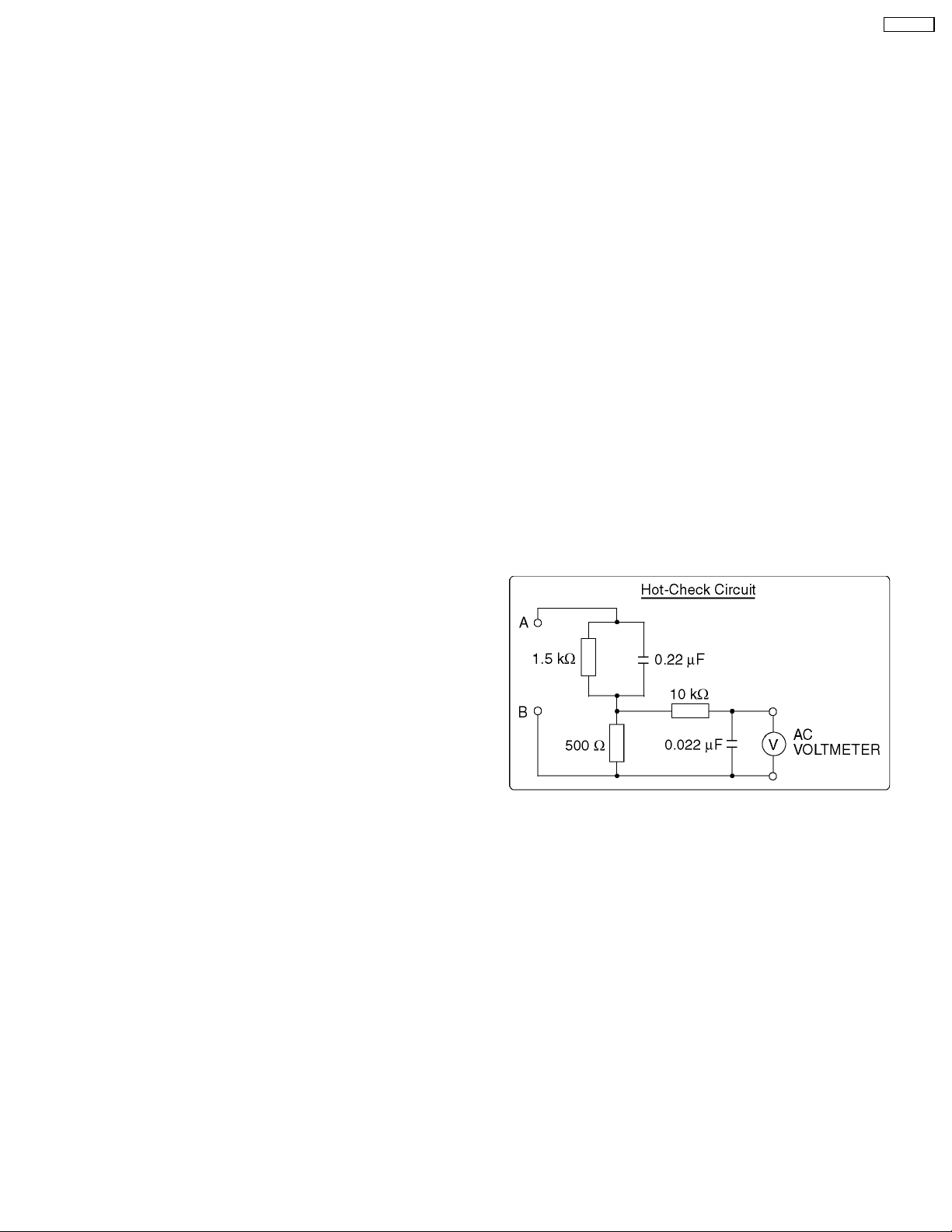
1.1.2. Leakage current hot check (See Figure 1)
1. Plug the AC cord directly into the AC outlet. Do not use an
isolation transformer for this check.
2. Connect “A” to exposed metallic part on the set. And
connect “B” to a good earth ground, as shown in Figure 1.
3. Use an AC voltmeter, with 1 kW/V or more sensitivity, to
measure the potential across the resistor.
4. Check each exposed metallic part, and measure the
voltage at each point.
5. Reverse the AC plug in the AC outlet and repeat each of the
above measurements.
6. The potential at any point should not exceed 0.25 V RMS.
A leakage current tester (Simpson Model 229 or equivalent)
may be used to make the hot checks, leakage current must
not exceed 1/2 mA. In case a measurement is outside of
the limits specified, there is a possibility of a shock hazard,
and the equipment should be repaired and rechecked
before it is returned to the customer.
Figure 1
3
Page 4
SDR-H40P
2 Warning
2.1. Prevention of Electrostatic Discharge (ESD) to Electrostatic Sensitive
(ES) Devices
Some semiconductor (solid state) devices can be damaged easily by static electricity. Such components commonly are called
Electrostatic Sensitive (ES) Devices. Examples of typical ES devices are integrated circuits and some field-effect transistors and
semiconductor “chip” components. The following techniques should be used to help reduce the incidence of component damage
caused by electrostatic discharge (ESD).
1. Immediately before handling any semiconductor component or semiconductor-equipped assembly, drain off any ESD on your
body by touching a known earth ground. Alternatively, obtain and wear a commercially available discharging ESD wrist strap,
which should be removed for potential shock reasons prior to applying power to the unit under test.
2. After removing an electrical assembly equipped with ES devices, place the assembly on a conductive surface such as
aluminum foil, to prevent electrostatic charge buildup or exposure of the assembly.
3. Use only a grounded-tip soldering iron to solder or unsolder ES devices.
4. Use only an antistatic solder removal device. Some solder removal devices not classified as “antistatic (ESD protected)” can
generate electrical charge sufficient to damage ES devices.
5. Do not use freon-propelled chemicals. These can generate electrical charges sufficient to damage ES devices.
6. Do not remove a replacement ES device from its protective package until immediately before you are ready to install it. (Most
replacement ES devices are packaged with leads electrically shorted together by conductive foam, aluminum foil or comparable
conductive material).
7. Immediately before removing the protective material from the leads of a replacement ES device, touch the protective material
to the chassis or circuit assembly into which the device will be installed.
CAUTION:
Be sure no power is applied to the chassis or circuit, and observe all other safety precautions.
8. Minimize bodily motions when handling unpackaged replacement ES devices. (Otherwise harmless motion such as the
brushing together of your clothes fabric or the lifting of your foot from a carpeted floor can generate static electricity (ESD)
sufficient to damage an ES device).
4
Page 5
2.2. Service caution based on legal restrictions
2.2.1. General description about Lead Free Solder (PbF)
The lead free solder has been used in the mounting process of all electrical components on the printed circuit boards used for this
equipment in considering the globally environmental conservation.
The normal solder is the alloy of tin (Sn) and lead (Pb). On the other hand, the lead free solder is the alloy mainly consists of tin
(Sn), silver (Ag) and Copper (Cu), and the melting point of the lead free solder is higher approx.30 degrees C (86°F) more than that
of the normal solder.
Definition of PCB Lead Free Solder being used
The letter of “PbF” is printed either foil side or components side on the PCB using the lead free solder.
(See right figure)
Service caution for repair work using Lead Free Solder (PbF)
· The lead free solder has to be used when repairing the equipment for which the lead free solder is used.
(Definition: The letter of “PbF” is printed on the PCB using the lead free solder.)
· To put lead free solder, it should be well molten and mixed with the original lead free solder.
· Remove the remaining lead free solder on the PCB cleanly for soldering of the new IC.
· Since the melting point of the lead free solder is higher than that of the normal lead solder, it takes the longer time to melt
the lead free solder.
· Use the soldering iron (more than 70W) equipped with the temperature control after setting the temperature at 350±30
degrees C (662±86°F).
Recommended Lead Free Solder (Service Parts Route.)
· The following 3 types of lead free solder are available through the service parts route.
RFKZ03D01K-----------(0.3mm 100g Reel)
RFKZ06D01K-----------(0.6mm 100g Reel)
RFKZ10D01K-----------(1.0mm 100g Reel)
SDR-H40P
Note
* Ingredient: tin (Sn), 96.5%, silver (Ag) 3.0%, Copper (Cu) 0.5%, Cobalt (Co) / Germanium (Ge) 0.1 to 0.3%
5
Page 6
SDR-H40P
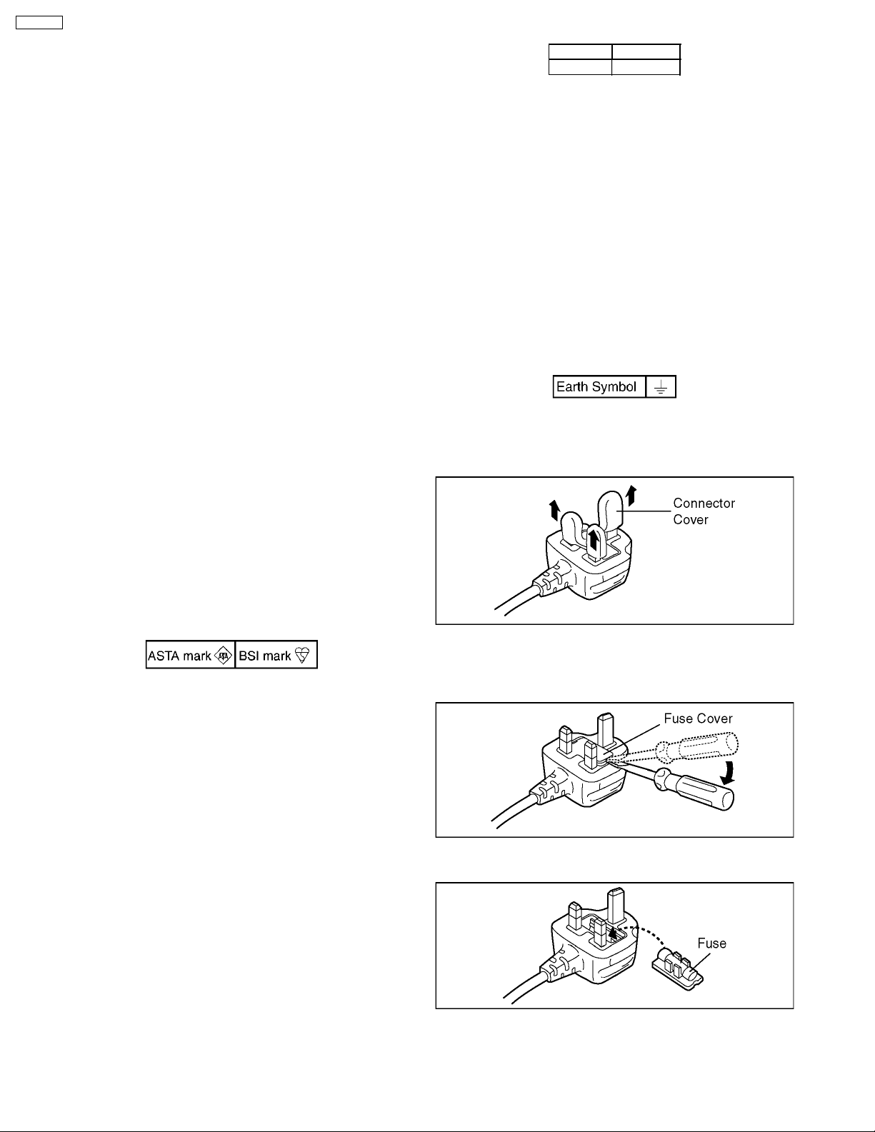
2.3. Caution for AC Cord
(For EB/GC)
Blue Neutral
Brown Live
2.3.1. Information for your safety
IMPORTANT
Your attention is drawn to the fact that recording of prerecorded tapes or discs or other published or broadcast
material may infringe copyright laws.
WARNING
To reduce the risk of fire or shock hazard, do not expose
this equipment to rain or moisture.
CAUTION
To reduce the risk of fire or shock hazard and annoying
interference, use the recommended accessories only.
FOR YOUR SAFETY
DO NOT REMOVE THE OUTER COVER
To prevent electric shock, do not remove the cover. No user
serviceable parts inside. Refer servicing to qualified service
personnel.
2.3.2. Caution for AC mains lead
For your safety, please read the following text carefully.
This appliance is supplied with a moulded three-pin mains plug
for your safety and convenience.
A 5-ampere fuse is fitted in this plug.
Should the fuse need to be replaced please ensure that the
replacement fuse has a rating of 5 amperes and it is approved
by ASTA or BSI to BS1362
Check for the ASRA mark or the BSI mark on the body of the
fuse.
As the colours of the wires in the mains lead of this appliance
may not correspond with the coloured markings identifying the
terminals in your plug, proceed as follows:
The wire which is coloured BLUE must be connected to the
terminal in the plug which is marked with the letter N or
coloured BLACK.
The wire which is coloured BROWN must be connected to the
terminal in the plug which is marked with the letter L or coloured
RED.
Under no circumstances should either of these wires be
connected to the earth terminal of the three pin plug, marked
with the letter E or the Earth Symbol.
2.3.2.2. Before use
remove the Connector Cover as follows.
If the plug contains a removable fuse cover you must ensure
that it is refitted when the fuse is replaced.
If you lose the fuse cover, the plug must not be used until a
replacement cover is obtained.
A replacement fuse cover can be purchased from your local
Panasonic Dealer.
If the fitted moulded plug is unsuitable for the socket outlet in
your home then the fuse should be removed and the plug cut
off and disposed of safety.
There is a danger of severe electrical shock if the cut off plug
is inserted into any 13-ampere socket.
If a new plug is to be fitted please observe the wiring code as
shown below.
If in any doubt, please consult a qualified electrician.
2.3.2.1. Important
The wires in this mains lead are coloured in accordance with
the following code:
2.3.2.3. How to replace the Fuse
1. Remove the Fuse Cover with a screwdriver.
2. Replace the fuse and attach the Fuse cover.
6
Page 7
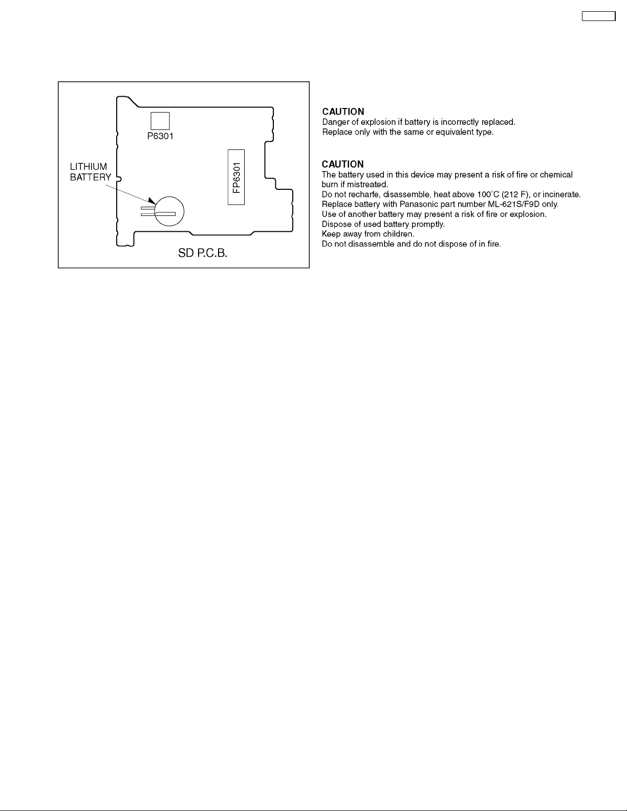
2.4. How to Replace the Lithium Battery (PROCEDURE)
1. Remove the SD P.C.B.. (Refer to Disassembly Procedures.)
2. Unsolder the Lithium Battery “ML-621S/F9D” and then replace the new one. (See Figure B1.)
Fig. B1
Note:
The lithium battery is a critical component. (Type No.: ML-621S/F9D Manufactured by Panasonic.)
It must never be subjected to excessive heat or discharge.
It must therefore only be fitted in equipment designed specifically for its use.
Replacement batteries must be of the same type and manufacture.
They must be fitted in the same manner and location as the original battery, with the correct polarity contacts observed.
Do not attempt to re-charge the old battery or re-use it for any other purpose.
It should be disposed of in waste products destined for burial rather than incineration.
SDR-H40P
7
Page 8
SDR-H40P
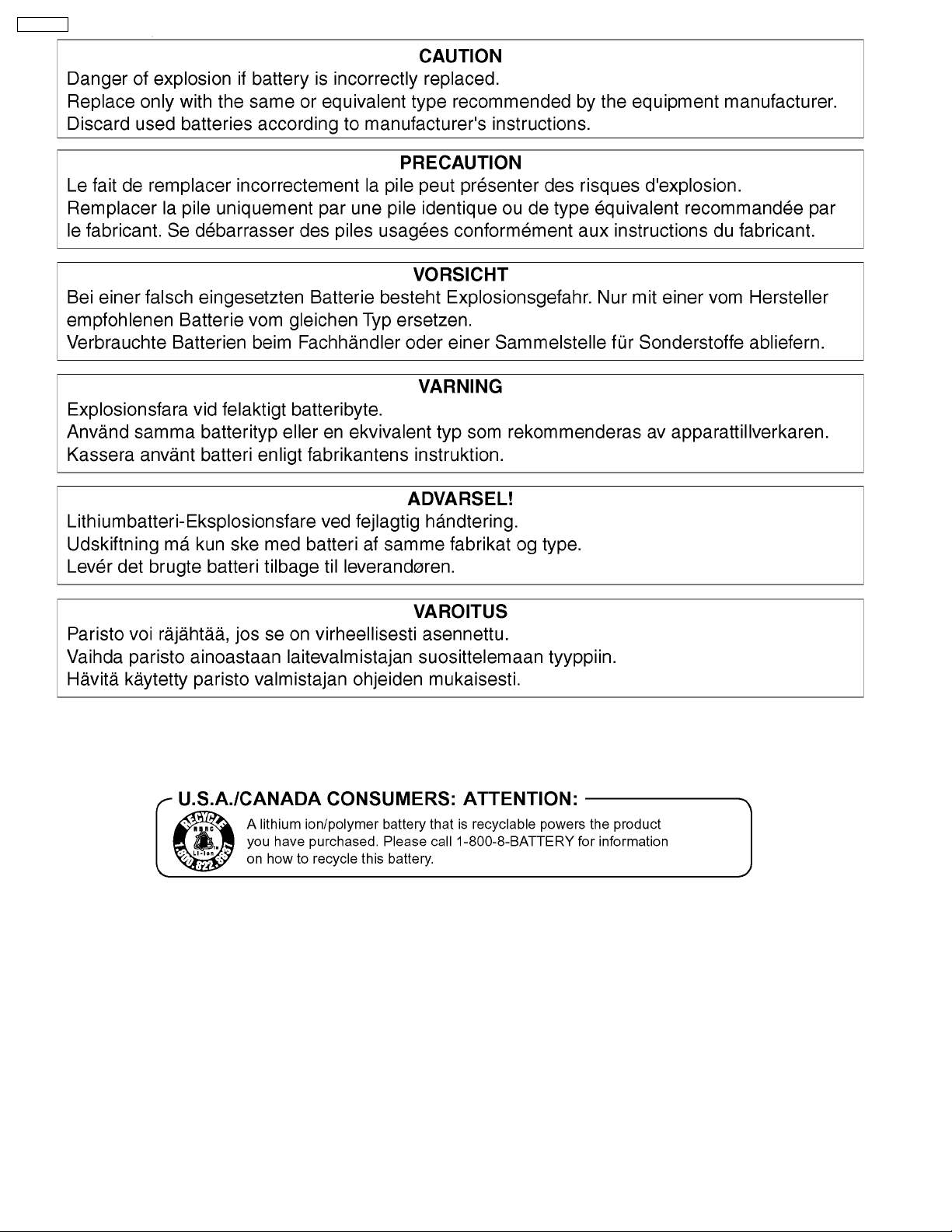
2.5. How to Recycle the Lithium Battery (U.S. Only)
8
Page 9

3 Service Navigation
3.1. Service Information
This service manual contains technical information which will allow service personnel´s to understand and service this model.
Please place orders using the parts list and not the drawing reference numbers.
If the circuit is changed or modified, this information will be followed by supplement service manual to be filed with original service
manual.
Notes 1:
1. VSK0697 is indicated on AC Adapter used on the following models:
SDR-H40P/PC/PL.
However, the AC Adapter replacement part number is DE-A51BA which should be used when ordering.
2. VSK0698 is indicated on AC Adapter used in the following models:
SDR-H40EG/E/EB/EP/EF/GC/GN.
However, the AC Adapter replacement part number is DE-A51CA which should be used when ordering.
3. VSK0698 is indicated on AC Adapter used on the following model:
SDR-H48GK.
However, the AC Adapter replacement part number is DE-A51DA which should be used when ordering.
Notes 2:
1) This service manual does not contain the following information, because of the impossibility of sevicing at component level.
1. Schematic Diagram, Block Diagram and P.C.B. layout of Main P.C.B.
2. Parts List for individual parts of Main P.C.B.
SDR-H40P
2) The following category are recycle module part. Please send them to Central Repair Center.
*Main P.C.B. (LSEP8443A1: SDR-H40P/PC/PL)
(LSEP8443P1: SDR-H40EG/E/EB/EP/EF/GC/GN, SDR-H48GK)
When a part replacement is required for repairing each Main P.C.B., replace the assembly parts.
(Main P.C.B.)
The following circuits are contained in Main P.C.B.
1. Main Connection Circuit
2. AVIO Circuit
3. Video Circuit
4. Memory Circuit
5. USB Host Circuit
6. LCD Circuit
7. Power Circuit
8. HDD G-Sensor Circuit
9. Lens Drive Circuit
10. TG/AFE Circuit
11. SYSCON Circuit
12. Sub SYSCON Circuit
9
Page 10
SDR-H40P
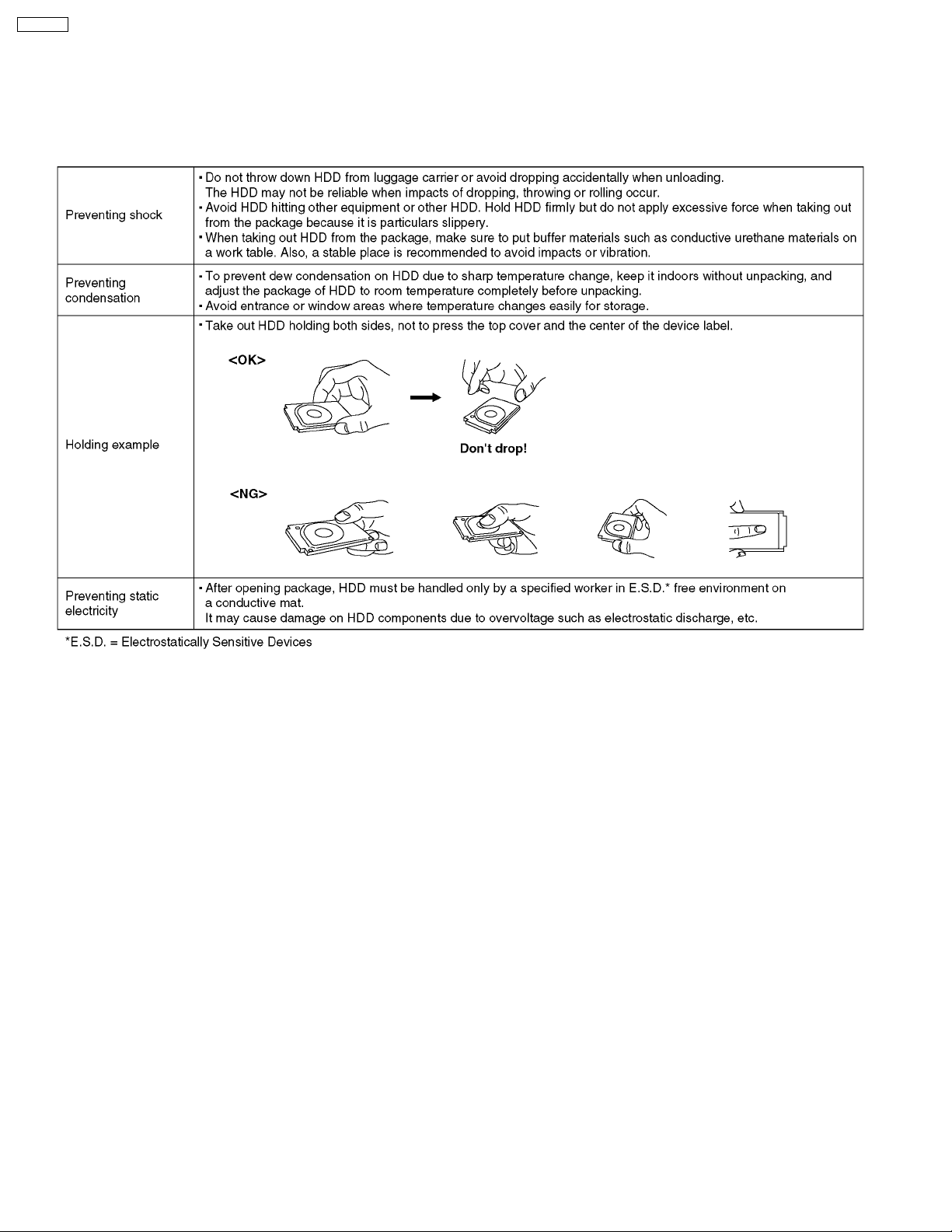
3.2. Precautions for Handling HDD
1. Handle HDD very carefully to prevent the static electricity and shock.
2. Set the HDD quickly after taking it out from the package. Make sure to put the HDD on buffer materials, etc.
3.2.1. Precautions at incoming process and for opening packages
10
Page 11
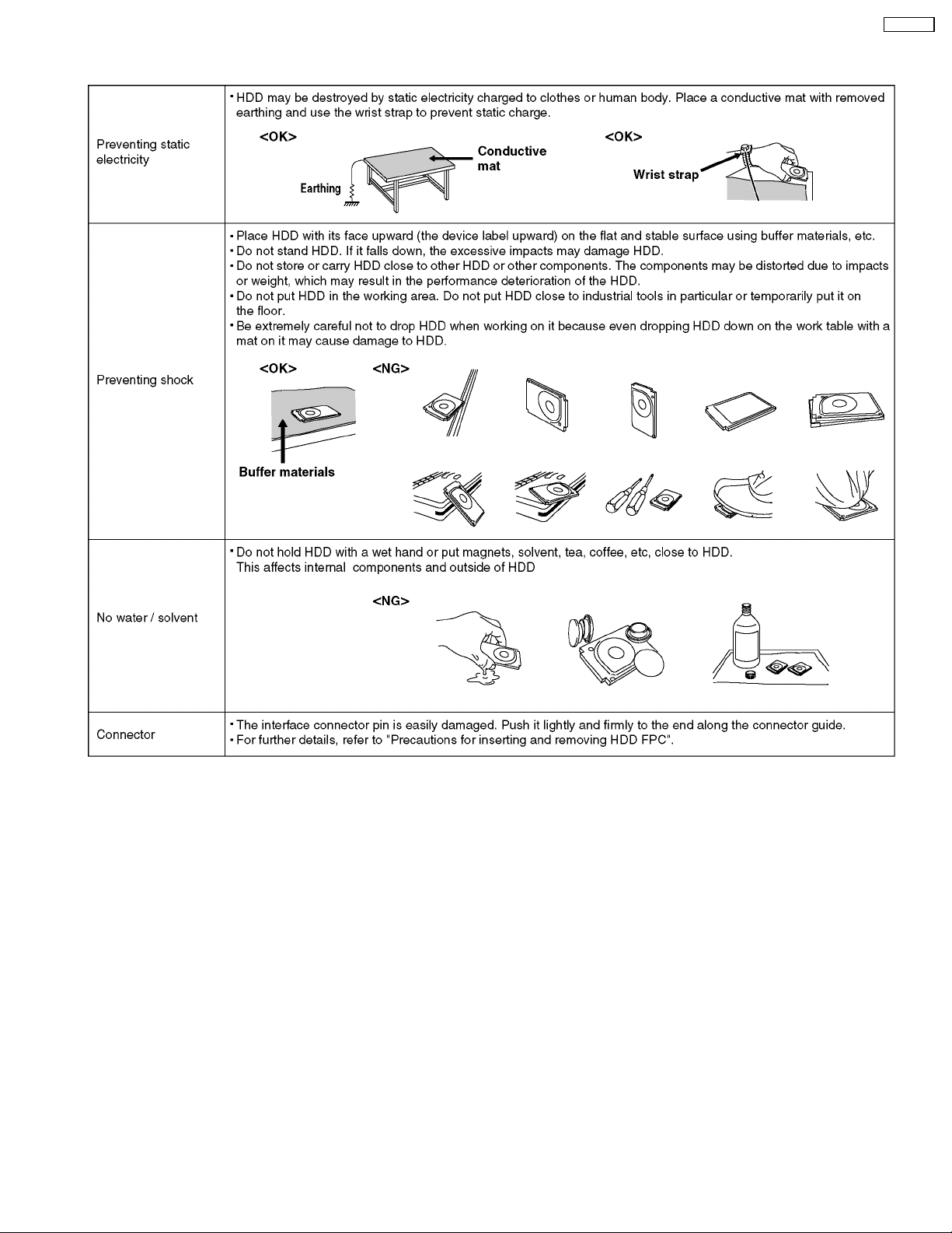
3.2.2. Precautions for installing HDD
SDR-H40P
11
Page 12
SDR-H40P
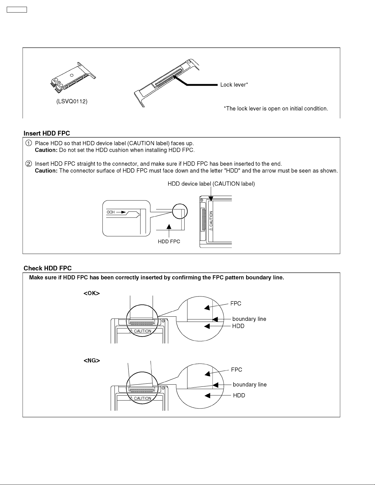
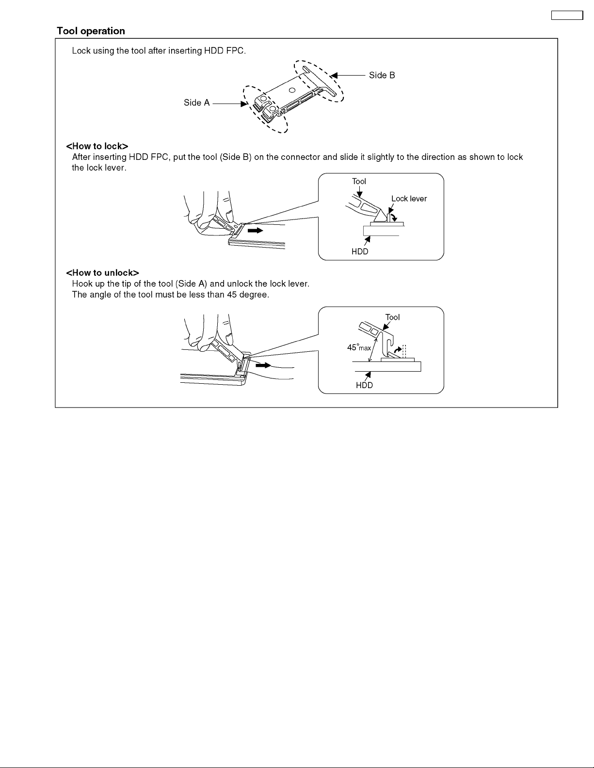
3.2.3. Precautions for inserting and removing HDD FPC
Make sure to use the tool (LSVQ0112) when locking and unlocking the lock lever of HDD FPC connector.
Do not lock the lock lever without inserting HDD FPC. Otherwise, the connector may be damaged.
12
Page 13
SDR-H40P
Make sure to use the tool (LSVQ0112) when opening and closing the lock lever.
*See "" (Fig. D4) for attaching to the unit.
13
Page 14
SDR-H40P
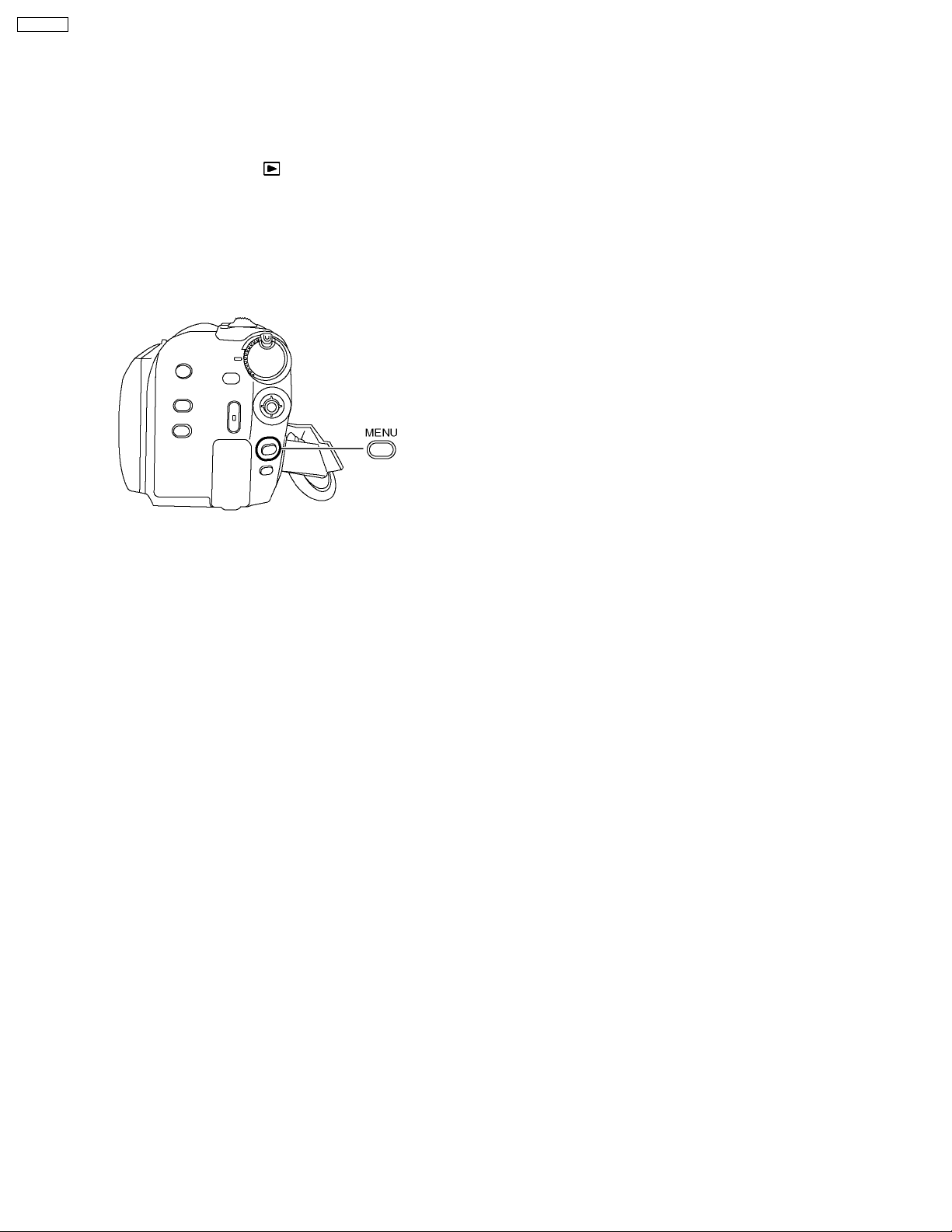
3.3. Formatting HDD
When HDD is exchanged, format HDD as the procedure below.
Without formatting, the error message appears on the LCD display when accessing HDD.
<Formatting procedure>
Rotate the mode dial to select
Select [HDD] in [MEDIA SELECT].
1. Press the MENU button, then
select [SETUP] ®®®®
[FORMAT HDD] ®®®® [YES] and
press the joystick.
2. When the confirmation message
appears, select [YES], then press
the joystick.
· When formatting is complete, press the MENU
button to exit the message screen.
Note:
· During formatting, do not turn this unit off.
· When you format the HDD, use a battery with
sufficient battery power or the AC adaptor.
· During formatting, do not cause any vibrations
or impacts to this unit.
.
14
Page 15
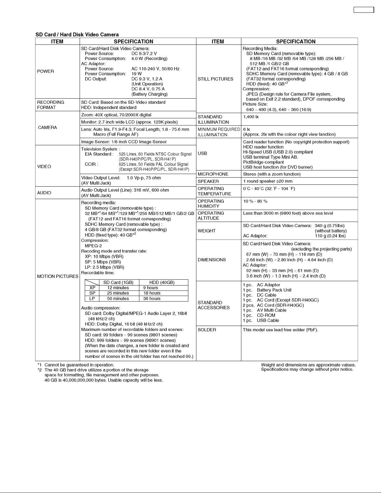
4 Specifications
SDR-H40P
15
Page 16
SDR-H40P
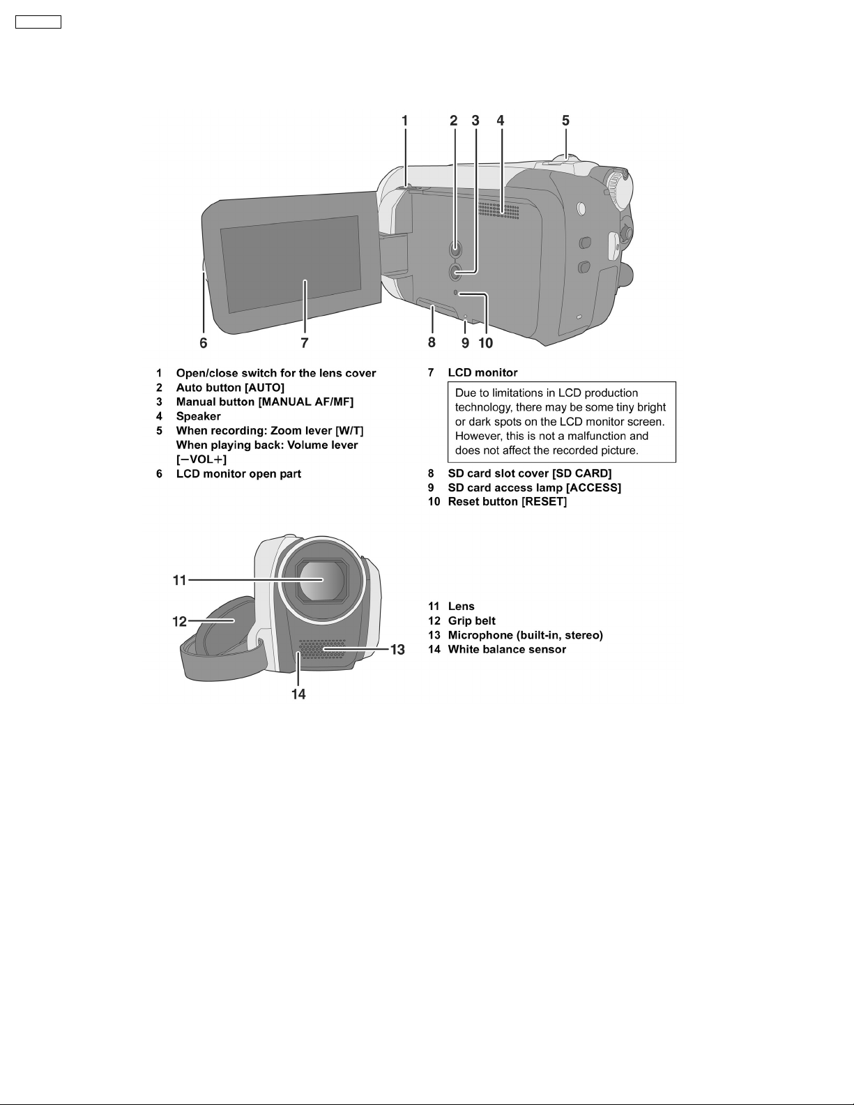
5 Location of Controls and Components
Followings are the Location of Controls and Components for SDR-H40P/PC as a sample.
For other models, refer to each Operatin Instructions.
16
Page 17
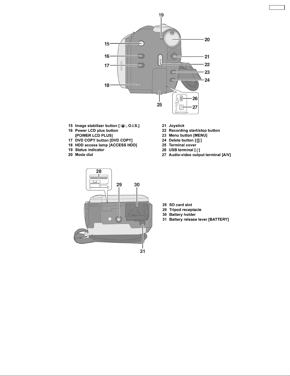
SDR-H40P
17
Page 18
SDR-H40P
6 Service Mode
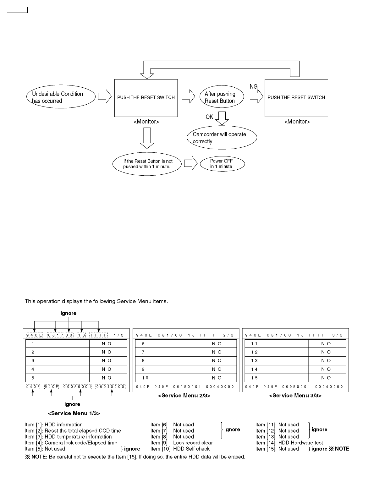
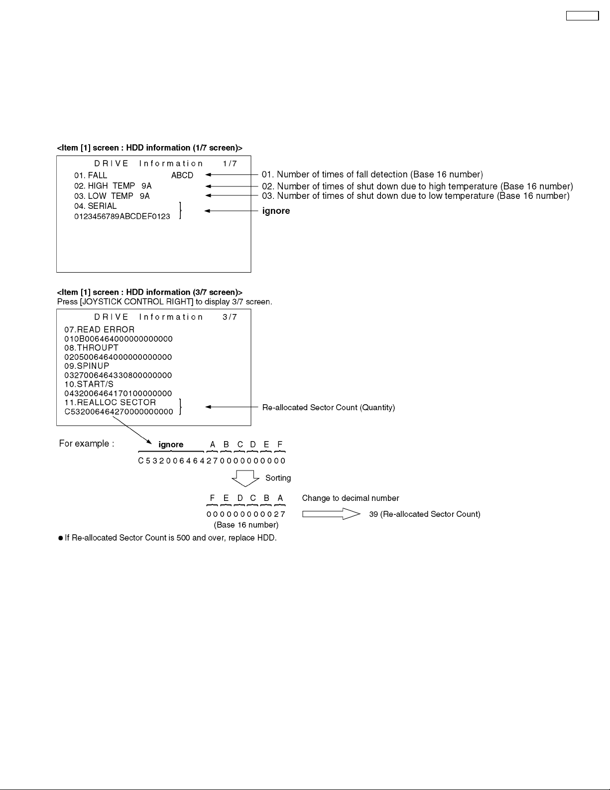
6.1. Error Display
"PUSH THE RESET SWITCH" is displayed automatically on the LCD Monitor when an undesirable condition has occurred.
Fig. 1
Note:
When "PUSH THE RESET SWITCH" is displayed repeatedly, service is required. Check the Error Code which is listed in the
Service Menu.
6.2. Service Menu
When abnormal detection contents are confirmed, do the following operation. Automatic diagnosis code will bedisplayed. (Service
Menu)
To enter the Service Menu
Push the [DELETE], [JOYSTICK CONTROL LEFT] and [DVD COPY] simultaneously for 3 seconds (with no SD Card inserted).
Note:
If a SD Card is inserted, the above operation will not work.
Fig. 2-1
18
Page 19
Note:
Only perform items 1, 2, 3, 4, 9, 10 and 14 in the Service Menu.
To select the Item of Service Menu
1. Press [JOYSTICK CONTROL UP/DOWN] to select item [1], [2], [3], [4], [9], [10] or [14].
2. Press [JOYSTICK CONTROL RIGHT] to display [YES/NO] screen.
3. Press [JOYSTICK CONTROL UP/DOWN] to select [YES].
4. Press [JOYSTICK CONTROL CENTER] to end.
SDR-H40P
Fig. 2-2
19
Page 20

SDR-H40P
Fig. 2-3
20
Page 21

SDR-H40P
Fig. 2-4
21
Page 22

SDR-H40P
Fig. 2-5
22
Page 23

Fig. 2-6
To exit the Service Menu
Unplug the AC Cord.
6.3. About Default Setting
The data of Menu, Mode, Card and EEPROM setting, etc. is set to the default condition in factory.
6.3.1. How to set the Default Setting
SDR-H40P
1. Turn the Power on and set the Mode Dial to [VIDEO RECORDING MODE].
2. When pressing [DELETE], [JOYSTICK CONTROL RIGHT] and [DVD COPY] for more than 3 minutes simultaneously (with no
SD Card inserted), the items below are set to the Default Setting.
1. Menu, Mode, Adjusted Value
2. Card format
3. Reset of picture files and directory number (Set the picture record file number to 1)
4. Clear the information of Mechanism Lock
5. Set the time setting to no-setting
23
Page 24

SDR-H40P
7 Service Fixture & Tools
7.1. Service Tools and Equipment
24
Page 25

8 Disassembly and Assembly Instructions
8.1. Disassembly Frow Chart
This flow chart indicates the disassembly steps the cabinet parts and P.C.B.. Unit in order to access to be serviced.
When reinstalling, perform the steps in the reverse order.
SDR-H40P
8.2. P.C.B. Layout
Fig. F1
25
Page 26

SDR-H40P
8.3. Disassembly Procedures
Flow-Chart for Disassembly Procedure
No. Item / Part Fig. Removal (Screw,Connector,FPC.
1 Grip Unit 5-Screws (A)
2 Operation Unit Open the LCD Unit and Jack
3 HDD Unit 4-Screws (E)
4 Front/ Mic Unit 4-Screws (F)
5 Side R/ LCD
Unit
6 Main P.C.B. 1-Screw (H)
7 Lens Unit 1-Screw (J)
8 Front P.C.B. 3-Screws (K)
9 SD P.C.B. 5-Screws (L)
10 LCD Backlight
P.C.B.
1-Screw (B)
2-Tabs
Grip Unit
Cover.
3-Screws (C)
1-Screw (D)
1-Connector FP61
Operation Unit
1-Connector FP21
Head Disk Drive, HDD Cushion,
HDD Shield Case
1-Tab
1-Connector FP6501
Front/ Mic Unit
3-Screws (G)
1-Connector FP81
Side R/ LCD Unit
4-Connectors
FP11,FP31,FP51,FP71
Main P.C.B. & Main Plate Unit
3-Screws (I)
Main Plate Unit,Main P.C.B.
Lens Unit
Front P.C.B.
1-Tab
1-Connector P6301
Speaker Angle,SD P.C.B.
Turn the LCD Case to the arrow
direction so that the screws can
be seen, and remove the 2
screws (M).
6-Tabs
LCD Case A Unit
1-Connector FP8101
LCD Case B Unit
1-Connector FP8102
1-Screw (N)
6-Tabs
LCD Backlight P.C.B.
& Other)
Fig. D1
26
Fig. D2
Page 27

Fig. D3
SDR-H40P
Note for replacing HDD
· Be sure to use the tool when inserting and removing
HDD FPC.
After replacing the HDD, be sure to format the new HDD.
See “Formatting HDD” in Service Navigation.
1) How to Remove
Remove the HDD Shield Case from the unit.
Remove the HDD cushion from the HDD.
Remove the HDD FPC from HDD using the tool.
Fig. D4
27
Page 28

SDR-H40P
2) How to Attach
Attach the HDD FPC to the new HDD using the tool.
Attach the HDD cushion to the HDD.
Attach the HDD Shield Case to the unit.
Fig. D6
Fig. D5
Fig. D7
28
Page 29

Fig. D8
SDR-H40P
Fig. D10
Fig. D9
Fig. D11
29
Page 30

SDR-H40P
Fig. D12
Fig. D13
30
Page 31

8.4. Disassembly Procedures of Camera Lens Unit
The following flowchart describes order or steps for removing the Camera lens unit and certain printed circuit boards in order to
make access to the item needing service.
To reassemble the unit follow the steps in reverse order.
Fig. L1
SDR-H40P
Fig. L2
31
Page 32

SDR-H40P
9 Measurements and Adjustments
9.1. EEPROM Data for spare parts of the MAIN P.C.B.
After replacing the MAIN P.C.B., be sure to achieve adjustment.
As for Adjustment condition/procedure, consult the “Adjustment Manual” which is available in Adjustment software.
The Adjustment software is available at “TSN Website”, therefore, access to “TSN Website” at “Support Information from
NWBG/VDBG-PAVC”.
9.2. Service Positions
9.2.1. List of the extension cables
Use the following extension cables when checking or adjusting individual circuit boards except module Parts (Main P.C.B.).
32
Page 33

9.2.2. Checking and repairing individual circuit boards except module parts (Main
P.C.B.)
How to use extension cables.
SDR-H40P
33
Page 34

SDR-H40P
9.3. Location for Connectors of the Main P.C.B.
34
Page 35

9.4. Electrical Adjustment Procedures
9.4.1. Initial Guideline
The table below shows which adjustments are necessary according to the unit parts and individual parts to be replaced.
Make sure to perform these adjustments shown below as necessary.
SDR-H40P
9.4.2. Set-up manual for SD Card/Hard Disk Video Camera.
1. Installation of USB-SERIAL Driver
Execute the “Setup.exe” file in “Com Mass” folder by double clicking to install the USB-SERIAL driver.
2. Set-Up
a. Remove the SD card from this unit.
b. To enter the PC connection (COM) mode, push the [DELETE] button, [DVD COPY] button and [JOYSTICK CONTROL UP]
simultaneously for 3 seconds without connecting the USB Cable.
35
Page 36

SDR-H40P
c. Connect the PC and SD Card/Hard Disk Video Camera as shown in Fig. E1 and E2.
Fig. E1
Fig. E2 Rough image of set-up connection
36
Page 37

9.4.3. Set up of PC-EVR Adjustment
Program
1. Turn on the PC and install the PC-EVR Adjustment
Program into the PC.
2. Execute the "khd2008.exe" file by double clicking to start up
the PC-EVR Adjustment Program.
The main menu will be displayed.
3. Select the appropriate model.
4. Turn on the camcorder and set to PC connection (COM)
mode. Then click "Start".
Note:
When the camcorder does not power on, turn the power
on with forced power on function.
<How to turn the power on with forced power on function
>
Push and hold the [MENU] and [JOYSTICK CONTROL
RIGHT], then set [POWER SW] to ON until the power is
turned on.
SDR-H40P
Fig. E2-3
Note:
The adjusted data is stored in the EEPROM IC after
each adjustment.
7. After adjustment, to close the software, select "Exit" in the
File menu or close the window.
Fig. E2-1
5. When the communication is complete, the dialog will
appear.
Click "Yes" and "Save" to save the EEPROM data.
Fig. E2-2
6. When EEPROM data has been saved, the menu will
appear.
To perform each adjustment, display the adjustment menu
by selecting from "Camera Adjust" or "Video Adjust" and
select each adjustment item.
Fig. E2-4
8. To release the PC connection (COM) mode, push the
[DELETE], [DVD COPY] and [JOYSTICK CONTROL UP]
simultaneously for 3 seconds with the USB Cable
disconnected.
9.4.4. How to confirm "OneNAND-Flash
ROM Error"
If there is a problem with Flash ROM (IC3203), the unit does
not turn the power on.
(Problem: When the power SW is turned on, the power LED
lights for 3 seconds and goes out. The power can not be turned
on again.)
If this problem occurs, check if the Flash ROM (IC3203) has a
problem in the following procedure.
1. Start PC-EVR Adjustment Program.
37
Page 38

SDR-H40P
Refer to "8.1.4. Set up of PC-EVR Adjustment Program"
and start PC-EVR Adjustment Program.
2. Select the "Diagnosis"
3. Select the "Lock Info"
Fig. E2-8
Fig. E2-5
Fig. E2-6
4. Confirm the OneNAND-Flash ROM Error information.
Fig. E2-7
5. If "Fatal Error" is displayed, Flash ROM (IC3203) is
defective. Replace Main P.C.B.
Note:
This error information is recorded on EEPROM.
Click "Error Reset" to clear the error information after
replacing Flash ROM (IC3203).
38
Page 39

10 Maintenance
10.1. Cleaning Lens and LCD Panel
Do not touch the surface of the lens and LCD Panel with your hand.
When cleaning the lens, use air-Blower to blow off the dust.
When cleaning the LCD Panel, dampen the lens cleaning paper with lens cleaner, and the gently wipe the their surface.
Note:
A lens cleaning paper and lens cleaner are available at local camera shops and market place.
SDR-H40P
39
Page 40

SDR-H40P
40
Page 41

11 Schematic Diagrams
11.1. OVERALL SCHEMATIC DIAGRAM
LENS UNIT
SDR-H40P
ZOOM
TG/AFE
OIS
IRIS FOCUS
IC303
(V.DRIVER)
IC302
(TIMING GENERATOR,
CAMERA SIGNAL PROCESSOR)
CCD
FLEX.
FRONT P.C.B.
IC7801,
IC7802
(GYRO)
IC4801
(MIC AMP)
MIC
AV MULTI JACK
(AV OUTPUT)
IC3301 AVIO
(D/A,A/D,AV OUT AMP)
AVIO
IC3001
(VIDEO SIGNAL PROCESS, AUDIO SIGNAL
PROCESS, MICROCONTROLLER INTERFACE,
ATAPI INTERFACE, SD CARD INTERFACE,
USB INTERFACE, MEMORY INTERFACE,
DAC, VCO, JPEG COMPRESSION, ETC)
VIDEO USB HOST
SPEAKER SD
IC3203
(USB HOST)
USB
TERMINAL
IC701
(ZOOM DRIVE, FOCUS DRIVE,
IRIS DRIVE, OIS DRIVE)
LENS DRIVE
IC6201
(RTC/POWER
CONTROL)
IC6001
(CONTROL
MICROCOMPUTER)
SYSCON & SUB SYSCON
MAIN P.C.B.
IC6004
(EEPROM)
HDD G-SENSOR
IC2302
(HDD G-SENSOR)
POWER SUPPLY
CONTROL CIRCUIT
IC1001
(POWER SUPPLY)
POWER
IC3203
(FLASH MEMORY)
MEMORY
IC3202
(SDRAM)
2.7"WIDE
LCD
IC8001
(CONTROLLER &
SIGNAL PROCESSOR)
LCD
LCD
BLACKLIGHT
P.C.B.
HDD DRIVE
UNIT
SDR-H40,H48
OVERALL SCHEMATIC DIAGRAM
41
Page 42

SDR-H40P
11.2. INTERCONNECTION SCHEMATIC DIAGRAM
N
M
L
K
ECM(L)
MIC UNIT
ECM(R)
FP8102
FRONT P.C.B.
FP8101
LCD
REVERS
SWITCH
FP81
LENS UNIT
MAIN P.C.B.
MAIN CONNECTION
TG/AFE
LENS DRIVE
VIDEO
USB HOST
SYSCON
AVIO
LCD
HDD G-SENSOR
SUB SYSCON
POWER
MEMORY
WT
ZOOM
MODE DIAL
JOYSTICK
MENU
DELETE
OPERATION UNIT
O.I.S.
POWER
LCD PLUS
DVD COPY
RECORDING
START/STOP
USB
BATTERY
CATCHER
REAR CASE UNIT
B1
TO EVR
LCD
OPEN
J
SWITCH
AV MULTI
MONITOR LCD PANEL
SHAFT FPC
LCD BACKLIGHT P.C.B.
I
LITHIUM
BATTERY
PS301
SPEAKER
H
SPEAKER UNIT
2 SP1
SP+
DOOR
SD P.C.B. HDD DRIVE
OPEN
FP6301
10 11 12 8 7 6 5 4 3 2 1 9 13
SDR-H40,H48
I
NTERCONNECTION SCHEMATIC DIAGRAM
54321
89 1076
42
Page 43

11.3. FRONT SCHEMATIC DIAGRAM
SDR-H40P
(FRONT P.C.B.)
G
F
E
0 2.4
(MIC AMP)
2.4 2.4 2.4 4.9
2.4 2.4
4.2
:AUDIO MAIN SIGNAL PATH IN REC MODE
4.94.9
TO MAIN CN
FP6501
TO FP41
D
2.9
(AMP)
1.4
1.7
C
1.2
2.9
B
A
(GYRO P SENSOR)
(GYRO Y SENSOR)
1.3 0
1.2
1.3 0
2.9
1.7
2.9
(AMP)
0
NOTE:
DO NOT USE ANY PART NUMBER SHOWN ON
THIS SCHEMATIC DIAGRAM FOR ORDERING.
WHEN YOU ORDER A PART,PLEASE REFER
TO PARTS LIST.
NOTE:
THE MEASUREMENT MODE OF THE DC VOLTAGE ON
THIS DIAGRAM IS STOP MODE.
NOTE:
CIRCUIT VOLTAGE AND WAVEFORM DESCRIBED
HEREIN SHALL BE REGARDED AS REFERENCE
INFORMATION WHEN PROBING DEFECT POINT,
BECAUSE IT MAY DIFFER FROM AN ACTUAL MEASURING
VALUE DUE TO DIFFERENCE OF MEASURING
INSTRUMENT AND ITS MEASURING CONDITION
AND PRODUCT ITSELF.
SDR-H40,H48
FRONT
SCHEMATIC DIAGRAM
54321
89 1076
43
Page 44

SDR-H40P
11.4. LCD BACKLIGHT SCHEMATIC DIAGRAM
(LCD BACKLIGHT P.C.B.)
H
TO
SHAFT FPC
G
FP8101
F
E
:VIDEO MAIN SIGNAL PATH
(AMP)
0
0
-5.6
R8142
68K
R8144
220K
R8148
0
R8149
0
C8120
4.7
TO
LCD PANEL
FP8102
D
47K
C
0
2.9
MONITOR LCD
BACKLIGHT
UNR9213J
(LCD DRIVE)
0
MONITOR LCD
BACKLIGHT
B
(BACKLIGHT ON/ OFF
CONTLOL)
0.5
C8121
4.7
1.1
0
1.4
1.1
0.3
A
47K 47K
2.9
0
0
UNR9213J
(LCD DRIVE)
0
MONITOR LCD
BACKLIGHT
1.4
1.1
0.3
(BACKLIGHT DRIVE)
0
UNR9213J
(LCD DRIVE)
0
1.4
1.1
(BACKLIGHT DRIVE)
MONITOR LCD
BACKLIGHT
0.3
(BACKLIGHT DRIVE)
1.1
1.4
0.3
(BACKLIGHT DRIVE)
NOTE:
DO NOT USE ANY PART NUMBER SHOWN ON
THIS SCHEMATIC DIAGRAM FOR ORDERING.
WHEN YOU ORDER A PART,PLEASE REFER
TO PARTS LIST.
NOTE:
THE MEASUREMENT MODE OF THE DC VOLTAGE ON
THIS DIAGRAM IS STOP MODE. (LCD: ON)
NOTE:
CIRCUIT VOLTAGE AND WAVEFORM DESCRIBED
HEREIN SHALL BE REGARDED AS REFERENCE
INFORMATION WHEN PROBING DEFECT POINT,
BECAUSE IT MAY DIFFER FROM AN ACTUAL MEASURING
VALUE DUE TO DIFFERENCE OF MEASURING
INSTRUMENT AND ITS MEASURING CONDITION
AND PRODUCT ITSELF.
SDR-H40,H48
LCD BACKLIGHT SCHEMATIC DIAGRAM
44
10987654321
11
12
Page 45

SDR-H40P
11.5. REAR CASE SCHEMATIC DIAGRAM
(REAR CASE UNIT)
“FOR REFERENCE ONLY”
B
TO MAIN CN
TO
FP11
A
11.6. SHAFT FPC SCHEMATIC DIAGRAM
(SHAFT FPC)
“FOR REFERENCE ONLY”
D
TO MAIN CN LCD REVERS
BATTERY
CATCHER
SDR-H40,H48
REAR CASE UNIT
SCHEMATIC DIAGRAM
54321
:VIDEO MAIN SIGNAL PATH IN REC MODE
11.7. HDD FPC UNIT SCHEMATIC DIAGRAM
(HDD FPC)
“FOR REFERENCE ONLY”
E
TO MAIN CN
D
C
TO FP21
TO HDD UNIT
TO LCD BACK LIGHT
B
C
A
TO FP81
TO FP8101
B
SDR-H40,H48
HDD FPC SCHEMATIC DIAGRAM
54321
A
LCD OPEN
SDR-H40,H48
SHAFT FPC SCHEMATIC DIAGRAM
54321
45
Page 46

SDR-H40P
11.8. CCD SCHEMATIC DIAGRAM
(CCD FPC)
“FOR REFERENCE ONLY”
C
B
A
(AMP)
:VIDEO MAIN SIGNAL PATH
TO MAIN CN
SDR-H40,H48
CCD SCHEMATIC DIAGRAM
TO
FP31
54321
46
Page 47

11.9. SIDE L UNIT SCHEMATIC DIAGRAM
(SIDE L UNIT)
“FOR REFERENCE ONLY”
G
SDR-H40P
F
TO MAIN CN
E
TO
FP61
D
C
B
A
SDR-H40,H48
SIDE L UNIT
54321
47
89 1076
SCHEMATIC DIAGRAM
Page 48

SDR-H40P
11.10. SD SCHEMATIC DIAGRAM
(SD P.C.B.)
G
TO SPEAKER
P6301
SD DOOR
NOTE:
DO NOT USE ANY PART NUMBER SHOWN ON
THIS SCHEMATIC DIAGRAM FOR ORDERING.
WHEN YOU ORDER A PART,PLEASE REFER
TO PARTS LIST.
NOTE:
THE MEASUREMENT MODE OF THE DC VOLTAGE ON
THIS DIAGRAM IS STOP MODE.
NOTE:
CIRCUIT VOLTAGE AND WAVEFORM DESCRIBED
HEREIN SHALL BE REGARDED AS REFERENCE
INFORMATION WHEN PROBING DEFECT POINT,
BECAUSE IT MAY DIFFER FROM AN ACTUAL MEASURING
VALUE DUE TO DIFFERENCE OF MEASURING
INSTRUMENT AND ITS MEASURING CONDITION
AND PRODUCT ITSELF.
F
(TEMP SENSOR)
2.9
MANUAL
3.0
E
TO MAIN CN
FP6301
0
BATTERY
AUTO
RESET
IMPORTANT SAFETY NOTICE:
COMPONENTS IDENTIFIED WITH THE MARK HAVE THE SPECIAL
CHARACTERISTICS FOR SAFETY. WHEN REPLACING ANY OF THESE
COMPONENTS, USE ONLY THE SAME TYPE.
D
3.2 3.2
3.2
TO
FP51
(CARD IN :ON)
C
B
A
SDR-H40,H48
SD
SCHEMATIC DIAGRAM
54321
89 1076
48
Page 49

12 Printed Circuit Board
12.1. SD P.C.B.
SDR-H40P
(LSEP8444A1)
D
C
B
A
(FOIL SIDE)(COMPONENT SIDE)
SDR-H40,H48
SD P.C.B.
1
23456789
49
Page 50

SDR-H40P
12.2. FRONT P.C.B.
(LSEP8445A1)
E
D
C
B
A
(FOIL SIDE)(COMPONENT SIDE)
SDR-H40,H48
FRONT P.C.B.
1
2345678
50
9
Page 51

12.3. LCD BACKLIGHT P.C.B.
(LSEP8433B1)
E
SDR-H40P
D
C
B
A
(COMPONENT SIDE) (FOIL SIDE)
SDR-H40,H48
LCD BLACKLIGHT P.C.B.
1
2345678
51
9
Page 52

SDR-H40P
52
Page 53

13 Parts and Exploded Views
13.1. Exploded Views
13.1.1. Frame & Casing Section
SDR-H40P
53
Page 54

SDR-H40P
54
Page 55

13.1.2. LCD Section
SDR-H40P
55
Page 56

SDR-H40P
13.1.3. Camera Lens Section
56
Page 57

13.1.4. Packing Parts & Accessories Section
SDR-H40P
57
Page 58

SDR-H40P
13.2. Replacement Parts List
13.2.1. Frame & Casing Section Parts List
Ref.
No.
1 LSEP8445A1 FRONT P.C.B. 1 (RTL)
1-1 LSMA1039 FRONT ANGLE 1
1-2 LSMG0190 MIC DAMPER 1
2 LSYK2330 OPERATION U 1
3 LSYK2350 FRONT/TOP U 1
5 LSYK2352 GRIP U 1
6 LSYK2322 SIDE R CASE U 1
B1 XQN2+BF5FN SCREW 1
B2 XQN2+BF5FN SCREW 1
B3 XQN16+BJ4FN SCREW 1
B4 XQN16+BJ4FN SCREW 1
B6 XQN16+BF4FN SCREW 1
B7 XQN16+BF4FN SCREW 1
B8 XQN16+BF4FN SCREW 1
B9 XQN16+BF4FN SCREW 1
B10 XQN16+BF4FN SCREW 1
B11 XQN16+BF4FN SCREW 1
B12 XQN16+BF4FN SCREW 1
B13 XQN16+BF4FN SCREW 1
B14 XQN16+BF4FN SCREW 1
B15 XQN16+BJ5FN SCREW 1
B16 XQN16+BJ5FN SCREW 1
B17 XQN16+BJ5FN SCREW 1
B18 XQN16+BJ5FN SCREW 1
B19 XQN16+BJ5FN SCREW 1
B20 XQN16+BJ5FN SCREW 1
B21 XQN16+BJ5FN SCREW 1
B22 XQN16+BJ5FN SCREW 1
B23 XQN16+BJ5FN SCREW 1
101 LSEP8443A1 MAIN P.C.B. 1 [PSECI]
101 LSEP8443P1 MAIN P.C.B. 1 (RTL)
102 LSJB8451 HDD RELAY FPC 1
103 LSMG0196 HDD CUSHION 1
104 LSMG0196 HDD CUSHION 1
105 LSSC1029 HDD SHIELD CASE 1
106 N3CZBRH00004 HDD 1
107 LSMA1036 MAIN PLATE 1
108 LSMG0194 SUB SUPPORT DAMPER 1
109 LSMG0194 SUB SUPPORT DAMPER 1
110 LSJB8450 FRONT FPC 1
111 LSEP8444A1 SD P.C.B. 1 (RTL)
112 LSJB8448 SD FPC 1
113 L0AA02A00083 LOUDSPEAKER 1
114 LSYK2333 SIDE L CASE U 1
115 LSEK0838 BATTERY TERMINAL U 1
116 LSMA1040 SPEAKER ANGLE 1
B101 XQN16+BF4FN SCREW 1
B102 XQN16+BF4FN SCREW 1
B109 XQN16+BJ5FN SCREW 1
B103 XQN16+BF4FN SCREW 1
B104 XQN16+BF4FN SCREW 1
B105 XQN16+BF4FN SCREW 1
B106 XQN16+BF4FN SCREW 1
B108 XQN16+BJ5FN SCREW 1
Part No. Part Name &
Description
Pcs Remarks
(RTL) P,PC,PL
EG,E,EB,EF,
EP,GC,GN,H48G
K
Ref.
No.
B107 XQN16+BF4FN SCREW 1
B110 XQN16+BJ5FN SCREW 1
B111 XQN16+BJ5FN SCREW 1
B112 XQN16+BJ5FN SCREW 1
B113 XQN16+BJ5FN SCREW 1
B114 XQN16+BJ5FN SCREW 1
B115 XQN16+BJ5FN SCREW 1
B116 XQN16+BJ5FN SCREW 1
Part No. Part Name &
Description
Pcs Remarks
13.2.2. LCD Section Parts List
Ref.
No.
201 LSEP8449A1 LCD SHAFT FPC 1
202 LSXA0946 SHAFT U 1
203 LSMD0880 SHAFT SW HOLDER 1
204 LSKM1688 SHAFT CASE A 1
205 LSKM1689 SHAFT CASE B 1
206 LSKM1690 LCD CASE B 1
207 LSSC1011 LCD SHIELD CASE 1
208 LSXY1249 PANEL HOLDER U 1
209 LSGL1523 BEF SHEET A WIDE 1
210 LSGL1524 BEF SHEET B WIDE 1
211 LSGL1525 DIFFUSION SHEET
212 LSGL1526 LEAD LIGHT PANEL 1
213 LSGL1527 REFLECT SHEET WIDE 1
214 L5BDDXH00032 LCD 1
215 LSEP8433B1 LCD BACKLIGHT
216 LSYK2323 LCD CASE A U 1 [PSECI]
216 LSYK2324 LCD CASE A U 1 EG,E,EB,EF,EP
216 LSYK2325 LCD CASE A U 1 H48GK
B201 LSHD0130 SCREW 1
B202 XQN16+BJ4FN SCREW 1
B203 XQN16+BF4FN SCREW 1
B204 XQN16+BF4FN SCREW 1
Part No. Part Name &
Description
WIDE
P.C.B.
Pcs Remarks
1
1 (RTL)
P,PC,PL
,GC,GN
13.2.3. Camera Lens Section Parts List
Ref.
No.
401 LSXN0053 LENS U 1
401-1 L6HA66NB0009 ZOOM MOTOR U 1
401-2 L6HA66NB0010 FOCUS MOTOR U 1
401-3 LSEM0111 IRIS U 1
402 LSDW0122 CCD CASE 1
403 LSEP8447A1 CCD P.C.B. 1 P,PC,PL
403 LSEP8447B1 CCD P.C.B. 1 EG,E,EB,EF,EP
404 LSFL0292 OPTICAL LPF 1
405 VMX3282 CCD CUSHION RUBBER 1
B401 LSHD0136 SCREW 1
Part No. Part Name &
Description
Pcs Remarks
,GC,GN,H48GK
58
Page 59

Ref.
No.
B402 LSHD0136 SCREW 1
B403 XQN16+BJ4FN SCREW 1
B404 XQN16+BJ4FN SCREW 1
B405 XQN16+BJ4FN SCREW 1
B406 XQN16+BJ4FN SCREW 1
B407 XQN16+BJ4FN SCREW 1
Part No. Part Name &
Description
Pcs Remarks
13.2.4. Packing Parts & Accessories
Section Parts List
Ref.
No.
510 LSQT1341-A O/I 1 EG
510 LSQT1342-A O/I 1 EG
510 LSQT1343-A O/I 1 EG,EF
510 LSQT1344-A O/I 1 E
510 LSQT1345-A O/I 1 E
510 LSQT1348-A O/I 1 EB
510 LSQT1346-A O/I 1 EP
510 LSQT1347-A O/I 1 EP
510 LSQT1349-A O/I 1 GC
510 LSQT1351-A O/I 1 GC
510 LSQT1350-A O/I 1 GC
510 LSQT1353-A O/I 1 GN
510 LSQT1354-A O/I 1 H48GK
511 K2GJ2DC00020 DC CABLE 1
512 LSPN0899 BOTTOM PAD 1
Part No. Part Name &
Description
Pcs Remarks
SDR-H40P
Ref.
No.
501 LSPG2588 PACKING CASE 1 [PSECI]
501 LSPG2592 PACKING CASE 1 EG,E,EB,EF
501 LSPG2593 PACKING CASE 1 GC,GN
501 LSPG2616 PACKING CASE 1 EP
501 LSPG2594 PACKING CASE 1 H48GK
502 LSPN0886 PAD 1
503 VPF1129 PROTECTION BAG 1
504 DE-A51BA POWER CHARGERS 1 [PSECI]
504 DE-A51CA POWER CHARGERS 1 EG,E,EB,EF,EP
504 DE-A51DA POWER CHARGERS 1 H48GK
505 K2CA2CA00029 AC CORD 1 [PSECI]
505 K2CQ2CA00006 AC CORD 1 EG,E,EF,EP,GC
505 K2CT3CA00004 AC CORD 1 EB,GC
505 K2CJ2DA00011 AC CORD 1 GN
505 K2CA2CA00020 AC CORD 1 H48GK
506 K1HA05CD0014 USB CABLE 1 [PSECI]
506 K1HA05CD0016 USB CABLE 1 (EXCEPT
507 K2KZ9CB00002 AV CABLE 1
508 LSFT0757-S CD-ROM 1 [PSECI] SEE
508 LSFT0758-S CD-ROM 1 (EXCEPT
509 LSPF0107 POLY BAG 1
510 LSQT1337-A O/I 1 [PSECI]
510 LSQT1338-A O/I 1 [PSECI]
510 LSQT1339-A O/I 1 [PSECI]
Part No. Part Name &
Description
Pcs Remarks
P,PC,PL
P,PC,PL
,GC,GN
P,PC,PL
P,PC,PL
P/PC/PL)
“NOTES”
P,PC,PL
P/PC/PL) SEE
“NOTES”
P,PC
PC
PL
13.2.5. Electrical Replacement Parts List
Ref.
No.
B1 K1KB40A00128 CONNECTOR 40P 1
BT7001 ML-621S/F9DE BATTERY 1
C601 ECJ2FB1C105K C.CAPACITOR CH 16V1U1
C602 ECUM1A106KBM C.CAPACITOR CH 10V
C4801 F1G0J105A001 C.CAPACITOR CH
C4802 F1G0J105A001 C.CAPACITOR CH
C4803 ECJ2FB0J106K C.CAPACITOR CH
C4804 ECJ0EB1C822K C.CAPACITOR CH 16V
C4805 ECJ0EB1A273K C.CAPACITOR CH 10V
C4806 ECJ0EB1A273K C.CAPACITOR CH 10V
C4808 ECJ0EB1A273K C.CAPACITOR CH 10V
C4809 ECJ0EB1C822K C.CAPACITOR CH 16V
C4810 ECJ0EB1A273K C.CAPACITOR CH 10V
C4812 F3F0J226A055 E.CAPACITOR CH
C6301 F3G0J107A017 C.CAPACITOR CH
C6302 ECJ1VB1E103K C.CAPACITOR CH 25V
C6303 ECJ1VB1E103K C.CAPACITOR CH 25V
C6306 ECJ1VC1H180J C.CAPACITOR CH 50V
C6307 ECJ1VC1H180J C.CAPACITOR CH 50V
C6308 ECJ1VC1H180J C.CAPACITOR CH 50V
C6310 ECJ1VC1H180J C.CAPACITOR CH 50V
C6311 ECJ1VB1E103K C.CAPACITOR CH 25V
C6312 ECJ1VC1H180J C.CAPACITOR CH 50V
C6313 ECJ1XB1C104K C.CAPACITOR CH 16V
Part No. Part Name &
Description
10U
6.3V 1U
6.3V 1U
6.3V 10U
8200P
0.027U
0.027U
0.027U
8200P
0.027U
6.3V 22U
6.3V 100U
0.01U
0.01U
18P
18P
18P
18P
0.01U
18P
0.1U
Pcs Remarks
1
1
1
1
1
1
1
1
1
1
1
1
1
1
1
1
1
1
1
1
1
59
Page 60

SDR-H40P
Ref.
No.
C6315 ECJ1XB1C104K C.CAPACITOR CH 16V
C6316 F1G1A104A012 C.CAPACITOR CH 10V
C6503 ECJ1VB1A224K C.CAPACITOR CH 10V
C6504 F1G1A104A012 C.CAPACITOR CH 10V
C6505 ECJ1VB1A224K C.CAPACITOR CH 10V
C7801 F1J1A106A023 C.CAPACITOR CH 10V
C7802 F1J1A106A023 C.CAPACITOR CH 10V
C7803 F3F0J226A055 E.CAPACITOR CH
C7804 F3F0J226A055 E.CAPACITOR CH
C8104 ECJ1VC1H390J C.CAPACITOR CH 50V
C8105 ECJ1VC1H390J C.CAPACITOR CH 50V
C8106 ECJ1VC1H390J C.CAPACITOR CH 50V
C8107 ECJ1VB1A105K C.CAPACITOR CH 10V1U1
C8109 ECJ2FB1A475K C.CAPACITOR CH 10V
C8112 F1J1A2250007 C.CAPACITOR CH 10V
C8113 ECJ1VB1A105K C.CAPACITOR CH 10V1U1
C8120 ECJ2FB0J475K C.CAPACITOR CH
C8121 ECJ2FB0J475K C.CAPACITOR CH
D6301 B3AAB0000137 DIODE 1
D6503 B0ADEJ000038 DIODE 1
D6504 B3GA00000062 DIODE 1
D8101 MAZ80620ML DIODE 1
D8102 B3AFB0000215 LED 1
D8104 B3AFB0000215 LED 1
D8107 B3AFB0000215 LED 1
D8109 B3AFB0000215 LED 1
D8113 MAZ80470ML DIODE 1
FP6301 K1MN22BA0196 CONNECTOR 22P 1
FP6501 K1MN16A00077 CONNECTOR 16P 1
FP8101 K1MN22BA0197 CONNECTOR 22P 1
FP8102 K1MN24BA0196 CONNECTOR 24P 1
IC301 C0DBGFC00031 IC 1
IC302 VUEALLPT008 IC 1
IC303 C1AB00002039 IC 1
IC4801 C0ABBB000369 IC 1
IC6301 C0ZBZ0001479 IC 1
IC7801 L2ES00000016 GYROSCOPE 1
IC7802 L2ES00000017 GYROSCOPE 1
L6301 G1C100KA0031 COIL 1
L7801 G1C100KA0031 CHIP INDUCTOR 10UH 1
L8101 G1C101KA0031 CHIP INDUCTOR
P6301 K1KA02BA0014 CONNECTOR 2P 1
Q601 2SC3931CTX CHIP TRANSISTOR 1
Q4801 2SD2216J08 TRANSISTOR 1
Q6301 2SB09700RL TRANSISTOR 1
Q6501 B1ABCF000098 TRANSISTOR 1
Q6502 2SB1218ARL TRANSISTOR 1
Q8101 2SC6054J0L TRANSISTOR 1
Q8102 2SC6054J0L TRANSISTOR 1
Q8104 2SC6054J0L TRANSISTOR 1
Q8105 2SC6054J0L TRANSISTOR 1
Q8112 2SA2174J0L TRANSISTOR 1
Part No. Part Name &
Description
0.1U
0.1U
0.22U
0.1U
0.22U
10U
10U
6.3V 22U
6.3V 22U
39P
39P
39P
4.7U
2.2U
6.3V 4.7U
6.3V 4.7U
100UH
Pcs Remarks
1
1
1
1
1
1
1
1
1
1
1
1
1
1
1
1
1
Ref.
No.
Q8113 2SA2174J0L TRANSISTOR 1
Q8114 UNR9213J TRANSISTOR-
Q8115 UNR9213J TRANSISTOR-
Q8116 UNR9213J TRANSISTOR-
R601 ERJ3GEYJ562 M.RESISTOR CH
R602 ERJ6GEY0R00V M.RESISTOR CH
R4802 ERJ2GEJ472 M.RESISTOR CH
R4803 ERJ2GEJ223 M.RESISTOR CH
R4804 ERJ2GEJ333 M.RESISTOR CH
R4805 ERJ2GEJ124 M.RESISTOR CH
R4806 ERJ2GEJ333 M.RESISTOR CH
R4807 VRE0071E392 M.RESISTOR CH
R4808 ERJ2GEJ124 M.RESISTOR CH
R4809 ERJ2GEJ333 M.RESISTOR CH
R4810 VRE0071E392 M.RESISTOR CH
R6301 ERJ6GEYJ122V M.RESISTOR CH
R6302 D0GB103JA057 M.RESISTOR CH
R6303 ERJ3GEY0R00 M.RESISTOR CH
R6304 ERJ3GEY0R00 M.RESISTOR CH
R6306 ERJ6GEYJ150V M.RESISTOR CH
R6307 ERJ3GEYJ561 M.RESISTOR CH
R6308 ERJ3GEY0R00 M.RESISTOR CH
R6309 ERJ3GEYJ330 M.RESISTOR CH
R6310 ERJ3GEYJ330 M.RESISTOR CH
R6311 ERJ3GEYJ330 M.RESISTOR CH
R6312 ERJ3GEYJ330 M.RESISTOR CH
R6313 ERJ3GEYJ330 M.RESISTOR CH
R6504 ERJ2GEJ106X M.RESISTOR CH
R6505 ERJ3GEYJ335 M.RESISTOR CH
R6506 ERJ2GEJ184 M.RESISTOR CH
R6507 ERJ2GEJ103 M.RESISTOR CH
R6509 ERJ2GEJ102X M.RESISTOR CH
R8102 ERA3YED271V M.RESISTOR 1/16W
R8105 ERA3YED271V M.RESISTOR 1/16W
R8106 ERA3YED271V M.RESISTOR 1/16W
R8107 ERJ3RED270 M.RESISTOR CH
R8110 ERJ3RED270 M.RESISTOR CH
R8112 ERJ3RED270 M.RESISTOR CH
R8119 ERJ3RED270 M.RESISTOR CH
R8126 ERJ3GEYJ104 M.RESISTOR CH
Part No. Part Name &
Description
RESISTOR
RESISTOR
RESISTOR
1/10W 5.6K
1/10W 0
1/16W 4.7K
1/16W 22K
1/16W 33K
1/16W 120K
1/16W 33K
1/10W 3.9K
1/16W 120K
1/16W 33K
1/10W 3.9K
1/10W 1.2K
1/10W 10K
1/10W 0
1/10W 0
1/10W 15
1/10W 560
1/10W 0
1/10W 33
1/10W 33
1/10W 33
1/10W 33
1/10W 33
1/16W 10M
1/10W 3.3M
1/16W 180K
1/16W 10K
1/16W 1K
270
270
270
1/10W 27
1/10W 27
1/10W 27
1/10W 27
1/10W 100K
Pcs Remarks
1
1
1
1
1
1
1
1
1
1
1
1
1
1
1
1
1
1
1
1
1
1
1
1
1
1
1
1
1
1
1
1
1
1
1
1
1
1
1
60
Page 61

Ref.
No.
R8127 D0GB102JA057 M.RESISTOR CH
R8135 ERA3YED822V M.RESISTOR CH
R8136 ERJ3RBD302 SURFACE MOUNTING
R8142 ERJ3GEYJ683 M.RESISTOR CH
R8144 ERJ3GEYJ224 M.RESISTOR CH
R8145 ERJ3GEY0R00 M.RESISTOR CH
R8148 ERJ3GEY0R00 M.RESISTOR CH
R8149 ERJ3GEY0R00 M.RESISTOR CH
R8150 D0GB473JA057 M.RESISTOR CH
R8151 D0GB473JA057 M.RESISTOR CH
R8152 D0GB473JA057 M.RESISTOR CH
SW6301 K0F111B00074 SWITCH 1
SW6302 K0F111A00547 SWITCH 1
SW6303 K0F111A00547 SWITCH 1
SW6304 K0F111A00547 SWITCH 1
SW8201 K0C111B00008 SWITCH 1
SW8202 K0F111B00074 SWITCH 1
Part No. Part Name &
Description
1/10W 1K
1/16W 8.2K
PRECISIO
1/10W 68K
1/10W 220K
1/10W 0
1/10W 0
1/10W 0
1/10W 47K
1/10W 47K
1/10W 47K
Pcs Remarks
SDR-H40P
1
1
1
1
1
1
1
1
1
1
1
TH601 D4CC11030013 THERMISTOR 1
U6301 K1NA09E00063 CONNECTOR 9P 1
61
 Loading...