

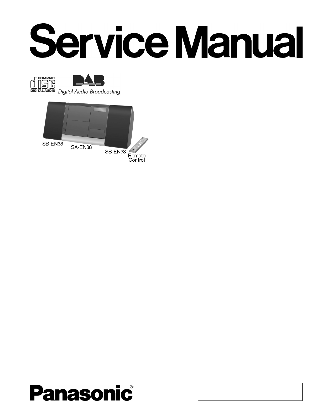
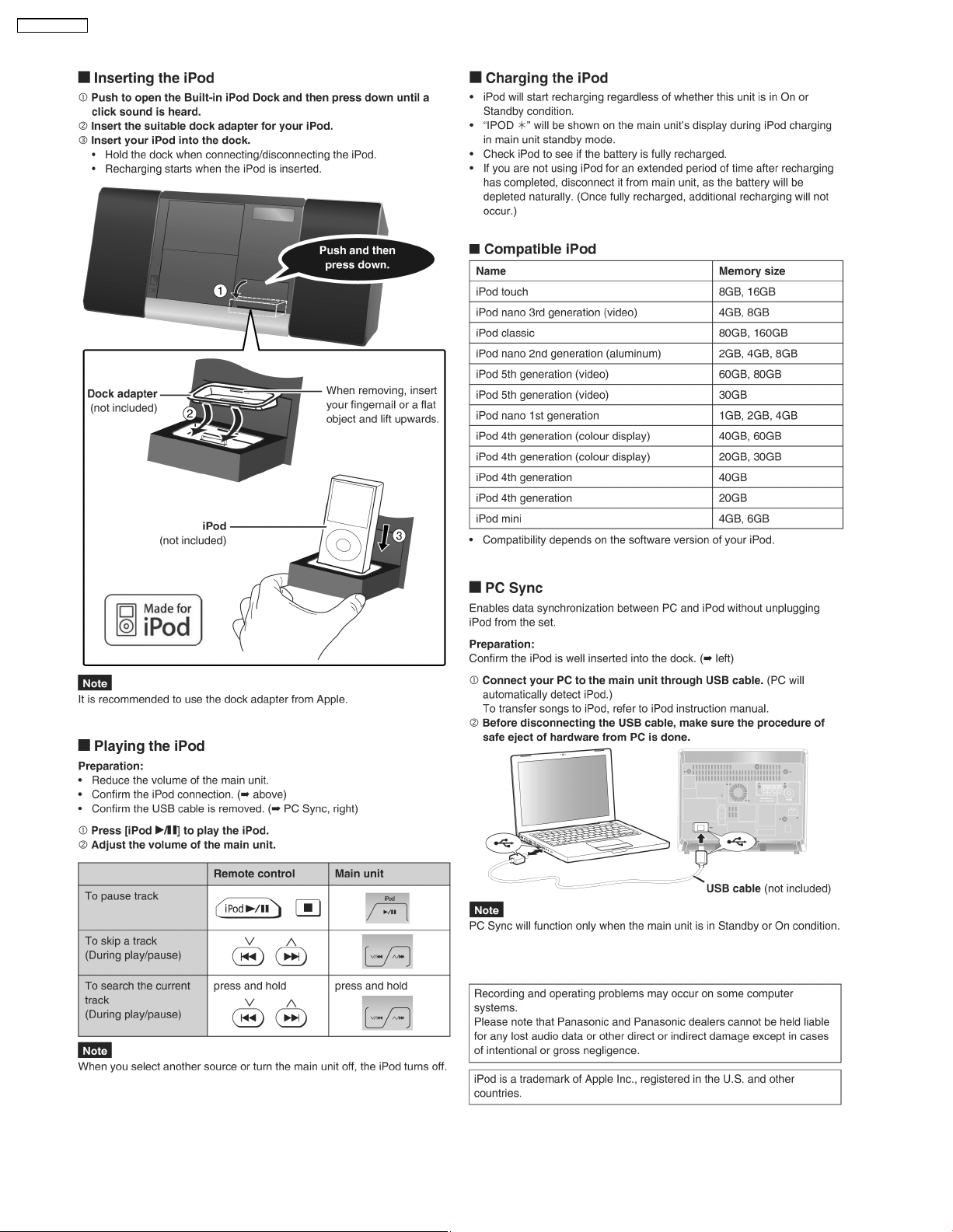
Page 1
I
RMS
10%
1
Input
Sensitivity
Terminal
Output
Terminal
Option
I
FM
Frequency
I
Disc
(1)
(2)
(3)
Sampling
CD
MP3
Bit
MP3
CD Stereo System
SC-EN38DBEB
Colour
(K)... Black Type
ORDER NO. MD0803005CE
Specifications
AMPLIFIER SECTION
OUTPUT POWER both channel driven simultaneously
total harmonic distortion (THD)
kHz 3 W per channel (6 Ω)
Music Port
100 mv, 15 kΩ
Stereo, 3.5 mm jack
Headphone
Stereo, 3.5 mm jack
(16 Ω to 32 Ω)
Port Version 1
TUNER SECTION
range
87.50 MHz to 108.00 MHz (50 kHz)
CD SECTION
played [8cm or 12cm]
CD-Audio (CD-DA)
CD-R/RW (CD-DA, MP3)
MP3
frequency
44.1 kHz
32 kHz, 44.1 kHz, 48 kHz
rate
32 kbps to 384 kbps
Decoding 16/20/24 bit linear
Pick up
Wavelength 785 nm
Laser power CLASS 1
Audio Output (Disc)
Number of channels 2 channel
Audio performance
Frequency response (CD-Audio) 20 Hz to 20 kHz
Wow and flutter Below measurement limit
Digital filter 8
D/A converter MASH (1 bit DAC)
I USB SECTION
Media file format support MP3 (*.mp3)
I DAB SECTION
DAB memories 20 channels
Frequency Band (Waveleng th)
Band III (UK only)
11B to 12D (218.640 MHz to 229.072 MHz)
DAB External Antenna
Terminal F-Connector (75 Ω)
I SPEAKER SECTION
Type 1 Way, 1 speaker system
(Bass reflex)
Speaker (s)
Full range Speaker 7 cm cone type
© 2008 Matsushita Electric Industrial Co. Ltd.. All
rights reserved. Unauthorized copying and
distribution is a violation of law.
Page 2
SC-EN38DBEB
Impedance 6 Ω
Input power (IEC) 3W(MAX)
Dimension (W x H x D) 120 mm x 202.8 mm x 133.5 mm
I GENERAL
Power supply AC 230 to 240 V, 50 Hz
Power consumpti on 30 W
Dimension (W x H X D) 252.5mm x 202.8mm x 133.5 mm
Mass
With speakers Approx. 3.20 kg
Without speakers Approx. 1.90 kg
Operating temperature range 0°Cto+40°C
Operation humidity range 35% to 80% RH (no condensation)
Power consumpti on in standby mode:
Notes:
• Specifications are subject to change without notice.
• Total harmonic distortion is measured by the digital spectrum
analyzer.
I System : SC-EN38DBEBK Main Unit: SA-EN38DBEBK
Speaker: SB-EN38P-K
CONTENTS
Page Page
1 Safety Precautions
2 Prevention of Electro Static Discharge (ESD) to
Electrostatically Sensitive (ES) Devices
3 Precaution of Laser Diode
4 Handling Precautions For Traverse Deck
5 Handling the Lead free Solder
6 Accessories
7 Operation Procedures
8 Self diagnosis and special mode setting
9 Assembling and Disassembling
10 Service Fixture and Tools
3
11 Service Position
12 Voltage Measurement & Waveform Chart
13 Wiring Connection Diagram
6
7
14 Block Diagram
8
15 Notes Of Schematic Diagram
16 Schematic Diagram
9
10
17 Printed Circuit Board
11
18 Illustration of IC’s, Transistors and Diodes
19 Terminal Function of IC’s
16
21
20 Exploded Views
51
21 Replacement Parts List
2.6 W (approx.)
52
60
67
69
75
77
89
95
96
101
105
2
Page 3
SC-EN38DBEB
1 Safety Precautions
1.1. General Guidelines
1. When servicing, observe the original lead dress. If a short circuit is found, replace all parts which have been overheated or
damaged by the short circuit.
2. After servicing, ensure that all the protective devices such as insulation barriers, insulation papers shields are properly installed.
3. After servicing, check for leakage current checks to prevent from being expose d to shock hazards.
1.1.1. Leakage Current Cold Check
1. Unplug the AC cord and connect a jumper between the two prongs on the plug.
2. Using an ohmmeter measure the resistance value, between the jumpered AC plug and each exposed metallic cabinet part on
the equipment such as screwheads, connectors, control shafts, etc. When the exposed metallic part has a return path to the
chassis, the reading should be between 1MΩ and 5.2Ω.
When the exposed metal does not have a return path to the chassis, the reading must be
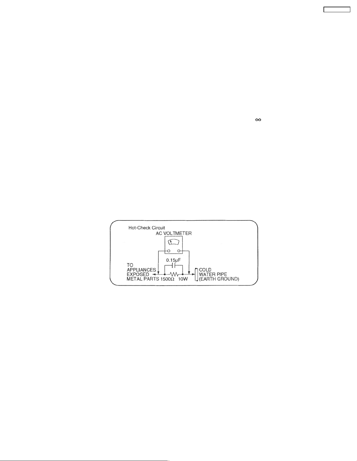
1.1.2. Leakage Current Hot Check
1. Plug the AC cord directly into the AC outlet. Do not use an isolation transformer for this check.
2. Connect a 1.5kΩ, 10 watts resistor, in parallel with a 0.15µF capacitors, between each exposed metallic part on the set and a
good earth ground such as a water pipe, as shown in Figure 1.
3. Use an AC voltmeter, with 1000 ohms/volt or more sensitivity, to measure the potential across the resistor.
4. Check each exposed metallic part, and measure the voltage at each point.
5. Reverse the AC plug in the AC outlet and repeat each of the above measurements.
6. The potential at any point should not exceed 0.75 volts RMS. A leakage current tester (Simpson Model 229 or equivalent) may
be used to make the hot checks, leakage current must not exceed 1/2 milliamp. should the measurement is outside of the limits
specified, there is a possibility of a shock hazard, and the equipment should be repaired and re-checked before it is returned
to the customer.
.
Fig. 1
3
Page 4
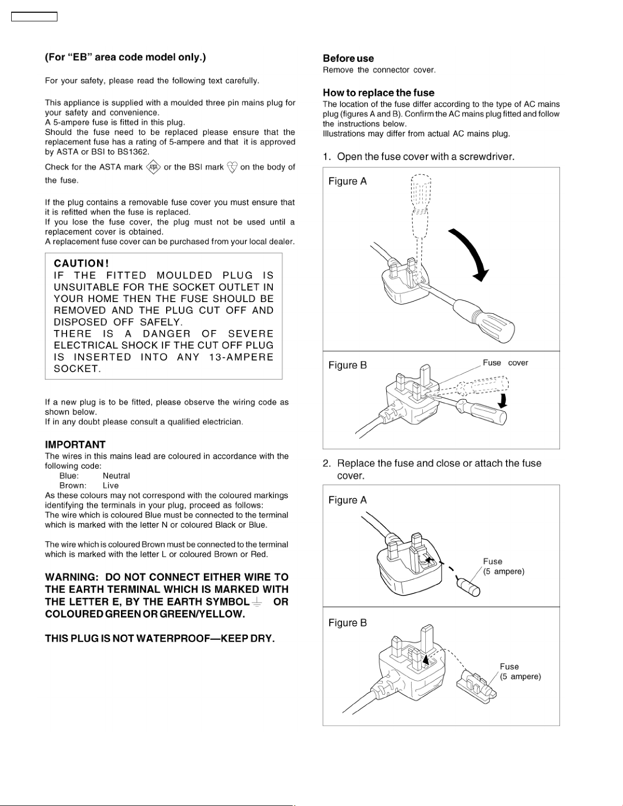
SC-EN38DBEB
1.2. Caution for AC Cord
4
Page 5
SC-EN38DBEB
1.3. Before Repair and Adjustment
Disconnect AC power, discharge Power Supply Capacitors C501 through a 10Ω, 1W resistor to ground.
DO NOT SHORT-CIRCUIT DIRECTLY (with a screwdriver blade, for instance), as this may destroy solid state devices.
After repairs are completed, restore power gradually using a variac, to avoid overcurrent.
• Current consumption at AC 230-240 V, 50 Hz in NO SIGNAL mode should be ~300 mA.
1.4. Protection Circuitry
The protection circuitry may have operated if either of the following conditions are noticed:
• No sound is heard when the power is turned on.
• Sound stops during a performance.
The function of this circuitry is to prevent circuitry damage if, for example, the positive and negative speaker connection wires are
"shorted", or if speaker systems with an impedance less than the indicated rated impedance of the amplifier are used.
If this occurs, follow the procedure outlines below:
1. Turn off the power.
2. Determine the cause of the problem and correct it.
3. Turn on the power once again after one minute.
Note:
When the protection circuitry functions, the unit will not operate unless the power is first turned off and then on again.
1.5. Safety Part Information
Safety Parts List:
There are special components used in this equipment which are important for safety.These parts are marked by
Schematic Diagrams & Replac ement Parts List. It is essential that these critical parts should be replaced with manufacturer’s
specified parts to prevent shock, fire or other hazards. Do not modify the original design without permission of manufacturer.
Table 1
Reference No. Part No. Part Name & Description Remarks
A2 K2CT3CA00004 AC CORD [M]
JK600 K2AA2B000017 AC INLET [M]
T600 G4CYAYY00176 TRANSFORMER [M]
F1 K5D202BLA013 FUSE [M]
L600 ELF15N035AN LINE FILTER [M]
301 RAE0165T-V TRAVERSE (W/O CD SERVO P. C. B.) [M] (RTL)
FP841 K5G251A00008 FUSE PROTECT OR [M]
FP600 K5G302AA0002 FUSE PROTECTOR [M]
R260 ERD2FCVG470T RESISTOR [M]
PCB6 REPX0652A TRANSFORMER P.C.B. [M] (RTL)
PCB7 REPX0652C AC INLET P.C.B [M] (RTL)
in the
5
Page 6

SC-EN38DBEB
2 Prevention of Electro Static Discharge (ESD) to
Electrostatically Sensitive (ES) Devices
Some semiconductor (solid state) devices can be damaged easily by electricity. Such components commonly are called
Electrostatically Sensitive (ES) Devices. Examples of typical ES devices are integrated circuits and some field-effect transistors and
semiconductor “chip” components. The following techniques should be used to help reduce the inciden ce of component damage
caused by electro static discharge (ESD).
1. Immediately before handlin g any semiconductor component or semiconductor-equiped assembly, drain off any ESD on your
body by touchin g a known earth ground. Alternatively, obtain and wear a commercially available discharging ESD wrist strap,
which should be removed for potential shock reasons prior to applyin g power to the unit under test.
2. After removing an electrical assembly equiped with ES devices, place the assembly on a conductive surface such as aluminium
foil, to prevent electrostatic charge build up or exposure of the assembly.
3. Use only a grounded-tip soldering iron to solder or unsolder ES devices.
4. Use only an anti-static solder remover device. Some solder removal devices not classified as “anti-static (ESD protected)” can
generate electrical charge to damage ES devices.
5. Do not use freon-propelled chemicals. These can generate electrical charges sufficient to damage ES devices.
6. Do not remove a replacement ES device from its protective package until immediately before you are ready to install it. (Most
replacement ES devices are packaged with leads electrically shorted together by conductive foam, aluminium foil or
comparable conductive material).
7. Immediately before removing the protective material from the leads of a replacement ES device, touch the protective material
to the chassis or circuit assembly into which the device will be installed.
Caution
Be sure no power is applied to the chassis or circuit, and observe all other safety precautions.
8. Minimize body motions when handlin g unpackaged replacement ES devices. (Otherwise harmless motion such as the brushing
together of your clothes fabric or the lifting of your foot from a carpeted floor can generate static electricity (ESD) sufficient to
damage an ES device).
6
Page 7
SC-EN38DBEB
3 Precaution of Laser Diode
CAUTION:
This unit utilizes a class 1 laser (Wavelength: 785 nm).
Invisible laser radiation is emitted from the optical pickup lens.
When the unit is turned on:
1. Do not look directly into the pick up lens.
2. Do not use optical instruments to look at the pick up lens.
3. Do not adjust the preset variable resistor on the pickup lens.
4. Do not disassemble the optical pick up unit.
5. If the optical pick up is replaced, use the manufacturer’s specified replacement pick up only.
6. Use of control or adjustments or performance of procedures other than those specified herein may result in hazardous radiation
exposure.
CAUTION!
THIS PRODUCT UTILIZES A LASER.
USE OF CONTROLS OR ADJUSTMENTS OR PERFORMANCE OF PROCEDURES OTHER THAN THOSE SPECIFIED HEREIN MAY RESULT
IN HAZARDOUS RADIATION EXPOSURE.
7
Page 8
SC-EN38DBEB
4 Handling Precautions For Traverse Deck
The laser diode in the traverse deck (optical pickup) may break
down due to potential difference caused by static electricity of
clothes or human body.
So, be careful of electrostatic breakdown during repair of the
traverse deck (optical pickup).
G Handling of CD traverse deck (optical pickup)
1. Do not subject the traverse deck (optical pickup) to
static electricity as it is extremely sensitive to electrical
shock.
2. The short land between the No.4 (LD) and No.5 (GND)
pins on the flexible board (FFC) is shorted with a solder
build-up to prevent damage to the laser diode.
3. Take care not to apply excessive stress to the flexible
board (FFC board) (Fig 4.1).
4. Do not turn the variable resistor (laser power
adjustment). It has already been adjusted.
Fig 4.2
Fig 4.1
G Grounding for electrostatic breakdown prevention
1. Human body grounding ()
Use the anti-static wrist strap to discharge the static
electricity from your body.
2. Work table grounding ()
Put a conduc tive material (sheet) or steel sheet on the
area where the traverse deck (optical pickup) is placed,
and ground the sheet.
Caution :
The static electricity of your clothes will not be grounded
through the wrist strap. So, take care not to let your
clothes touch the traverse deck (optical pickup).
Caution when Replacing the Optical Pickup :
The traverse has a short point shorted with solder to protect
the laser diode against electrostatics breakdown. Be sure to
remove the solder from the short point before making
connections.
8
Page 9
SC-EN38DBEB
5 Handling the Lead free Solder
5.1. General description about Lead Free Solder (PbF)
The lead free solder has been used in the mounting process of all electrical components on the printed circuit boards used for this
equipment in considering the globally environmental conservation.
The normal solder is the alloy of tin (Sn) and lead (Pb). On the other hand, the lead free solder is the alloy mainly consists of tin
(Sn), silver (Ag) and Copper (Cu), and the melting point of the lead free solder is higher approx.30 degrees C (86°F) more than that
of the normal solder.
Definition of PCB Lead Free Solder being used
The letter of “PbF” is printed either foil side or components side on the PCB using the lead free solder.
(See right figure)
Service caution for repair work using Lead Free Solder (PbF)
• The lead free solder has to be used when repairing the equipment for which the lead free solder is used.
(Definition: The letter of “PbF” is printed on the PCB using the lead free solder.)
• To put lead free solder, it should be well molten and mixed with the original lead free solder.
• Remove the remaining lead free solder on the PCB cleanly for soldering of the new IC.
• Since the melting point of the lead free solder is higher than that of the normal lead solder, it takes the longer time to melt
the lead free solder.
• Use the soldering iron (more than 70W) equipped with the temperature control after setting the temperature at 350±30
degrees C (662±86°F).
Recommended Lead Free Solder (Service Parts Route.)
• The following 3 types of lead free solder are available through the service parts route.
RFKZ03D01K-----------(0.3mm 100g Reel)
RFKZ06D01K-----------(0.6mm 100g Reel)
RFKZ10D01K-----------(1.0mm 100g Reel)
Note
* Ingredient: Tin (Sn), 96.5%, Silver (Ag) 3.0%, Copper (Cu) 0.5%, Cobalt (Co) / Germanium (Ge) 0.1 to 0.3%
9
Page 10
SC-EN38DBEB
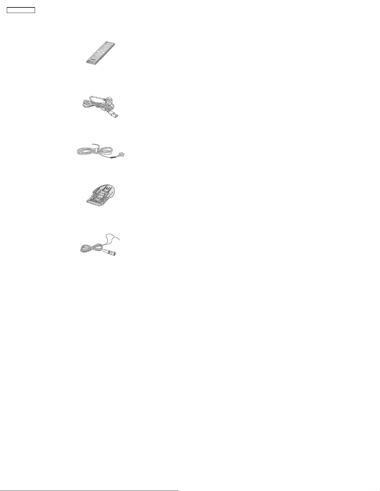
6 Accessories
Note : Refer to Packing Materials & Accessories (Section 21) for part number.
Remote
control
AC cord
AM antenna
Support stand
DAB antenna
10
Page 11
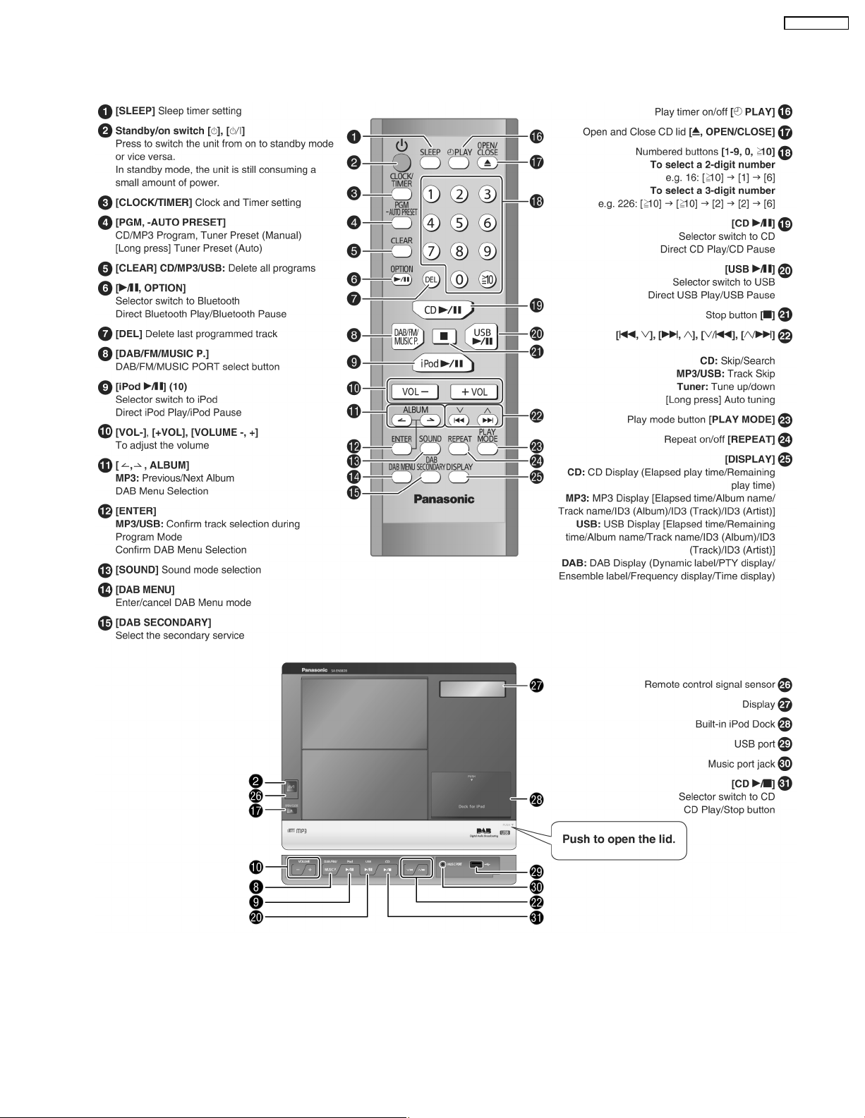
7 Operation Procedures
7.1. Main Unit & Remote Control Key Buttons Operation
SC-EN38DBEB
11
Page 12
SC-EN38DBEB
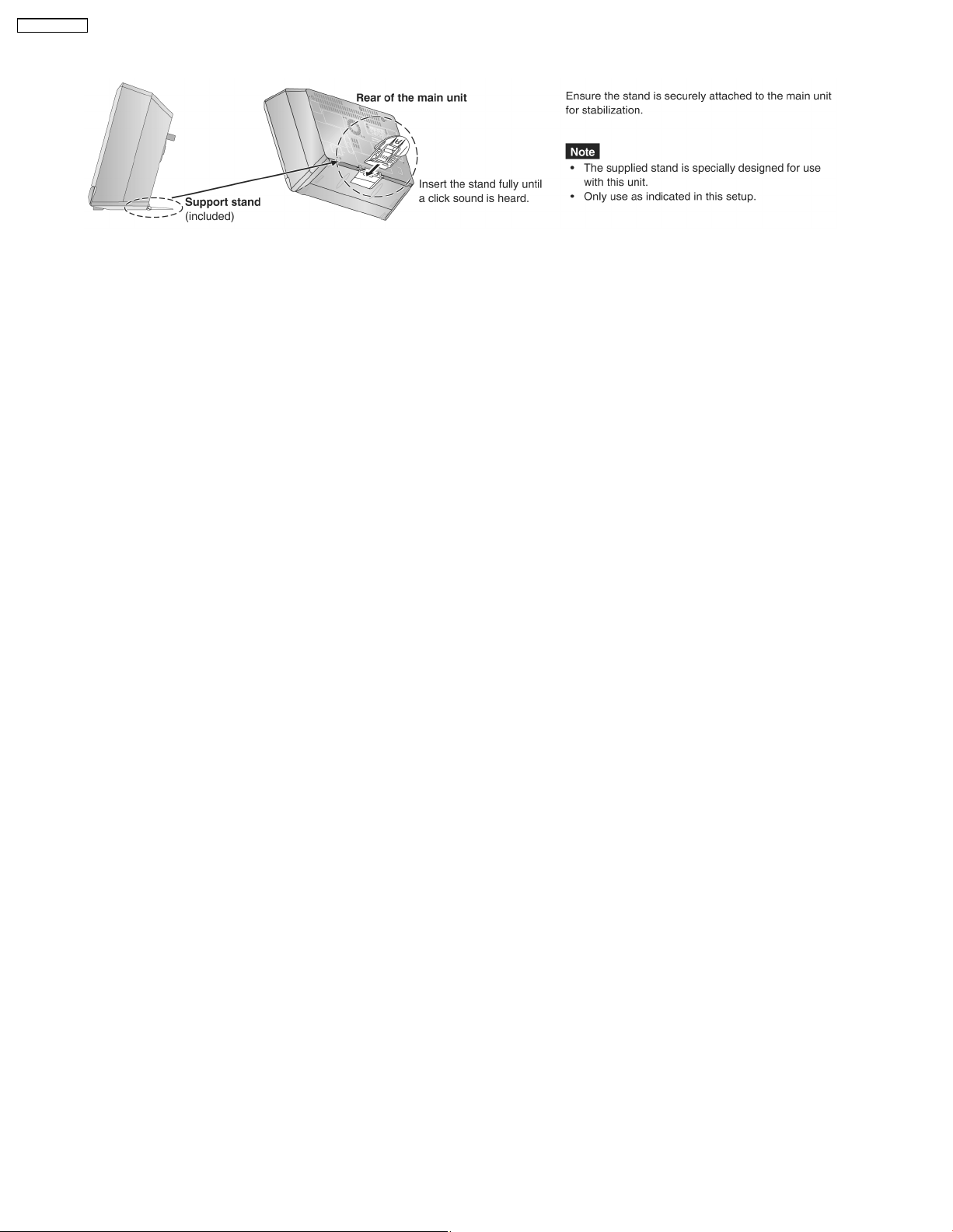
7.2. Attach the stand to the unit
12
Page 13
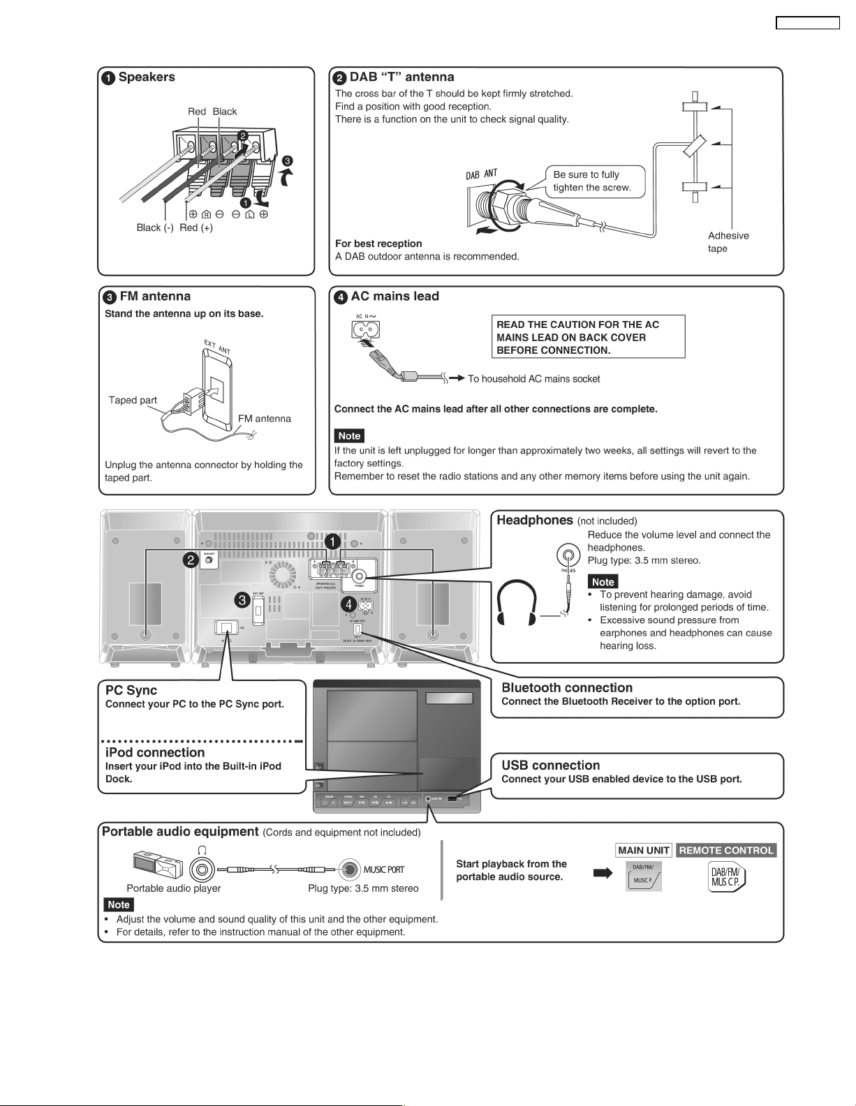
7.3. Connection
SC-EN38DBEB
13
Page 14
SC-EN38DBEB
7.4. External unit
14
Page 15
7.5. Disc Information
SC-EN38DBEB
15
Page 16
SC-EN38DBEB
8 Self diagnosis and special mode setting
This unit is equipped with features of self-diagnostic & special mode setting for checking the functions & reliability.
8.1. Service Mode Summary Table
The service mode can be activated by pressing various button combination on the main unit and remote control unit. Below is the
summary for the various modes for checking:-
Player buttons Remote control unit buttons Application Note
[Volume -] [4], [7] To enter into doctor mode for various item
checking.
Mode Remote control unit buttons Application Note
Doctor Mode [2] FL ALL Segment inspection (Refer to the section 8.2 for more
[7], [8], [9] Forced VOL setting (Refer to the section 8.2 for more
[ ], [1], [1] CD Loading Test (Refer to the section 8.2 for more
[ ], [1], [2] CD Traverse Test (Refer to the section 8.2 for more
[ ], [1], [3] CD Combination Test (Refer to the section 8.2 for more
[ ], [1], [4] CD Auto Adjustment Display (Refer to the section 8.2 for more
[SLEEP] Cold Start setting (Refer to the section 8.2 for more
[2] USB TEST (Refer to the section 8.2 for more
(Refer to the section 8.2 for more
information.)
information.)
information.)
information.)
information.)
information.)
information.)
information.)
information.)
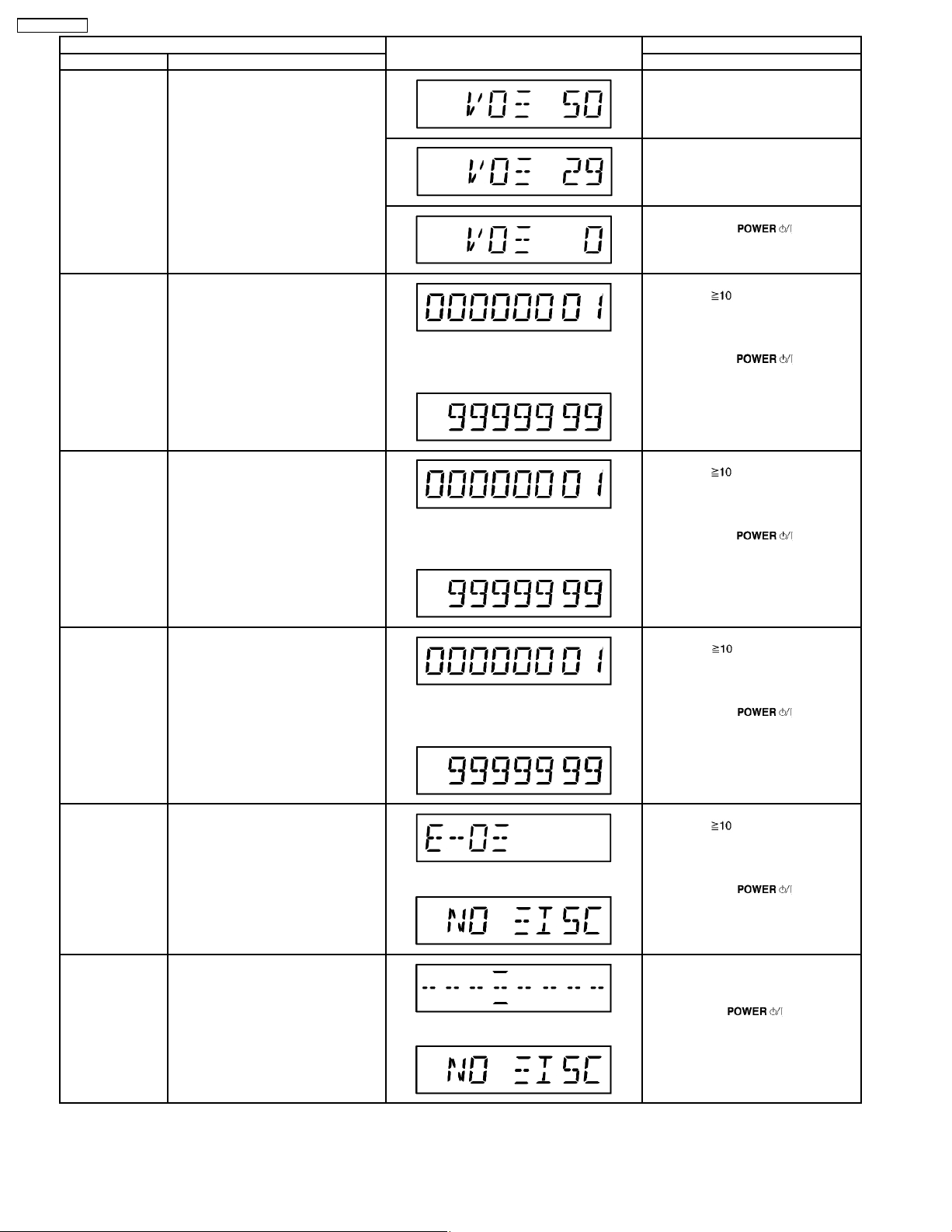
8.2. Service Mode Table 1
Below is the various special modes for checking:-
Item FL Display Key Operation
Mode Name Description Front Key
Self-Diagnostic
Mode
To enter into self diagnostic checking
for main unit.
1. Select [CD] for CD mode (Ensure
no CD inserted.)
2. Press and hold [Volume -] button
for 2 seconds follow by [FF]
To exit, press [
main unit or remote control.
] button on
16
Page 17
Item FL Display Key Operation
Mode Name Description Front Key
Doctor Mode To enter into Doctor Mode for
checking of various items and
displaying EEPROM and firmware
version.
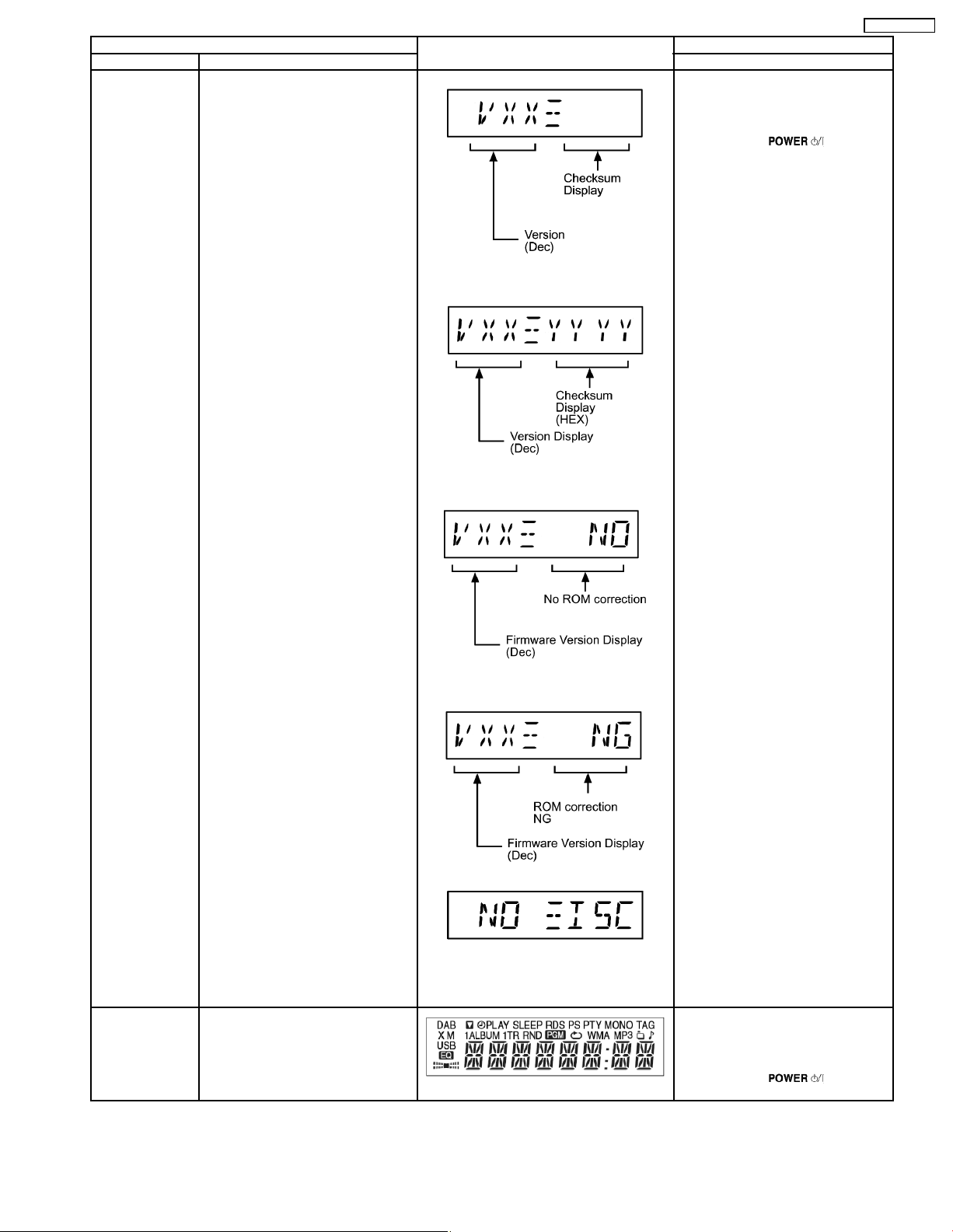
Note: The micro-processor version as
shown is an example. It will be revise
when there is an updates.
DIsplay 1
In any mode:
1. Press [Volume -] button on main
unit follow by [4] and [7] on remote
control.
To exit, press [
main unit or remote control.
FL Display sequence
Display 1 → 2
Checksum (Condition 1)
When EEPROM IC detected and has ROM
correction.
Checksum (Condition 2)
When EEPROM IC is detected and there is
no ROM correction.
SC-EN38DBEB
] button on
FL Display Test To check the FL segments display (All
segments will light up)
Checksum (Condition 3)
When EEPROM IC is detected and has ROM
correction but not working properly.
Display 2
The Check Sum of EEPROM and firmware
version will be display for 1 sec.
* ROM correction
** Firmware version No:
In doctor mode:
1. Press [2] button on remote control.
To cancel, press [0] button remote
control.
To exit, press [
] button on
main unit or remote control.
17
Page 18
SC-EN38DBEB
Volume Setting
Mode
Item FL Display Key Operation
Mode Name Description Front Key
To check for the volume setting of the
main unit. The volume will be
In doctor mode:
1. Press [7] button on remote control.
automatically set to its respective
level (in dB). During the mode,
treble/bass/EQ will be set to “0” dB &
OFF.
2. Press [8] button on remote control.
CD Loading Test
Mode
CD Traverse Unit
Test Mode
CD Combination
Test Mode
To determine the reliability of CD
Loading unit.
To check for the Open/Close
operation for the CD loading unit. It
fails when there is abnormality in
opening or closing.
To check for the traverse unit
operation. In this mode, the first & last
track is access & read. (TOC). It fails
when TOC is not completed by IOS or
the traverse is out of focus.
A combination of CD loading &
traverse unit test.
The counter will increment by 1 until reach
9999999
↓
The counter will increment by 1 until reach
9999999
↓
The counter will increment by 1 until reach
9999999
↓
3. Press [9] button on remote control.
To exit, press [
] button on
main unit or remote control.
In doctor mode:
1. Press [
], [1] & [1] button on
remote control.
To cancel, press [0] button remote
control.
To exit, press [
] button on
main unit or remote control.
In doctor mode:
1. Press [
], [1] & [2] button on
remote control.
To cancel, press [0] button remote
control.
To exit, press [
] button on
main unit or remote control.
In doctor mode:
1. Press [
], [1] & [3] button on
remote control.
To cancel, press [0] button remote
control.
To exit, press [
] button on
main unit or remote control.
CD Auto
Adjustment
Display
To display result of self adjustment for
CD.
For more information, please refer to
Section 8.2.1.
Cold Start To activate cold start upon next AC
power up.
The [NO DISC] display will appear after 3s,
The [NO DISC] display will appear after 3s,
18
In doctor mode:
1. Press [
], [1] & [4] button on
remote control.
To cancel, press [0] button remote
control.
To exit, press [
] button on
main unit or remote control.
In doctor mode:
1. Press [SLEEP] button on remote
control.
To exit, press [
] button on
main unit or remote control.
Page 19
Item FL Display Key Operation
Mode Name Description Front Key
USB Test Mode To Inspect USB Testing.
The display will appear after 3s,
In doctor mode:
1. Select [USB
2. Press [2] button on remote control.
To exit, press [
main unit or remote control.
] for USB mode.
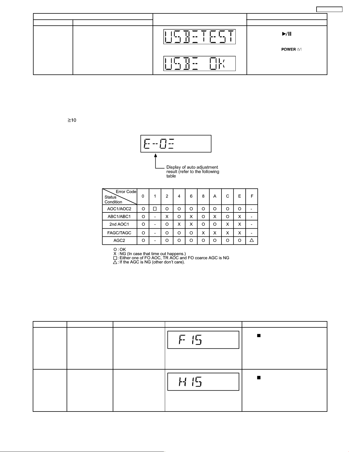
8.2.1. CD Self-Adjustment (AJST) Result Display
Purpose: To display result of self-adjustment for CD.
Below is the procedures for this mode.
Step 1: Enter into Doctor mode (For more information refer to section 8.2 on key operation to enter into this mode).
Step 2: When [
to the condition met as shown in the table below:
], [1] & [4] are pressed at the doctor mode, the following shall be display ed for 3s. The result shall correspond
SC-EN38DBEB
] button on
8.3. Error Code Table 1
8.3.1. Mechanism Error Code Table
Self-Diagnosis Function provides information on any problems occuring for the unit and its respective components by displaying
error codes. These error code such as U**, H** and F** are stored in memory and held unless it is cleared.
The error code is automatically display after entering into self-diagnostic mode.
Error Code Diagnosis Contents Description of error Automatic FL Display Remarks
F15 CD REST SW
abnormal
H15 CD OPEN SW
abnormal
CD traverse position
initial setting operation
fail-safe counter
(1000ms) waiting for
REST SW to turn on.
Error no. shall be clear
by force or during cold
start.
During normal operation,
if CD OPEN SW ON is
not detected within 4
sec, and then H15 shall
be memorized. The error
code can be cleared only
at the start up of micro-p
after reset.
19
For CD unit.(For traverse).
Press [
For CD unit.(For traverse).
Press [
] on main unit for next error.
] on main unit for next error.
Page 20
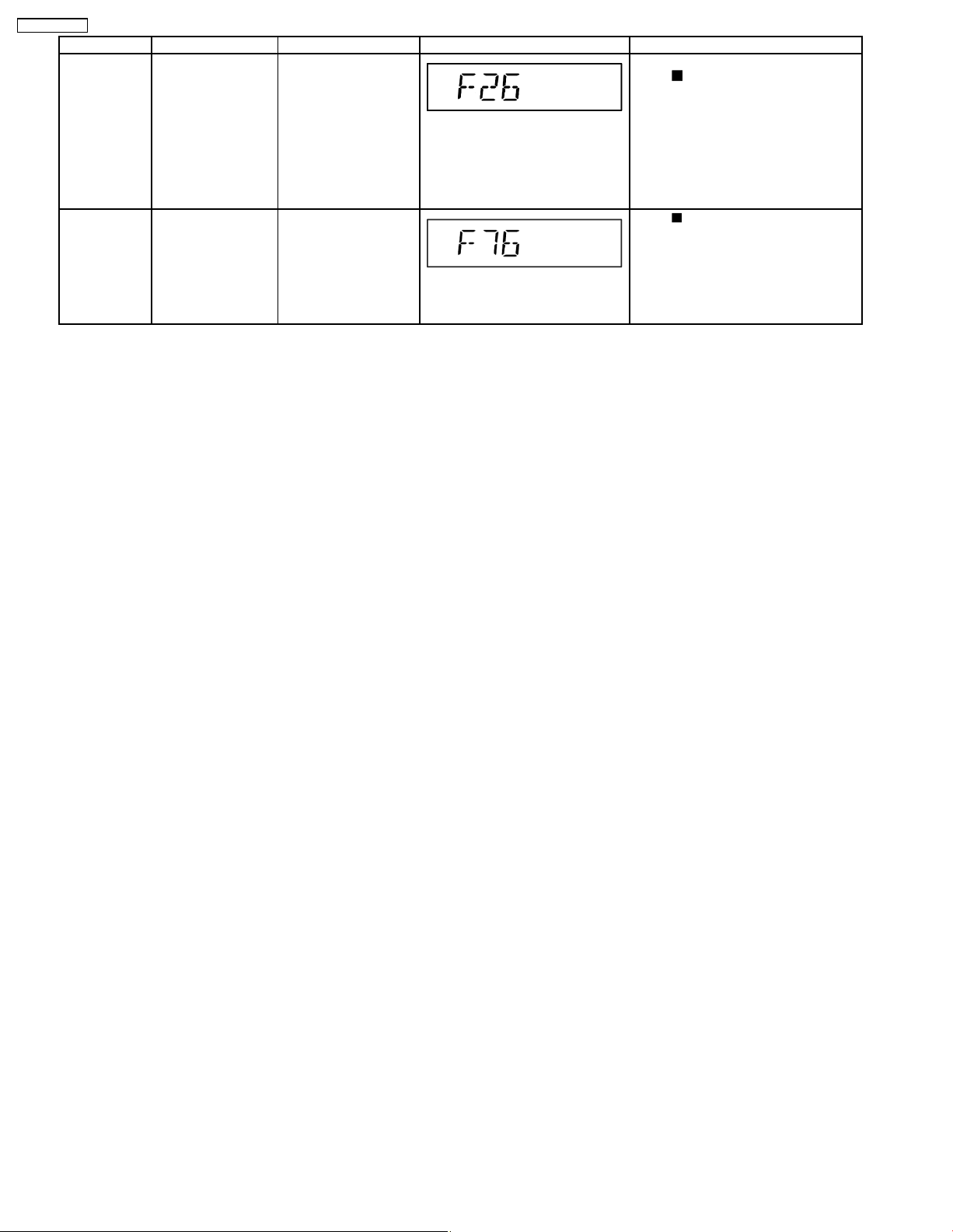
SC-EN38DBEB
Error Code Diagnosis Contents Description of error Automatic FL Display Remarks
F26 Communication
between CD servo
LSI and micro-p
abnormal.
F76 Abnormality in the
output voltage of
stabilized power
supply.
CD function DTMS
command, after system
setting, if SENSE = “L”
cannot be detected.
Memory shall contain
F26code. After power
on, CD function shall
continue, error display
shall be “NO DISC”.
Error no. shall be clear
by force or cold start.
In normal operation
when “DCDET” is
detected “L” (IOIO) for
two consecutive times,
this error code will be
displayed for 2s & after
PCONT will be turned to
“L” (Low).
For CD unit.(For traverse).
Press [
] on main unit for next error.
Press [ ] on main unit for next error.
20
Page 21
SC-EN38DBEB
9 Assembling and Disassembling
9.1. Caution
“ATTENTION SERVICER”
Be careful when disassembling and servicing.
Some chassis components may have sharp edges.
Special Note:
1. This section describes the disassembly procedures for all the major printed circuit boards and main components.
2. Before the disassembly process was carried out, do take special note that all safety precautions are to be carried out.
(Ensure that no AC power supply is connected during disassembling.)
3. For assembly after operation checks or replacement, reverse the respective procedures.
Special reassembly procedures are described only when required.
4. Do take note of the locators on each printed circuit board during reassembling procedures.
5. The Switch Regulator IC may have high temperature after prolonged use.
6. Use caution when removing the top cabinet and avoid touching heat sinks located in the unit.
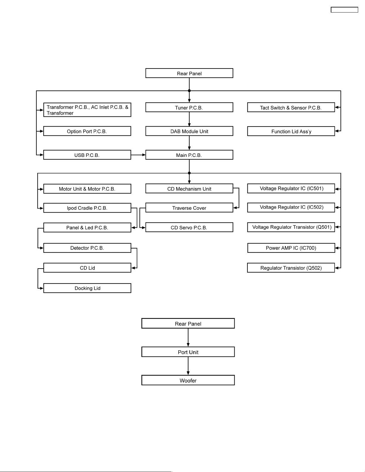
7. Select items from the following index when checks or replacement are required.
• Disassembly of Rear Panel
• Disassembly of Transformer P.C.B., AC Inlet P.C.B. & Transformer
• Disassembly of Option Port P.C.B.
• Disassembly of USB P.C.B.
• Disassembly of Tuner P.C.B.
• Disassembly of DAB Module Unit
• Disassembly of Main P.C.B.
• Replacement of Voltage Regulator IC (IC501)
• Replacement of Voltage Regulator IC (IC502)
• Replacement of Voltage Regulator Transistor (Q501)
• Replacement of Power AMP IC (IC700)
• Replacement of Regulator Transistor (Q502)
• Disassembly of Tact Switch & Sensor P.C.B.
• Disassembly of CD Mechanism Unit
• Disassembly of Traverse Cover
• Disassembly of CD Servo P.C.B.
• Disassembly of Motor Unit & Motor P.C.B.
• Disassembly of Ipod Cradle P.C.B.
• Disassembly of Panel & LED P.C.B.
• Disassembly of Detector P.C.B.
• Disassembly of CD Lid
• Disassembly of Docking Lid
• Disassembly of Function Lid Ass’y
• Disassembly of Speaker
21
Page 22

SC-EN38DBEB
22
Page 23
SC-EN38DBEB
9.2. Disassembly flow chart
The following chart is the procedure for disassembling the casing and inside parts for internal inspection when carrying out the
servicing.
To assemble the unit, reverse the steps shown in the chart below.
9.2.1. For Main unit
9.2.2. For Speaker unit (SB-EN38)
23
Page 24
SC-EN38DBEB
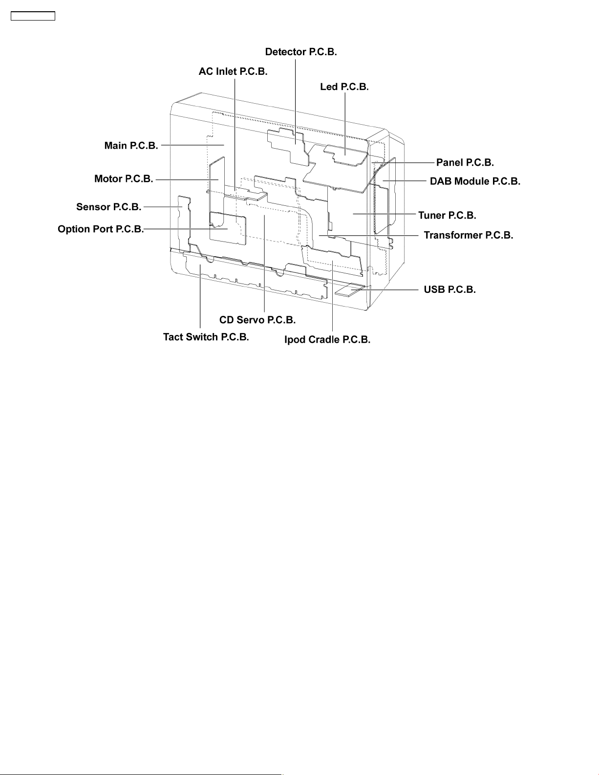
9.3. Main Parts Location Diagram
24
Page 25
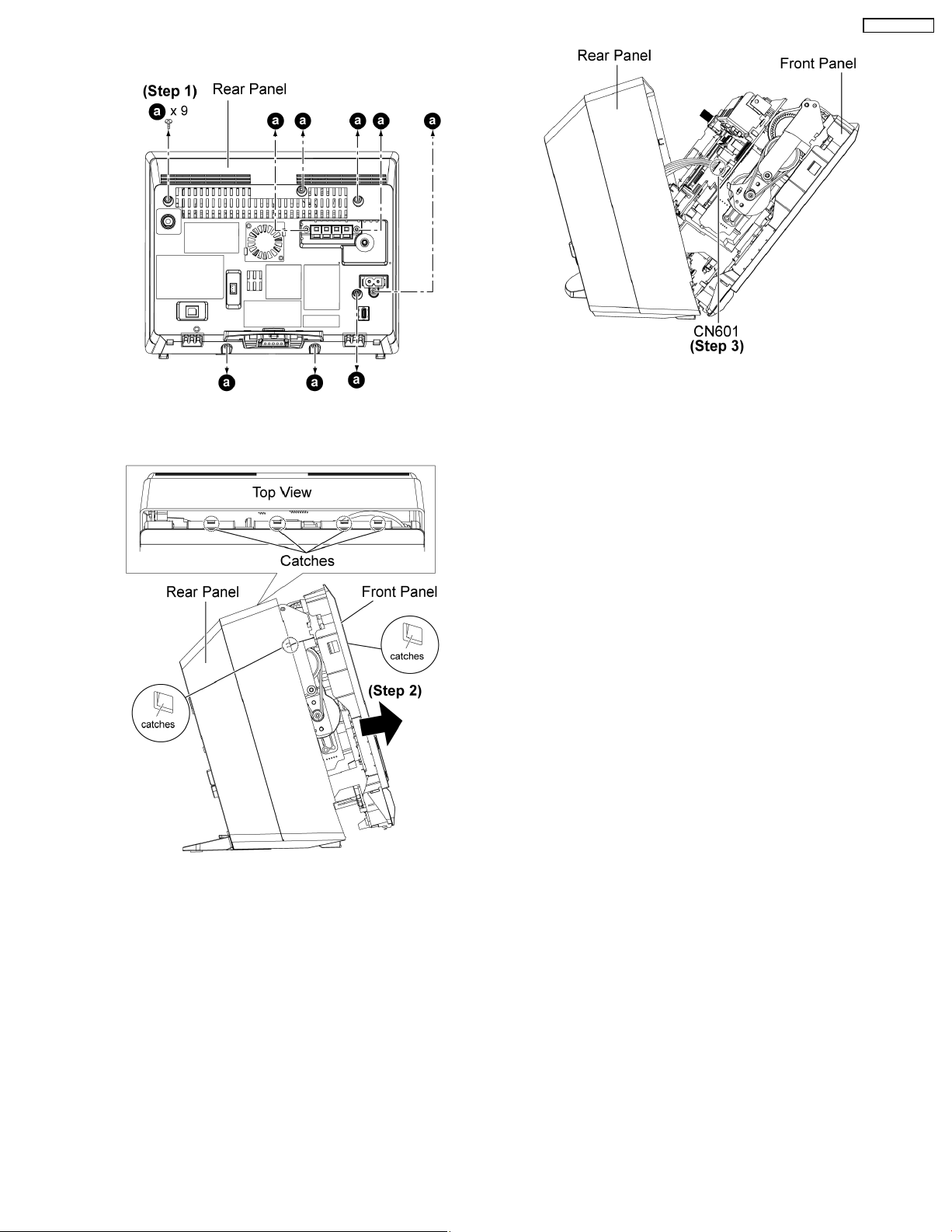
9.4. Disassembly of Rear Panel
Step 1 : Remove 9 screws.
SC-EN38DBEB
Step 3 : Detach 3P cable at connector (CN601) on Main P.C.B.
and remove Rear Panel.
Step 2 : Release 6 catches and slightly push the Rear Panel as
arrow shown.
25
Page 26
SC-EN38DBEB
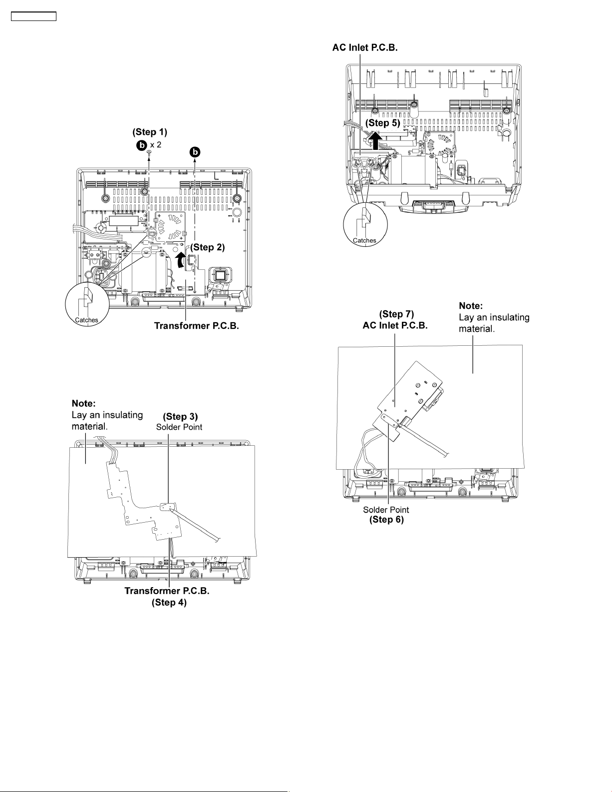
9.5. Disassembly of Transformer
P.C.B., AC Inlet P.C.B. &
Transformer
• Follow the (Step 1) - (Step 3) of item 9.4.
• Disassembly of Transformer P.C.B.
• Disassembly of AC Inlet P.C.B.
Step 5 : Release 2 catches and remove AC Inlet P.C.B. as
arrow shown.
Step 1 : Remove 2 screws.
Step 2 : Release 2 catches and remove Transformer P.C.B. as
arrow show.
Step 3 : Desolder 2 solder point from Transformer P.C.B..
Step 4 : Remove Transformer P.C.B..
Step 6 : Desolder 2 solder point from AC Inlet P.C.B..
Step 7 : Remove AC Inlet P.C.B..
26
Page 27
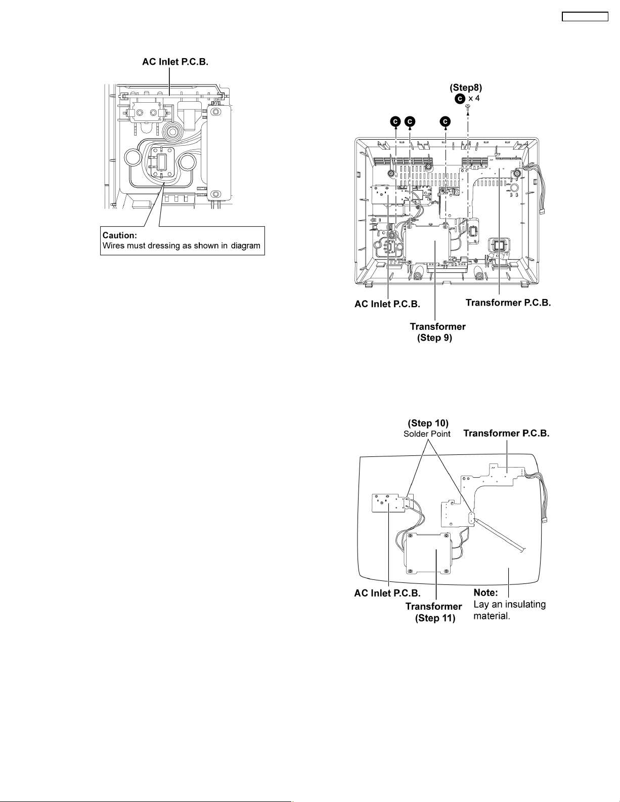
Caution : During reasse mbling procedures, ensure the
cable are properly dressed.
SC-EN38DBEB
• Disassembly of Transformer
− Follow the (Step 1) - (Step 2) of (Disassembly of
Transformer P.C.B.)
− Follow the (Step 5) of (Disassembly of AC Inlet P.C.B.)
Step 8 : Remove 4 screws.
Step 9 : Remove Transformer with AC Inlet & Transformer
P.C.B..
Step 10 : Desolder 4 solder point.
Step 11 : Remove Transformer.
27
Page 28
SC-EN38DBEB
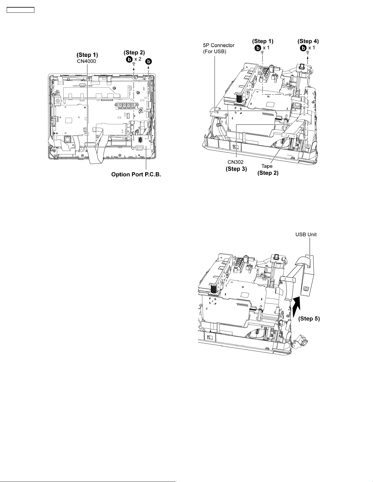
9.6. Disassembly of Option Port
P.C.B.
• Follow the (Step 1) - (Step 3) of item 9.4.
9.7. Disassembly of USB P.C.B.
• Follow the (Step 1) - (Step 3) of item 9.4.
Step 1 : Detach 14P FFC cable at connector (CN4000) on
Option Port P.C.B..
Step 2 : Remove 2 screws.
Step 1 : Remove 1 screw and 5P Connector (For USB).
Step 2 : Remove Tape.
Step 3 : Detach 22P FFC cable at connector (CN302) on Main
P.C.B..
Step 4 : Remove 1 screw.
Step 5 : Remove USB Unit.
28
Page 29
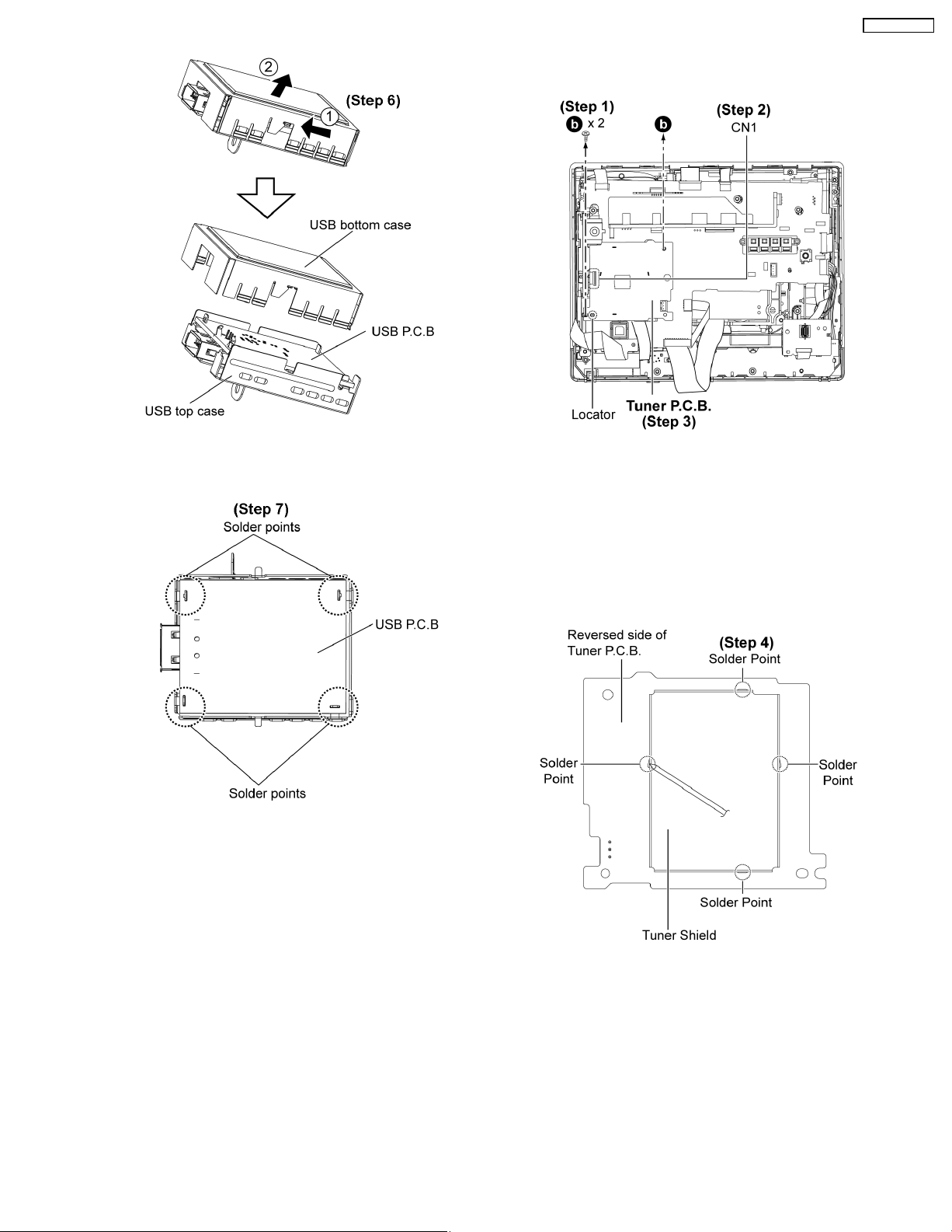
9.8. Disassembly of Tuner P.C.B.
• Follow the (Step 1) - (Step 3) of item 9.4.
SC-EN38DBEB
Step 6 : Remove USB bottom case as arrow shown.
Step 7 : Unsolder the solder point to remove USB P.C.B..
Step 1 : Remove 2 screws.
Step 2 : Detach 12P FFC cable at connector (CN1) on Tuner
P.C.B..
Step 3 : Remove Tuner P.C.B..
Caution : Take extra care for the locator on the Tuner
P.C.B. during removal and assembly of the Tuner P.C.B..
• Disassembly of Tuner Shield
Step 4 : Desolder 4 solder point from Tuner P.C.B. to remove
Tuner Shield.
29
Page 30
SC-EN38DBEB
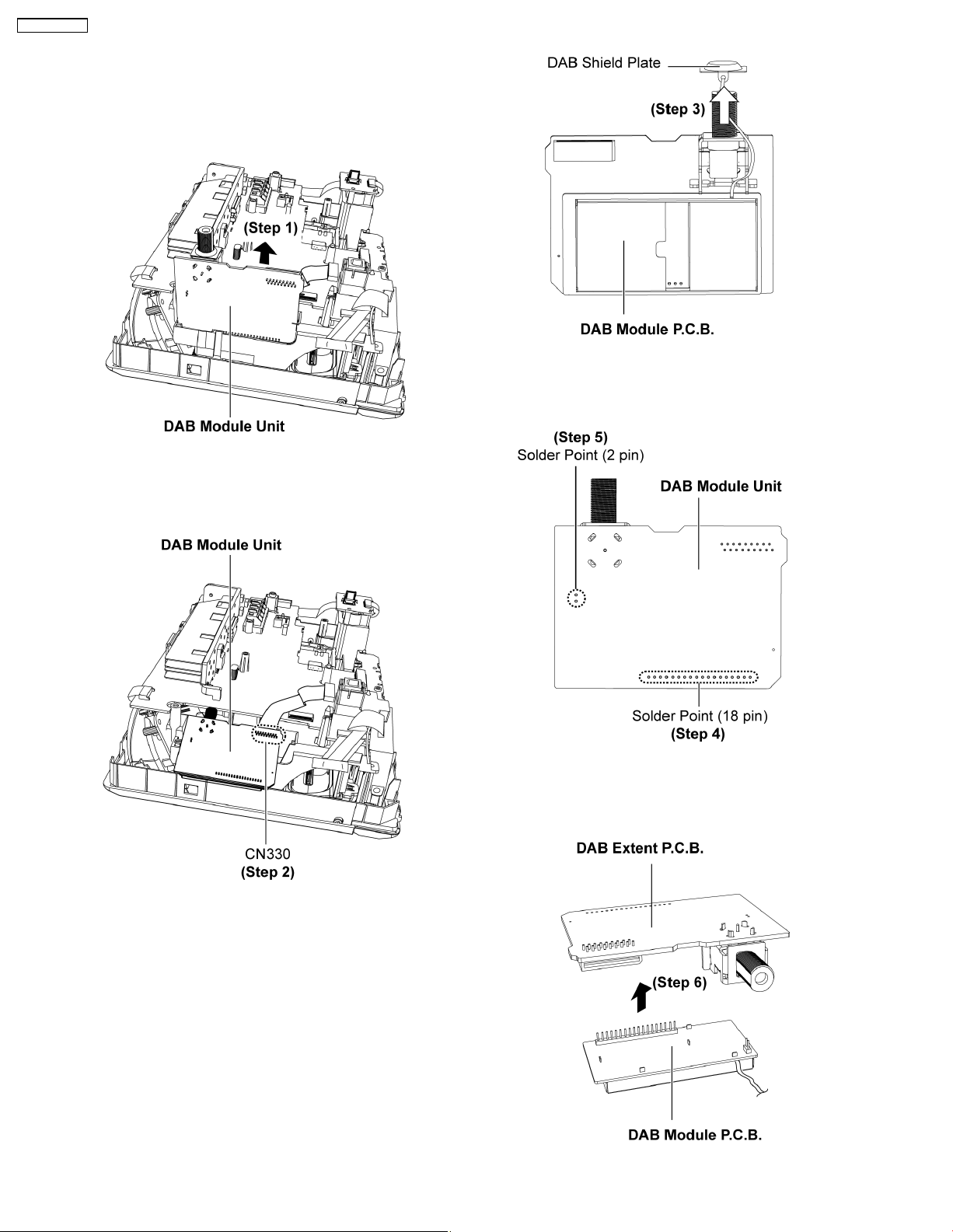
9.9. Disassembly of DAB Module
Unit
• Follow the (Step 1) - (Step 3) of item 9.4.
• Follow the (Step 1) - (Step 3) of item 9.8.
Step 3 : Remove DAB Shield Plate as arrow shown.
Step 1 : Remove DAB Module unit as arrow shown.
Step 2 : Detach 18P FFC cable at connector (CN330) on DAB
Module unit.
Step 4 : Desolder 18P (P1).
Step 5 : Desolder 2P (P201).
30
Page 31

Step 6 : Remove DAB Extent P.C.B. as arrow shown.
Step 7 : Desolder 5 solder point.
SC-EN38DBEB
9.10. Disassembly of Main P.C.B.
• Follow the (Step 1) - (Step 3) of item 9.4.
• Follow the (Step 1) - (Step 3) of item 9.8.
• Follow the (Step 1) - (Step 2) of item 9.9.
Step 8 : Remove shield plate as arrow shown.
Step 1 : Remove 1 screw and 5P connector (For USB).
Step 2 : Detach 14P FFC cable at connector (CN381) on Main
P.C.B..
Step 3 : Detach 22P FFC cable at connector (CN301) on Main
P.C.B..
Step 4 : Detach 8P FFC cable at connector (CN952) on Main
P.C.B..
Step 5 : Detach 8P cable at connector (P900) on Main P.C.B..
Step 6 : Detach 3P cable at connector (P651) on Main P.C.B..
Step 7 : Detach 5P cable at connector (P650) on Main P.C.B..
Step 8 : Detach 14P FFC cable at connector (CN380) on Main
P.C.B..
31
Page 32

SC-EN38DBEB
Step 9 : Detach 22P FFC cable at connector (CN302) on Main
P.C.B..
Step 10 : Remove Main P.C.B..
Caution : Take extra care for the locator on the Main P.C.B.
during removal and assembly of the Main P.C.B..
9.11. Replacement of Voltage
Regulator IC (IC501)
• Follow the (Step 1) - (Step 3) of item 9.4.
• Follow the (Step 1) - (Step 3) of item 9.8.
• Follow the (Step 1) - (Step 2) of item 9.9.
• Follow the (Step 1) - (Step 10) of item 9.10.
Step 1 : Remove 1 screw.
Step 2 : Desold er pins of Voltage Regulator IC (IC501) on the
reverse side of Main P.C.B..
32
Page 33

Step 3 : Remove Voltage Regulator IC (IC501) from the
heatsink unit.
Caution : Handle the heatsink unit with caution due to its
high temperature after prolonged use. Touching it may
lead to injuries.
SC-EN38DBEB
9.11.1. Assembly of Voltage Regulator IC
(IC501)
Step 1 : Apply grease to the heatsink unit.
Step 2 : Fix and screws the Voltage Regulator IC (IC501) to the
heatsink unit.
Note : Ensure the Voltage Regulator IC (IC501) is tightly
screwed to the heatsink unit.
Step 3 : Solder pin of the Voltage Regulator IC (IC501) on the
reversed side of Main P.C.B..
Note : Ensure pins of the Voltage Regulator IC (IC501) are
properly seated and soldered on the Main P.C.B..
33
Page 34

SC-EN38DBEB
9.12. Replacement of Voltage
Regulator IC (IC502)
• Follow the (Step 1) - (Step 3) of item 9.4.
• Follow the (Step 1) - (Step 3) of item 9.8.
• Follow the (Step 1) - (Step 2) of item 9.9.
• Follow the (Step 1) - (Step 10) of item 9.10.
Step 3 : Remove Voltage Regulator IC (IC502) from the
heatsink unit.
Caution : Handle the heatsink unit with caution due to its
high temperature after prolonged use. Touching it may
lead to injuries.
Step 1 : Remove 1 screw.
Step 2 : Desold er pins of Voltage Regulator IC (IC502) on the
reverse side of Main P.C.B..
34
Page 35

9.12.1. Assembly of Voltage Regulator IC
(IC502)
Step 1 : Apply grease to the heatsink unit.
Step 2 : Fix and screws the Voltage Regulator IC (IC502) to the
heatsink unit.
Note : Ensure the Voltage Regulator IC (IC502) is tightly
screwed to the heatsink unit.
SC-EN38DBEB
9.13. Replacement of Voltage
Regulator Transistor (Q501)
• Follow the (Step 1) - (Step 3) of item 9.4.
• Follow the (Step 1) - (Step 3) of item 9.8.
• Follow the (Step 1) - (Step 2) of item 9.9.
• Follow the (Step 1) - (Step 10) of item 9.10.
Step 1 : Remove 1 screw.
Step 3 : Solder pin of the Voltage Regulator IC (IC502) on the
reversed side of Main P.C.B..
Note : Ensure pins of the Voltage Regulator IC (IC502) are
properly seated and soldered on the Main P.C.B..
Step 2 : Desolder pins of Voltage Regulator Transistor (Q501)
on the reverse side of Main P.C.B..
35
Page 36

SC-EN38DBEB
Step 3 : Remove Voltage Regulator Transistor (Q501) from the
heatsink unit.
Caution : Handle the heatsink unit with caution due to its
high temperature after prolonged use. Touching it may
lead to injuries.
9.13.1. Assembly of Voltage Regulator
Transistor (Q501)
Step 1 : Apply grease to the heatsink unit.
Step 2 : Fix and screws the Voltage Regulator Transistor
(Q501) to the heatsink unit.
Note : Ensure the Voltage Regulator Transistor (Q501) is
tightly screwed to the heatsink unit.
Step 3 : Solder pin of the Voltage Regulator Transistor (Q501)
on the reversed side of Main P.C.B..
Note : Ensure pins of the Voltage Regulator Transistor
(Q501) are properly seated and soldered on the Main
P.C.B..
36
Page 37

9.14. Replacement of Power AMP IC
(IC700)
• Follow the (Step 1) - (Step 3) of item 9.4.
• Follow the (Step 1) - (Step 3) of item 9.8.
• Follow the (Step 1) - (Step 2) of item 9.9.
• Follow the (Step 1) - (Step 10) of item 9.10.
SC-EN38DBEB
Step 3 : Remove Power AMP IC (IC700) from the heatsink unit.
Caution : Handle the heatsink unit with caution due to its
high temperature after prolonged use. Touching it may
lead to injuries.
Step 1 : Remove 2 screws.
Step 2 : Desolder pins of Power AMP IC (IC700) on the reverse
side of Main P.C.B..
37
Page 38

SC-EN38DBEB
9.14.1. Assembly of Power AMP IC (IC700)
Step 1 : Apply grease to the heatsink unit.
Step 2 : Fix and screws the Power AMP IC (IC700) to the
heatsink unit.
Note : Ensure the Power AMP IC (IC700) is tightly screwed
to the heatsink unit.
9.15. Replacement of Regulator
Transistor (Q502)
• Follow the (Step 1) - (Step 3) of item 9.4.
• Follow the (Step 1) - (Step 3) of item 9.8.
• Follow the (Step 1) - (Step 2) of item 9.9.
• Follow the (Step 1) - (Step 10) of item 9.10.
Step 3 : Solder pin of the Power AMP IC (IC700) on the
reversed side of Main P.C.B..
Note : Ensure pins of the Power AMP IC (IC700) are
properly seated and soldered on the Main P.C.B..
Step 1 : Remove 1 screw.
Step 2 : Desolder pins of Regulator Transistor (Q502) on the
reverse side of Main P.C.B..
38
Page 39

Step 3 : Remove Regulator Transistor (Q502) from the
heatsink unit.
Caution : Handle the heatsink unit with caution due to its
high temperature after prolonged use. Touching it may
lead to injuries.
SC-EN38DBEB
9.15.1. Assembly of Regulator Transistor
(Q502)
Step 1 : Apply grease to the heatsink unit.
Step 2 : Fix and screws the Regulator Transistor (Q502) to the
heatsink unit.
Note : Ensure the Regulator Transistor (Q502) is tightly
screwed to the heatsink unit.
Step 3 : Solder pin of the Regulator Transistor (Q502) on the
reversed side of Main P.C.B..
Note : Ensure pins of the Regulator Transistor (Q502) are
properly seated and soldered on the Main P.C.B..
39
Page 40

SC-EN38DBEB
9.16. Disassembly of Tact Switch &
Sensor P.C.B.
• Follow the (Step 1) - (Step 3) of item 9.4.
• Disassembly of Tact Switch P.C.B.
Caution : Take extra care for the locator on the Main P.C.B.
during removal and assembly of the Main P.C.B..
• Disassembly of Sensor P.C.B.
Step 1 : Remove 2 screws.
Step 2 : Detach 8P FFC cable at connector (CN952) on Main
P.C.B..
Step 3 : Release 5 catches in order of sequence.
Step 4 : Remove Tact Switch P.C.B..
Step 5 : Remove 1 screw.
Step 6 : Remove Sensor P.C.B..
40
Page 41

9.17. Disassembly of CD
Mechanism Unit
SC-EN38DBEB
9.18. Disassembly of Traverse
Cover
• Follow the (Step 1) - (Step 3) of item 9.4.
• Follow the (Step 1) - (Step 3) of item 9.8.
• Follow the (Step 1) - (Step 2) of item 9.9.
• Follow the (Step 1) - (Step 10) of item 9.10.
Step 1 : Remove 4 screws.
Step 2 : Remove CD Mechanism Unit.
• Follow the (Step 1) - (Step 3) of item 9.4.
• Follow the (Step 1) - (Step 3) of item 9.8.
• Follow the (Step 1) - (Step 2) of item 9.9.
• Follow the (Step 1) - (Step 10) of item 9.10.
• Follow the (Step 1) - (Step 2) of item 9.17.
Step 1 : Release 3 catches and remove the Traverse Cover.
Step 2 : Pull out FFC cable.
Step 3 : Widening the catch, push the fixed pin in. (a) → (b).
41
Page 42

SC-EN38DBEB
Step 4 : Lift up the traverse unit to remove it.
Caution : Keep the floating springs (x 4) in safe place &
avoid losing them
9.19. Disassembly of CD Servo
P.C.B.
• Follow the (Step 1) - (Step 3) of item 9.4.
• Follow the (Step 1) - (Step 3) of item 9.8.
• Follow the (Step 1) - (Step 2) of item 9.9.
• Follow the (Step 1) - (Step 10) of item 9.10.
• Follow the (Step 1) - (Step 2) of item 9.17.
• Follow the (Step 1) - (Step 4) of item 9.18.
Step 1 : Desolder the terminal.
Step 2 : Remove 3 screws.
Step 3 : Flip the CD Servo P.C.B. over to one side.
Step 4 : Detach FFC out from the connec tor.
Step 5 : Attach a short pin to the unit.
Caution : Insert a short pin into FFC of the optical pickup.
[See “Handling Precautions for traverse unit”]
42
Page 43

9.20. Disassembly of Motor Unit &
Motor P.C.B.
• Follow the (Step 1) - (Step 3) of item 9.4.
• Follow the (Step 1) - (Step 3) of item 9.8.
• Follow the (Step 1) - (Step 2) of item 9.9.
• Follow the (Step 1) - (Step 10) of item 9.10.
SC-EN38DBEB
Step 4 : Remove the belt.
Step 5 : Remove pulley gear, 2nd gear and drive gear.
Step 6 : Remove 2 screws at motor unit.
Step 1 : Remove 2 screws.
Step 2 : Remove motor assembly.
• Disassembly of motor assembly (gears & belt)
Step 3 : Remove 2 screws.
Step 7 : Remove 1 screw and unsolder 3 points at gear base.
43
Page 44

SC-EN38DBEB
9.21. Disassembly of Ipod Cradle
P.C.B.
• Follow the (Step 1) - (Step 3) of item 9.4.
• Follow the (Step 1) - (Step 3) of item 9.8.
• Follow the (Step 1) - (Step 2) of item 9.9.
• Follow the (Step 1) - (Step 10) of item 9.10.
• Disassembly CD Base
• Disassembly of Ipod Cradle P.C.B.
Step 4 : Remove 2 screws.
Step 5 : Remove Ipod Tube.
Step 1 : Press to open Dockling lid.
Step 6 : Remove 2 screws.
Step 7 : Remove Ipod Cradle P.C.B..
Caution : Take extra care for the locator on the Ipod Cradle
P.C.B. during removal and assembly of the Ipod Cradle
P.C.B..
Step 2 : Remove 4 screws.
Step 3 : Remove Docking cover.
44
Page 45

9.22. Disassembly of Panel & LED
P.C.B.
• Follow the (Step 1) - (Step 3) of item 9.4.
• Follow the (Step 1) - (Step 3) of item 9.8.
• Follow the (Step 1) - (Step 2) of item 9.9.
• Follow the (Step 1) - (Step 10) of item 9.10.
• Follow the (Step 1) - (Step 3) of item 9.21.
• Disassembly of LCD Holder Unit
SC-EN38DBEB
• Disassembly of LED P.C.B.
Step 7 : Desolder 2P cable JW990 on LED P.C.B..
Step 8 : Remove LED P.C.B. as arrow shown and becareful
the catches.
Step 1 : Release 4 catches in order of sequence.
Step 2 : Remove LCD Holder Unit.
Caution : Take extra care for the catches on the LCD
Holder Unit during removal and assembly of the LCD
Holder Unit.
• Disassembly of Panel P.C.B.
Step 3 : Desolder 2P cable JW901 on Panel P.C.B..
Step 4 : Desolder Z900 on Panel P.C.B..
Step 5 : Release 4 catches.
Step 6 : Remove Panel P.C.B..
45
Page 46

SC-EN38DBEB
9.23. Disassembly of Detector
P.C.B.
• Follow the (Step 1) - (Step 3) of item 9.4.
• Follow the (Step 1) - (Step 3) of item 9.8.
• Follow the (Step 1) - (Step 2) of item 9.9.
• Follow the (Step 1) - (Step 10) of item 9.10.
• Follow the (Step 1) - (Step 3) of item 9.21.
• Follow the (Step 1) - (Step 2) of item 9.22.
9.24. Disassembly of CD Lid
• Follow the (Step 1) - (Step 3) of item 9.4.
• Follow the (Step 1) - (Step 3) of item 9.8.
• Follow the (Step 1) - (Step 2) of item 9.9.
• Follow the (Step 1) - (Step 10) of item 9.10.
• Follow the (Step 1) - (Step 4) of item 9.16.
• Follow the (Step 1) - (Step 2) of item 9.20.
• Follow the (Step 1) - (Step 3) of item 9.21.
• Follow the (Step 1) - (Step 2) of item 9.22.
• Follow the (Step 1) - (Step 2) of item 9.23.
Step 1 : Remove 2 screws.
Step 2 : Remove Detector P.C.B..
Caution : Take extra care for the locator on the Detector
P.C.B. during removal and assembly of the Detector P.C.B..
Step 1 : Remove 6 screws.
Step 2 : Remove CD Base.
Step 3 : Remove 1 screw.
46
Page 47

Step 3 : Remove CD lid.
SC-EN38DBEB
9.25. Disassembly of Docking Lid
• Follow the (Step 1) - (Step 3) of item 9.4.
• Follow the (Step 1) - (Step 3) of item 9.8.
• Follow the (Step 1) - (Step 2) of item 9.9.
• Follow the (Step 1) - (Step 10) of item 9.10.
• Follow the (Step 1) - (Step 4) of item 9.16.
• Follow the (Step 1) - (Step 2) of item 9.20.
• Follow the (Step 1) - (Step 3) of item 9.21.
• Follow the (Step 1) - (Step 2) of item 9.22.
• Follow the (Step 1) - (Step 2) of item 9.23.
• Follow the (Step 1) - (Step 2) of item 9.24.
Step 1 : Remove Docking Lid as arrow shown.
47
Page 48

SC-EN38DBEB
9.26. Disassembly of Function Lid
Ass’y
• Follow the (Step 1) - (Step 3) of item 9.4.
Step 1 : Press and open the Function Lid Ass’y.
9.27. Disassembly of Speaker
Step 1 : Remove 4 screws.
Step 2 : Align the Function Lid Ass’y until the shaft is
completely seen.
Step 3 : Release the shaft from the catch and remove the
Function Lid Ass’y in the direction of arrow.
Step 2 : Upset the speaker unit as shown above.
Step 3 : Insert a steel rule into the bottom of the rear cabinet
assembly as arrow shown.
48
Page 49

SC-EN38DBEB
Step 4 : Apply light force to push out the Rear Panel as arrow
shown.
Caution : Do not exert strong force as it may damage the
rear cabinet assembly
Step 5 : Desolder the White (-) and Copper (+) wires.
Step 6 : Remove 2 screws.
Step 7 : Remove glue.
Step 8 : Remove port unit.
• Disassembly of Port Unit
49
Page 50

SC-EN38DBEB
• Disassembly of Woofer
Step 9 : Remove 4 screws.
Step 10 : Remove Woofer.
50
Page 51

10 Service Fixture and Tools
Service Tools Remarks
Main P.C.B. (CN301) - CD Servo P.C.B. (CN7002) REEX0924 (22 pin FFC cable) [M] (RTL)
Main P.C.B. (CN952) - Tact Switch P.C.B. (CN953) REEX0923 (8 pin FFC cable) [M] (RTL)
SC-EN38DBEB
51
Page 52

SC-EN38DBEB
11 Service Position
Note : For description of the disassembly procedures, see the section 9
11.1. Checking & Repairing
Transformer & AC Inlet P.C.B
Step 1 : Remove Rear Panel.
Step 2 : Remove Transformer & AC Inlet P.C.B..
Step 3 : Connect 3P cable at the connector (CN601) on Main
P.C.B..
Step 4 : Check & repair AC Inlet & Transformer P.C.B.
according to the diagram shown.
11.2. Checking & Repairing Detector
P.C.B and Option Port P.C.B.
Step 1 : Remove Rear Panel.
Step 2 : Remove Transformer P.C.B..
Step 3 : Connect 3P cable at the connector (CN601) on Main
P.C.B..
Step 4 : Detector P.C.B. and Option Port P.C.B. can be
checked at its original position.
52
Page 53

11.3. Checking & Repairing Tact
Switch P.C.B
SC-EN38DBEB
11.4. Checking & Repairing USB
P.C.B
Step 1 : Remove Rear Panel.
Step 2 : Remove Transformer P.C.B..
Step 3 : Connect 3P cable at the connector (CN601) on Main
P.C.B..
Step 4 : Tact Switch P.C.B. can be checked at its original
position.
Step 1 : Remove Rear Panel.
Step 2 : Remove Transformer P.C.B..
Step 3 : Remove USB P.C.B..
Step 4 : Connect 22P FFC cable at the connector (CN302) on
Main P.C.B..
Step 5 : Connect 3P cable at the connector (CN601) on Main
P.C.B..
Step 6 : Check & repair USB P.C.B. according to the diagram
shown.
53
Page 54

SC-EN38DBEB
11.5. Checking & Repairing Sensor
P.C.B
11.6. Checking & Repairing Tuner
P.C.B
Step 1 : Remove Rear Panel.
Step 2 : Remove Transformer P.C.B..
Step 3 : Remove Tact Switch P.C.B. & Sensor P.C.B..
Step 1 : Remove Rear Panel.
Step 2 : Remove Transformer P.C.B..
Step 3 : Remove Tuner P.C.B..
Step 4 : Connect 3P cable at the connector (CN601) on Main
P.C.B..
Step 5 : Conne ct 8P FFC cable at the connector (CN952) on
Main P.C.B..
Step 6 : Check & repair Sensor P.C.B. according to the
diagram shown.
Step 4 : Connect 3P cable at the connector (CN601) on Main
P.C.B..
Step 5 : Connect 12P FFC cable at the connector (CN1) on
Tuner P.C.B..
Step 6 : Check & repair Tuner P.C.B. according to the diagram
shown.
54
Page 55

11.7. Checking & Repairing DAB
Module P.C.B
Step 1 : Remove Rear Panel.
Step 2 : Remove Transformer P.C.B..
Step 3 : Remove Tuner P.C.B..
Step 4 : Remove DAB Module Unit.
SC-EN38DBEB
Step 8 : Solder 18P (P1).
Step 9 : Solder 2P (P201).
Step 5 : Connect 12P FFC cable at the connector (CN1) on
Tuner P.C.B..
Step 6 : Connect 3P cable at the connector (CN601) on Main
P.C.B..
Step 7 : Connect DAB Module P.C.B. to DAB Extent P.C.B. as
arrow shown.
Step 10 : Check & repair DAB Module unit P.C.B. according to
the diagram shown.
55
Page 56

SC-EN38DBEB
11.8. Checking & Repairing Main
P.C.B
Note : Insert CD before Checking Main P.C.B.
Step 1 : Remove Rear Panel.
Step 2 : Remove Transformer P.C.B..
Step 3 : Remove Tuner P.C.B..
Step 4 : Remove DAB Module Unit.
Step 5 : Remove Main P.C.B..
Step 6 : Remove USB P.C.B..
Step 11 : Remove 2 screws.
Step 12 : Remove Detector P.C.B..
Step 7 : Remove 5 screws and I-Pod Docking Spring L
together.
Step 8 : Remove CD Base.
Step 9 : Release 4 catches in order of sequence.
Step 10 : Remove LCD Holder Unit.
Step 13 : Connect 12P FFC cable at the connector (CN1) on
Tuner P.C.B..
Step 14 : Connect 22P FFC cable at the connector (CN301) on
Main P.C.B. using the extension cable (REEX0924).
Step 15 : Connect 8P FFC cable at the connector (CN952) on
Main P.C.B. using the extension cable (REEX0923).
Step 16 : Connect 14P FFC cable at the connector (CN381) on
Main P.C.B..
Step 17 : Conne ct 5P cable at the connec tor (P650) on Main
P.C.B..
56
Page 57

Step 18 : Connect 22P FFC cable at the connector (CN302) on
Main P.C.B..
Step 19 : Connect 18P FFC cable at the connector (CN331) on
Main P.C.B..
Step 20 : Connect 14P FFC cable at the connector (CN380) on
Main P.C.B..
SC-EN38DBEB
Step 25 : Check & repair Main P.C.B. according to the diagram
shown.
Step 21 : Conne ct 3P cable at the connec tor (P651) on Main
P.C.B..
Step 22 : Conne ct 8P cable at the connec tor (P900) on Main
P.C.B..
Step 23 : Connect 3P cable at the connector (CN601) on Main
P.C.B..
Step 24 : Use tape to keep the sensors depressed so testing
can proceed.
57
Page 58

SC-EN38DBEB
11.9. Checking & Repairing CD
Servo P.C.B
11.10. Checking & Repairing Panel &
LED P.C.B
Note : Insert CD before Checking CD Servo P.C.B.
• Follow (Step 1 - Step 24) of item 11.8
Note : Insert CD before Checking Panel & LED P.C.B.
• Checking Panel P.C.B.
• Follow (Step 1 - Step 24) of item 11.8
Step 1 : Place a box underneath the Rear Panel to adjust its
position higher.
Step 2 : Check & repair CD Servo P.C.B. according to the
diagram shown.
Step 1 : Flip LCD Holder Unit to check Panel P.C.B. according
to the diagram shown.
• Checking LED P.C.B.
Step 2 : Remove LED P.C.B. as arrow shown.
Step 3 : Check & repair LED P.C.B. according to the diagram
shown.
58
Page 59

11.11. Checking & Repairing Ipod
Cradle P.C.B
Note : Insert CD before Checking Ipod Cradle P.C.B.
• Follow (Step 1 - Step 24) of item 11.8
SC-EN38DBEB
Step 1 : Remove 2 screws.
Step 2 : Check Ipod Cradle P.C.B..
59
Page 60

Y
Y
Y
Y
Y
Y
SC-EN38DBEB
12 Voltage Measurement & Waveform Chart
Note:
• Indicated voltage values are the standard values for the unit measured by the DC electronic circuit tester (high-impedance)
with the chassis taken as standard.
Therefore, there may exist some errors in the voltage values, depen ding on the internal impedance of the DC circuit tester.
• Circuit voltage and waveform described herein shall be regarded as reference information when probing defect point
because it may differ from actual measuring value due to difference of Measuring instrument and its measuring condition
and product itself.
12.1. Voltage Measurement
12.1.1. PANEL P.C.B.
Ref No.
MODE 123 4 567891011121314151617181920
CD PLA
STANDB
Ref No.
MODE 21 22 23 24 25 26 27 28 29 30 31 32 33 34 35 36 37 38 39 40
CD PLA
STANDB
Ref No.
MODE 41 42 43 44 45 46 47 48
CD PLA
STANDB
1.71 1.71 1.71 1.71 1.71 1.71 1.71 1.71 1.71 1.71 1.71 1.71 1.71 1.72 1.72 1.71 17.1 17.1 1.72 1.71
0 1.7 1.7 1.7 1.7 1.7 1.7 1.7 1.7 1.7 1.7 1.7 1.7 1.7 1.7 1.7 1.7 1.7 1.7 1.7
1.71 1.71 1.71 1.71 1.71 1.71 1.71 1.71 1.71 1.71 1.71 1.71 1.71 1.72 1.71 1.7 1.7 1.71 3.44 3.44
1.7 1.7 1.7 1.7 1.7 1.7 1.7 1.7 1.7 1.7 1.7 1.7 1.7 1.7 1.7 1.7 1.7 1.7 3.4 3.4
2.35 1.17 0 0 3.39 0.11 0.1 0.2
2.24 1.17 0 2.5 3.4 0.23 0 0.28
IC900
IC900
IC900
SC-EN38DBEB PANEL P.C.B.
60
Page 61

12.1.2. MAIN P.C.B.
Ref No.
MODE 123 4 567891011121314151617181920
CD PLA
Y
0 4.32 4.32 4.32 4.34 4.34 4.33 4.33 4.34 4.33 0 4.33 4.34 4.34 4.34 4.34 4.34 0 3.43 3.43
STANDB
Y
0 0.33 0.33 0.33 0.33 0.33 0.33 0.33 0.33 0.33 0.22 0.1 0.4 0.33 0.33 0.33 0.33 0.33 0 0
Ref No.
MODE 21 22 23 24 25 26 27 28 29 30 31 32 33 34 35 36 37 38 39 40
CD PLA
Y
8.59 4.34 4.33 4.34 0.72 0.02 4.34 4.32 4.34 4.32 4.34 0 4.33 4.34 4.34 4.32 4.32 4.32 0 4.32
STANDB
Y
0 0 0.33 0.33 0.33 0 0.33 0.33 0.33 0.33 0.33 0 0.24 0.24 0.24 0.21 0.24 0.24 0 0.17
Ref No.
MODE 41 42 43 44 45 46 47 48 49 50 51 52
CD PLA
Y
0 4.32 0 4.32 4.33 4.33 4.32 0 0 4.32 0 4.32
STANDB
Y
0.210.210.210.210.410.210.2100000
Ref No.
MODE 123 4 5678910111213141516
CD PLA
Y
3.34 0 1.67 1.66 3.34 0 1.66 1.65 0 0 0 3.34 1.68 1.69 0 0
STANDB
Y
000 0 000000000000
Ref No.
MODE 123 4 5678
CD PLA
Y
4.34 4.39 4.34 0 4.34 4.36 4.39 9.06
STANDB
Y
000 0 0000
Ref No.
MODE 123 4
CD PLA
Y
8.28 0 0 0
STANDB
Y
8.2 0 0 0
Ref No.
MODE 12345
CD PLA
Y
5.2 0 2.2 0 3.34
STANDB
Y
00000
Ref No.
MODE 123 4 56789101112
CD PLA
Y
7.29 14.9 6.98 0 0 1.41 7.4 10.3 1.45 1.44 0 0
STANDB
Y
3.3116.60 0 000.381.230000
Ref No.
MODE 123 4 567891011121314151617181920
CD PLA
Y
3.36000.130.130.13.3900001.61.501.31.73.41.793.390
STANDB
Y
000 00.10.13.400001.61.501.31.73.41.73.40
Ref No.
MODE 21 22 23 24 25 26 27 28 29 30 31 32 33 34 35 36 37 38 39 40
CD PLA
Y
0 0 0 3.33 3.42 2.13 0.63 0 0.65 0.66 3.39 0.65 3.39 0.05 0 0.05 1.79 3.33 0 3.4
STANDB
Y
000 03.422.150.2600.260.2100.300001.79000
Ref No.
MODE 41 42 43 44 45 46 47 48 49 50 51 52 53 54 55 56 57 58 59 60
CD PLA
Y
3.43.393.433.390.023.43.4000.70000000000
STANDB
Y
003.430 03.433.430000000000000
Ref No.
MODE 61 62 63 64 65 66 67 68 69 70 71 72 73 74 75 76 77 78 79 80
CD PLA
Y
03.3903.3900000000.31000.323.1003.373.43
STANDB
Y
0.99003.4000000000003.1003.33.4
Ref No.
MODE 81 82 83 84 85 86 87 88 89 90 91 92 93 94 95 96 97 98 99 100
CD PLA
Y
0 0 0 0 0 0 3.43 0.54 0 0 0 3.43 0 0.64 0 2.45 0.26 0 0 3.44
STANDB
Y
000 0 003.400003.400.43000.26003.4
Ref No.
MODE ECB ECB ECB ECB ECB
CD PLA
Y
3.33 0 3.34 3.4 0 2.9 0 3.37 0 0.19 0 0.19 16 15.9 15.1
STANDB
Y
0 0 3.4 3.43 0 2.9 0 3.37 0 0.28 0 0.29 18.8 0 18.3
IC801
IC801
IC801
Q301 Q380 Q381 Q382 Q500
IC503
IC700
IC801
IC801
IC200
IC101
IC200
IC350
IC360
IC502
SC-EN38DBEB
61
Page 62

Y
Y
Y
Y
Y
Y
Y
Y
Y
Y
Y
Y
Ref No.
MODE 123 4 567891011121314151617181920
CD PLA
Y
2.2 2.2 2.2 0 5 5 2.2 4.7 2.2 3.2 3.8 0 2.3 0 0 3.2 3.2 0.1 1.1 0.8
STANDB
Y
000 0 0000000000000000
Ref No.
MODE 21 22 23 24 25 26 27 28 29 30 31 32 33 34 35 36
CD PLA
Y
2.32.20.920.9220.901.4555500
STANDB
Y
000 0 000000000000
Ref No.
MODE E C B
CD PLA
Y
1.6 0 0.9
STANDB
Y
0.4 0 0
IC1
IC1
SC-EN38DBEB TUNER P.C.B.
Q2
SC-EN38DBEB
Ref No.
MODE ECB ECB ECB ECB ECB
CD PLA
STANDB
Ref No.
MODE ECB ECB ECB ECB ECB
CD PLA
STANDB
Ref No.
MODE ECB ECB ECB ECB ECB
CD PLA
STANDB
Ref No.
MODE ECB ECB ECB ECB ECB
CD PLA
STANDB
Ref No.
MODE ECB ECB ECB ECB ECB
CD PLA
STANDB
Ref No.
MODE E C B E C B
CD PLA
STANDB
8.4 15.9 9 14.1 9.08 14.1 8.39 15.6 8.98 7.56 5.19 6.95 4.45 6.95 4.01
8.4 18.8 9 0.04 0 0.07 0 4.57 0 0.18 0 0.11 0 0 0.11
Q508 Q509 Q510
2.76 7.3 3.2 7.25 5.6 7.3 2.76 7.8 3.41 7.04 8.6 7.6 9.08 7.85 8.45
0 0 0 0 0 0.03 0 0 0.03 0 0.14 0 0 0 0.15
0 0 0.66 0 0 0.66 9.22 14.7 4.79 0 0.36 0 0 0.2 0
0 0 0.68 0 0 0.68 4.23 16.4 4.83 0 0.46 0 0 0.36 0
QR384 QR381QR380QR504QR501
0 0.18 0 0 0.22 0 0 0.66 0 0 0 3.2 0 0 3.2
00.280 0160 000 003.2 003.2
0 0 3.2 0 0 3.2 0 4.58 0 5.62 3.4 5.62 0 5.6 0
003.2 003.2 0-0.10.34 000 000
3.34 3.37 0.28 0 3.39 0
3.43 3.37 0.27 0 3.4 0
Q502Q501 Q505
Q740
QR841QR804
Q504Q503
Q511
QR505QR503QR383QR382
Q512
Q852Q851Q841Q720
QR506
SC-EN38DBEB MAIN P.C.B.
12.1.3. TUNER P.C.B.
62
Page 63

12.1.4. CD SERVO P.C.B.
Ref No.
MODE 123 4 567891011121314151617181920
CD PLA
Y
000 0 000000004.340000003.2
STANDB
Y
000 0 0000000000000000
Ref No.
MODE 21 22 23 24 25 26 27 28 29 30 31 32 33 34 35 36 37 38 39 40
CD PLA
Y
1.6 0 1.6 1.6 1.8 0 3.2 1.5 3.2 3.2 0 1.6 1.6 0 0 1.9 1.9 0 1.7 1.7
STANDB
Y
000 0 0000000000000000
Ref No.
MODE 41 42 43 44 45 46 47 48 49 50 51 52 53 54 55 56 57 58 59 60
CD PLA
Y
0.2 2.4 1.7 1.9 1 0 3.2 1.2 0 1.2 1.6 1.6 0.9 1.4 1.5 1.5 0 3.2 0 0
STANDB
Y
000 0 0000000000000000
Ref No.
MODE 61 62 63 64 65 66 67 68 69 70 71 72 73 74 75 76 77 78 79 80
CD PLA
Y
3.2 3 3 3 2.9 0 3.2 0 1.6 0 1.6 3.2 0 3.2 1.6
STANDB
Y
000 0 0000000000000000
Ref No.
MODE 81 82 83 84 85 86 87 88 89 90 91 92 93 94 95 96 97 98 99 100
CD PLA
Y
1.61.60 0 000000003.20000000
STANDB
Y
000 0 0000000000000000
Ref No.
MODE 123 4 567891011121314151617181920
CD PLA
Y
1.601.50 0000001.73.23.23.22.83.83.23.207.1
STANDB
Y
000 0 0000000000000000
Ref No.
MODE 21 22 23 24 25 26 27 28 29 30
CD PLA
Y
0 0 0 0 7.1 1.6 1.6 1.6 0 0
STANDB
Y
000 0 000000
Ref No.
MODE E C B
CD PLA
Y
3.1 2 2.4
STANDB
Y
00.10
IC7001
IC7001
IC7001
IC7001
IC7001
IC7002
SC-EN38DBEB CD SERVO P.C.B.
IC7002
Q7601
Y
Y
Ref No.
MODE ECB ECB ECB ECB ECB
CD PLA
Y
0 4.7 0 0 0 4.6 0 0 4.6 0 0 2.59 0 0 0.01
STANDB
Y
04.790 000 00.280 002.59 000
SC-EN38DBEB IPOD CRADLE P.C.B.
Q1007 QR1005 QR1006 QR1007 QR1008
SC-EN38DBEB
12.1.5. TRANSFORMER P.C.B.
Ref No.
MODE E C B
CD PLA
STANDB
12.1.6. IPOD CRADLE P.C.B.
Q7601
0 2.1 0.25
0 2.1 0.27
SC-EN38DBEB TRANSFORMER P.C.B.
63
Page 64

Y
Y
Ref No.
MODE 123 4 567891011121314151617181920
CD PLA
Y
01.71.73.32.21.21.200000
00000003.3
STANDB
Y
000 0 0000000000000000
Ref No.
MODE 21 22 23 24 25 26 27 28 29 30 31 32 33 34 35 36 37 38 39 40
CD PLA
Y
000 0 0001.203.300
0 0 1.3 1.7 1.6 0 1.2 0
STANDB
Y
000 0 0000000000000000
Ref No.
MODE 41 42 43 44 45 46 47 48 49 50 51 52 53 54 55 56 57 58 59 60
CD PLA
Y
0 0 0 3.3 1.2 0 3.3 3.2 0 0 3.2 0
00000000
STANDB
Y
000 0 0000000000000000
Ref No.
MODE 61 62 63 64 65 66 67 68 69 70 71 72 73 74 75 76 77 78 79 80
CD PLA
Y
0 0 3.3 3.3 1.7 1.5 0 0 0 3.3 1.2 0
3.30000000
STANDB
Y
000 0 0000000000000000
Ref No.
MODE 12345
CD PLA
Y
0 0 3.1 5 3.3
STANDB
Y
00000
Ref No.
MODE 123 4 5678910111213141516
CD PLA
Y
1.3 1.6 0 1.7 3.1 0 0 0 3.3 1.8 0 1.8 0 3.3 3.3 3.3
STANDB
Y
000 0 00000000
0000
Ref No.
MODE 123 4 567891011121314151617181920
CD PLA
Y
1.63.32.53.300001.50.60.60.6
0 3.3 0 3.3 0 0 3.2 2.4
STANDB
Y
000 0 00000000
00000000
Ref No.
MODE 21 22 23 24 25 26 27 28 29 30 31 32 33 34 35 36 37 38 39 40
CD PLA
Y
3.2 1.6 1.6 1.8 1.7 1.2 1.7 1.7 3.1 2.3 3.3 0 1.5 0 0 0
3.1 0 1. 6 0
STANDB
Y
000 0 00000000
00000000
Ref No.
MODE ECB ECB ECB ECB
CD PLAY 0 1.3 0 0 1.5 1
3.3 3.3 0
001.5
STANDBY 000 000
000
000
SC-EN38DBEB DAB MODULE P.C.B.
IC201
Q1 Q2 Q201 Q202
IC1
IC3
IC4
IC201
IC1
IC1
IC1
SC-EN38DBEB
12.1.7. MOTOR P.C.B.
Ref No.
MODE 123 4 56789
CD PLA
STANDB
0 0 0 0 0 5.62 0 0 0.08
000 0 00000
12.1.8. DAB MODULE P.C.B.
IC650
SC-EN38DBEB MOTOR P.C.B.
64
Page 65

12.1.9. USB P.C.B.
Ref No.
MODE 123 4 567891011121314151617181920
CD PLA
Y
1.3 3.2 3.2 0 0 0 3.2 3.2 3.2 1.8 0 1.5
00003.2000
STANDB
Y
000 0 000.600.60.60000000000
Ref No.
MODE 21 22 23 24 25 26 27 28 29 30 31 32 33 34 35 36 37 38 39 40
CD PLA
Y
3.3 3.3 3.3 1.4 1.4 1.3 1.3 1.3 1.3 1.3 1.3 1.3 1.3 1.3 1.3 1.3 1.3
3.3 1.4 0
STANDB
Y
000 0 00000000.100000000
Ref No.
MODE 41 42 43 44 45 46 47 48 49 50 51 52 53 54 55 56 57 58 59 60
CD PLA
Y
1.4 1.2 1.8 0 1.4 3.2 3.2 0.1 3.2 0 0 1.2
0.1 0 1.4 3.1 3.1 3.1 0 1.3
STANDB
Y
000 0 00000000
00000000
Ref No.
MODE 61 62 63 64
CD PLA
Y
0 1.8 1.4 3.2
STANDB
Y
00.60 0
Ref No.
MODE 123 4 5678
CD PLA
Y
0 5 5 3.2 3.3 0.5 0.5 0.5
STANDB
Y
0000.60000
SC-EN38DBEB USB P.C.B.
IC900
IC951
IC900
IC900
IC900
IC200 PIN 40, 52
CD PLAY
115.3mVp-p (500msec.div)
IC801 PIN 16
CD PLAY
2.70Vp-p (10msec.div)
IC801 PIN 12
CD PLAY
1.68Vp-p (50msec.div)
IC801 PIN 94
CD PLAY
212mVp-p (500msec.div)
IC801 PIN 6
CD PLAY
13.68Vp-p (50msec.div)
IC801 PIN 29
CD PLAY
3.36Vp-p (25msec.div)
IC801 PIN 33
CD PLAY
3.60Vp-p (10msec.div)
IC7001 PIN 38
CD PLAY
448mVp-p (10msec.div)
IC7001 PIN 80
CD PLAY
872mVp-p (25msec.div)
12.2. Waveform Chart
SC-EN38DBEB
65
Page 66

SC-EN38DBEB
66
Page 67

TRANSFORMER P.C.B
N
SOLDER SIDE
T600
TRANSFORMER
IPOD CRADLE P.C.B
I
(SIDE B)
SOLDER SIDE
PC SYNC
PANEL P.C.B
F
SOLDER SIDE
LED P.C.B
G
SOLDER SIDE
TACT SWITCH P.C.B
K
SOLDER SIDE
MAIN P.C.B
E
SOLDER SIDE
SENSOR P.C.B
L
SOLDER SIDE
Note : * For indication only
OPTION PORT P.C.B
J
TUNER P.C.B
B
SOLDER SIDE
SOLDER SIDE
SOLDER SIDE
DAB EXTENT P.C.B
D
SOLDER SIDE
1
2
DAB MODULE P.C.B
C
SOLDER SIDE
PbF
PbF
PbF
PbF
PbF
PbF
PbF
PbF
PbF
PbF
PbF
JW990*
JW601
Yellow
Yellow
Blue
Orange
PbF
BUILT-IN IPOD DOCK
CN1002
CN1003
CN1001
JW900
JW901
CN953
JK970
JW950
CN301
CN381
CN952
CN350
P900
P651
JK602
JK950
CN601
P650
JK600
230-240V 50Hz
JW951*
Z950
SENSOR
SPEAKER
PHONES
P1
EXT ANT
MUSIC PORT
CN1
CN4000
CN4100
USB P.C.B
P
(SIDE B)
USB
P901
P903
JK330
DAB
CN330
P1
P201
CN380
CN331
18 . . . . . . . . . . 2
17 . . . . . . . . . . 1
JW901
Z330*
CN302
21
.
.
.
.
.
.
1
22
.
.
.
.
.
.
2
OPTION PORT/
D-DOCK
1
.
3
1 . . . . . . . 13
2 . . . . . . . 14
1 . . . 5
1 . . . . . . . . . . . .30
1
.
.
.
.
.
.
8
2
1
1
2
1
.
.
5
1 . . . 7
5 . . . 1
2 . . . 8
1 . . . . . . . . . . . . 21
2 . . . . . . . . . . . . 22
13
.
.
.
.
1
14
.
.
.
.
2
2
.
.
.
8
1
.
.
.
7
10 . . . . . . 2
11 . . . . . . . . 1
8 . . . . . . . . 1
3 . . .1
3
.
.
1
1
.
.
.
.
5
1
.
3
10
.
.
.
.
2
11
.
.
.
.
.
1
1
.
.
.
.
.
.
14
1 . . . . 23
2 . . . . 24
1
.
.
.
.
21
2
.
.
.
.
22
1 . . . . . . . . 17
2 . . . . . . . . 18
1 . . . . . . . . . . 18
1
.
.
.
.
.
13
2
.
.
.
.
.
14
1
2
1 . . . . . . . . . . 18
DETECTOR P.C.B
H
SOLDER SIDE
PbF
JW651
3 . . .1
AC INLET P.C.B
O
MOTOR P.C.B
M
SOLDER SIDE
PbF
M
JW650
M650
5
.
.
.
1
CAUTION
RISK OF ELECTRIC SHOCK
AC VOLTAGE LINE.
PLEASE DO NOT TOUCH THIS P.C.B
AC IN
CD SERVO P.C.B
A
SOLDER SIDE
OPTICAL PICKUP
.
.
.
.
.
.
.
.
.
.
.
.
.
.
.
.
.
.
.
.
.
.
2
1
16
15
1
.
.
.
.
.
.
21
2
.
.
.
.
.
22
.
.
.
.
.
.
.
PbF
CN7001
CN7002
M7301
(TRV MOTOR)
M7302
(TRV MOTOR)
M
M
13 Wiring Connection Diagram
SC-EN38DBEB
67
Page 68

SC-EN38DBEB
68
Page 69

!"#$%&'#
()*)+#
!"#$%&'#
()*)+#
!"#$%&'#
(,*)+#
!"#$%&'#
()*)+#
!"#$%&'#
)*)#
-'.//)# -'0/,#
0#
-'.//)# -'0/,#
.#
-'.//)# -'0/,#
1#
-'.//)# -'0/,#
2#
-'.//)# -'0/,#
3#
-'.//)# -'0/,#
,)#
-'.//)# -'0/,#
4#
-'.//)# -'0/,#
),#
-'.//)# -'0/,#
)#
-'.//)# -'0/,#
,5#
6#
789:#
789:#
789:#
$.0/)#
;<&'=>9#
$"!"8#
$.0/,#
!8%798;9#
$"!"8#
$#
$#
!?#
!@#
:@#
:?#
<A"!"#=9!9-!"8#
"<!&-%>#<&-BC<#
;9$&-"'=C-!"8#
>%;98#
D.3/,#
>%;98#
<"E98#=8&79#
:"-C;#-"&>#
!8%-B&'F#
-"&>#
6#
6#
6#
6#
6#
%#
6#
:#
9#
$'33).514$%#
;987"#<8"-9;;"8*#
=&F&!%>#;&F'%>##
<8"-9;;"8*#
=&F&!%>#:&>!98#
=*%#-"'798!98#
&-.//,#
%G#6G#-G#=G#9G#:#
H.)/,#
&-.//)#
6%1542:<9)#
&'4#
).#
!8<#
&'0#
)2#
:"<#
&')#
,#
!87<#
&',#
0#
;<"C!#
<-)#
)#
789:#
)3#
=4?#
,2#
=4@#
,.#
=0?#
,3#
=0@#
,1#
=)@#,4#
=)?#
,0#
=,@#
,)#
=,?#
,,#
<-,#
4#
<-#
$C!9#
I-A,J#
>979>#
;A&:!#
>979>#
;A&:!#
>979>#
;A&:!#
>979>#
;A&:!#
I-A0J#
I-A4J#
I-A)J#
I-A,J#
$C!9#
I-A)J#
4#-A#=8&79#
!87@#
!87?#
;<?#
;<@#
.5#
2,# 2/# ./# 35# 3.# 32# 1,# 10# 1)# 14# 11#
2)#
3,#
.)#
4.#
01K4/#
0,#
4)#
4,#
45#
42#
41#
40#
0)#
04#
44#
))#
),#
)4#
)1#
)0#
)5#
0/#
33# 1.#
%7;;,#
!H#
;87$"',#
;87$"'/#
'!9;!#
'8;!#
%7==)#
%7;;)#
%8::6#
%8::#
%8:"C!#
%8:=-#
8:"C!#
8:&'#
-9'7#
-!8-8;#
";-&'#
789:#
8:9'7#
<-#
;<"C!#
!87<#
!8<#
:"<#
>=#
<=#
%G6G-G=G9G:#
';87$"'"'#
89F"'#
$=%!% #
%8:&'#
&89:#
=;>:#
<>>:#
<>>:"#
!H!-B#
(;6-B+#
<8%$7==00#
<8%$7;;00#
=/K=,1#
%/K%,,#
6%/G6%,#
!H!=#
=D;L#
(;C6-+#
(!H'->=-B+#
6>B-B#
:>%F#
31#
.,#
)/#
,2#
20K5)G54K55#
,K.G,,K,1#
,3G,.#
'E9G'-%;#
2G5#
30#
34#
3)#
'8%;G;=8-B#
(>8-B+#
(6->B+#
(;8=%!%+#
9H!/#
9H!)#
9H!,#
,/G,//#
(=7==)+#
.3#
$->B#
$>=#
;!%!#
(<$-B+#
(;$-B+#
H)#
H,#
%7==,#
"C!8#
"C!>#
12#
&"7==,#
..#
&"7==)#
).#
=87==#
50#
=7==,#
)2#
=7==)#
.3#
=7;;,#
)3#
=7;;)#
.2#
=7;;0#
3/#15# 13#
43#
1/#
-$";#
8:#
%$<>&:&98#
!&$&'F#
F9'98%!"8#
IF9'J#
;C6-"=9#
&'!98:%-9#
I=9$9--J#
,$MNO#
=8%$#
89FC>%!"8#
9:$#=9$"=C%>!&"'#
;L'-#&'!98<">%!&"'#
-&8-#9--#
-=8"$#9--#
I=9$9--J#
$&-8"#-"$<C!98#
&'!98:%-9#
I$-&:J#
=;>*<>>*7-"#
I=;><>>J#
;<&'=>9#
-<C#
I=;7J#
;987"#
-<C#
I=;7J#
-&8-#8%$#
6C;#-"'!8">#C'&!#
I6-CJ#
$<0*E$%#
=9-"8=98#
:;#
-"'798!98#
I:;-J#
;98&%>#"C!<C!#
&'!98:%-9#
I=%"J#
=&F&!%>#:&>!98#
,MNO=%-#
<E$#>"F&-#
I=:G#$%;AJ#
%'%>"F#
>"E<%;;#
:&>!98#
=&F&!%>#
"C!#
"C!<C!#
<"8!#
%*=#
-"'798!98#
$>=#
$->B#
$=%!% #
;!%!#
0P07#
0P07# 0P07# 0P07#
0P07#
0P07#
0P07#
0P07#
0P07#
0P07#
;.)/,#
>-A#"C!#
8-A#"C!#
89;!#
;E&!-A#
-=#;987"##<P-P6#
;%?9'02=696#-=#;987"#6>"-B#=&%F8%$
14 Block Diagram
14.1. CD SERVO BLOCK DIAGRAM
SC-EN38DBEB
69
Page 70

:8"$#$%&'#()*)+
6>"-B#=&%F8%$
:8"$#$%&'#(,*)+
6>"-B#=&%F8%$
-',//)-'02,
,0)
-',//)-'02,
)G0,)G,0
0
-',//)-'02,
,)
-',//)-'02,
-',//)-'02,
1
.,/2
-',//,
).
-',//,
)2
-',//,
,2G,5
="-BQ>Q"C!
="-BQ8Q"C!
-',//,
4G1
-',//0
0G4
-',//0
1
-',//,
2
&<"=#-8%=>9#-&8-C&!
&<"=#-8%=>9#<P-P6
&<"=#="-B
<-#;L'-
17
R&<"=Q17S
D8,//1
D8,//3
;E&!-A
;E&!-A
D8,//.
;E&!-A
D8,//2
;E&!-A
D,//.
89FC>%!"8
-:,#
%?"C!#
&-,
-,66////,,)/
!C'98#&-
;E&!-A#
:$#8:?"C!#
:$?";-#
%$?";-#
$<H?&'#
>"C!#
8"C!#
="#
D)#
!"#$%&'()*)+#
6>"-B#=&%F8%$#
!"#$%&'()*)+#
6>"-B#=&%F8%$#
!"#$%&'(,*)+#
6>"-B#=&%F8%$#
H,#
>.#
<,#
03#
0#
:$#8:?&'#:$?$&H#
:$#&:?&'#
2#
:$=9!#
,,#
->#
,.#
=&#
,3#
-9#
,1#
7--,#
3#
)2# 04# 0)# 0,# ))#
,)#
,0#
,2#
,#
0#
)#
:$#%'!#
-'01/#
1#
-'01/#
4#.#2#
-',#
-'01/#
5#0#
-',#
-'01/#
,/#)#
-',#
-'01/#
,,#,#
-',#
-'01/#
,#,,#
-',#
-',#
-'01/#
2#4#
-',#
!C'98##<P-P6#
;%?9'02=696#!C'98#*#&<"=#-8%=>9#*#C;6#*#"<!&"'#<"8!#6>"-B#=&%F8%$
-'4///-'02/
,4
-'4///-'02/
,)
-'4///-'02/
0G1G,,
,
0
4G,/G,)
-'4,//
2
-'4,//
,0
-'4,//
,.G,1G),
="-BQ>Q"C!
="-BQ8Q"C!
:8"$
"<!&"'#<"8!
798P,
(!"#="-B+
!"#$%&'(,*)+
6>"-B#=&%F8%$
!"#$%&'()*)+
6>"-B#=&%F8%$
"<!&"'#<"8!#-&8-C&!
"<!&"'#<"8!#<P-P6
7">!%F9#
89FC>%!"8#
C;6##<P-P6#
:8"$#$%&'()*)+#
6>"-B#=&%F8%$#
:8"$#$%&'()*)+#
6>"-B#=&%F8%$#
<5/0#
C;6#-"''9-!"8#
&-51,#
-/=6TL9////)
0G1G3G,5#
2G,,G,.G,2#
,/#
I12J-=Q=%#
I3,J;!&'#
I14J;!89D#
I12J!->B#
I1.J-=Q;!%!#
I34J-=Q$>=#
I,4J'8;!#
I42J&)-Q=%!%#
I4.J&)-Q89D#
I43J&)-Q->B#
I2J-=Q'8;!#
I11J-=Q->B#
4G,4G))#
I1J:>%F#
7==#
I4J-!>#
F'=#
)#
4#
4#
0#
-'0/)#
-'0/)#
<5/,#
<5/,#
<5/,#
<5/,#
-'0/)#
-'0/)#
I4JC;6=?#
I3JC;6=@#
I1/J7988#
I1,J!988#
I,1J$$"=/#
R=17S#
R0P07S#
6#
6#
R=,P27S#
6#
&-5//
$'T;:61BU$,
C;6#$&-8"
<8"-9;;"8
I.J7==#
I5J7==00#
I,.J7<<#
I02J7==00#
I45J7==1#
I,/J7==&#
I4)J7==&#
I3)J7==&#
H5//#
I,,J";-&#
I,)J";-"#
-'0/)#
<5/,#
,0G,1#
-'0/)#
<5/,#
,3#
I)J=@#
I0J=?#
I,JC;6Q76C;#
7;;#
,
3.2
)G0#
SC-EN38DBEB
14.2. TUNER / IPOD CRADLE / USB / OPTION PORT BLOCK DIAGRAM
70
Page 71

14.3. MAIN (1/2) / TRANSFORMER BLOCK DIAGRAM
>-A#
8-A#
!3//#
$"!"8#!8%';:"8$98##
5P37#
17#
0P07#
=0P07#
17#
=17#
R&<"=Q17S
17#
R=<"8!Q17S#
17#
R6>C9!""!AQ17S#
5P37#
UB51/#
A9%=<A"'9#
;<9%B98#
>-A#
UB3/)#
;<9%B98#
;<9%B98#
8-A#
.P17#
>-A#
8-A#
>-A#
8-A#
-'01/#
1#
-'01/#
4#
%CHQ>-A#
5P37#
-=Q"<9'#
-=Q->";9#
A%>!#
<-"'!Q&<"=
$C!9Q6#
-/=%TLL///,.#
&-#89FC>%!"8#
$C!&'F#
;E&!-A#
:8"$#!C'98#
6>"-B#=&%F8%$#
:8"$#-=#;987"#
6>"-B#=&%F8%$#
-,%6////)221#
%C=&"#;"C'=#<8"-9;;"8#
0.#
0#
))#
,.#
5#
3#
,/#
,#
0#
4/#
02#
)#
1)#
-=?8#
-=?>#
$<"8!?>#
$<"8!?8#
!C?>#
!C?8#
>?"C!#
,5#
7--#
8?"C!#
>Q&'#
8Q&'#
>Q"C!#
8Q"C!#
)#
7--#
;L6L#
D.)/#
(D.4/+#
=1/4G=1/1#
-C889'!#>&$&!98#
;E&!-A#
D1,,GD1,)#
89FC>%!"8#
D1/)GD1/0#
89FC>%!"8#
D1/4GD1/1
89FC>%!"8#
D1/3#
;E&!-A#
D81/0#
;E&!-A#
D1//#
:<3//#
:<24,#
89FC>%!"8#
D1/,#
89FC>%!"8#
D3//#
89FC>%!"8#
<-"'!#
;E&!-A#
D81/,#
89FC>%!"8#
D24,#
R;L;0P07S#
D81/3#
D81/4#
;E&!-A#
;E&!-A#
D1/5GD1/2GD1,/#
D81/1#
;E&!-A#
,#1#
&'#
4#
7VWO17# 7NX#
7YOZ[#
F'=#
#
-/=%TLL///,.#
&-#89FC>%!"8#
4#
7VWO17# 7NX#
7YOZ[#
F'=#
"C!#
-,6%/////0.)#
<"E98#%$<#
#
-/-6-6-///5/#
&-#0P07#>="#
!8%';:"8$98#<P-P6#
:,#
=3//?=3/0#
UB3//#
%-#&'>9!#
>3//#
>&'9#:&>!98#
-'.//)# -'0/,#
4#
-'.//)# -'0/,#
)#
:8"$#&<"=#-8%=>9
6>"-B#=&%F8%$
44#
4.#
&<"=?8
&<"=?>
-',//) -'02,
-',//) -'02,
1
.,/2
UE3/,#-'3/,#
0#
UE3/,#-'3/,#
,#
<-"'!Q<"E#
<-"'!Q=<#
$<"8!Q>-A#
$<"8!Q8-A#
-',#
-',#
&-)//#
#
&-.//#
#
&-1/)#
#
&-1/,#
&-1/0#
;%?9'02=696#$%&'#(,*)+#*#!8%';:"8$98##6>"-B#=&%F8%$
-'4/// -'02/#
,4
-'4/// -'02/
,)
,
0
6!""!AQ>-A#
6!""!AQ8-A#
:8"$#"<!&"'#<"8!
6>"-B#=&%F8%$
4)#
1/#
6!""!A?8#
6!""!A?>#
&-03/#
-/%666///)5.
&-#=C%>#"<?%$<#
3#
.#
,#
1#
)#
0#
=%6Q>9:!#
=%6Q8&FA!#
:8"$#=%6#$"=C>9#
03#
4#
=%6?8#
=%6?>#
SC-EN38DBEB
71
Page 72

\#$%&'#;&F'%>#>&'9#
\#:$#;&F'%>#>&'9#
\#-=#;&F'%>#>&'9#
\##$C;&-#<"8!#*#=?<"8!#;&F'%>#>&'9
\##
\#%$#;&F'%>#>&'9#
\#:$*%$*=%6#;&F'%>#>&'9
\#-=?=%#(%C=&"*7&=9"+#;&F'%>#>&'9#
\#&<"=#;&F'%>#>&'9
\#C;6#;&F'%>#>&'9#
;&F'%>#>&'9;#
(###+#&X]NY^O_`#Oa_#<NX#'VP#Vb#8NcaO#-a^XX_[P#
'"!9#\#;NcX^[#>NX_`#^Z_#^dd[NY^M[_#OV#Oa_#>_bO#-a^XX_[#VX[eP#
$#
I)2J<>>Q="#
=Q>&'BQ=9!,#
=Q>&'BQ=9!)#
C%8!Q"C!#
%=Q8;B&<#
F'=#$$"=
";-)("C!+
";-,(&'+
>-=Q-9
>-=Q=&
>-=Q->B
I)4J<>>Q=&#
-=Q!"<Q;E
I))J<>>Q->B#
I)0J<>>Q-9#
>-=Q&'A
$6<)
->";9Q>
"<9'QA
$',/,9:,3THE
$&-8"<8"-9;;"8
.#
,,#
'8;!
,5#
),#
$6<,
)/#
,0#
,)#
3#
1#
4#
H,
,1#
H)
,3#
.2#
.5#
2)#
..#
.3#
43#
I2/J&<"=Q=9!
I2.J76C;Q=9!#
&'%#
F'=#
C%8!Q&'#
-=#6"!!"$#;E#
I00J-=Q$->B#
I0,J$=%!%#
I4)J$>=#
I)5J6>B-B#
I0)J;!%!C;#
I44J-=#89;9!#
I40J89;!#;E#
,#
<-"'!#
)3#
A%>!#
)#
)1#
41#
H2/,#
H2/,#
B9L,
5)#
31#
33#
4.#
$C!9Q%#
<-"'!Q=<#
89$Q&'
0P07#
R?789:S#
17#
,,
1
0
4
,/
,)
-'.//)# -'0/,#
,)# ,,#
-'.//)# -'0/,#
0# )/#
),#
-'.//)# -'0/,#
)#
,?04#
01?02#
-"$/#
-/A6%////)02#
>-=#=8&798#
&-5//#
41#
43#
4.#
42#
;9F,#
;9F04#
-"$0#
F8,#
F8,)#
,?4# 1?02#
;9F,#
;9F00#
;31/#
;31,#
$"!"8#
$"!"8#<P-P6#
$%&'#<P-P6#
<31/# UE31/#
,#
<31/# UE31/#
)#
-=Q"<9'#
-=Q->";9#
<-"'!Q<"E#
A%>!#
C%8!Q"C!,#
<-"'!Q=<#
$C!9Q6#
=9!9-!#
;E&!-A#
=9!9-!#
;E&!-A#
D02/#
D21,#
D02,#
D0/,#
D82/4#
;E&!-A#
D8020#
;E&!-A#
D8024#
;E&!-A#
D02)#
R&<"=Q17S
89;9!#
;E&!-A#
D824,#
-/F%9//////.#
$"!"8#=8&798#
=9!9-!"8
=9!9-!"8#<P-P6
<31,# UE31,#
,#
<31,# UE31,#
)#
;9';"8#<P-P6#
-'51)# -'510#
-'51)# -'510#
2#
-'51)# -'510#
)#
-'51)# -'510#
4#
3#
UE51/# UE51,#
UE51/# UE51,#
UE51/# UE51,#
4#
0#
,#
<5//# UE5//#
0#
<5//# UE5//#
4#
<5//# UE5//#
1#
<5//# UE5//#
3#
<5//# UE5//#
,#
UE5/,# UE55/#
)#
-'2/,#
1#
-'2/,#
4#
-'2/,#
)#
-'2/,#
3#
-=Q"<*->##
;E&!-A#
<"E98#
;E&!-A#
89$"!9#
;9';"8#
;51,#
;51/#
T51/#
#
B9L#;E&!-A#
;51)K;515#
!%-!#;E&!-A#
!%-!#;E&!-A#<P-P6#
=55/G#
=55)G#
=550#
>9=#
>9=#<P-P6#
<%'9>#<P-P6#
<%'9>#
UB5./#
$C;&-#<"8!#U%-B#
;E&!-A#(-=#>"%=+#
$C!&'F#;E&!-A#
69%!<8"":#;E&!-A#
D21)#
69%!<8"":#;E&!-A#
T5//#
>-=#=&;<>%L#
->#
-9#
=&#
&'A#
=241#
'8;!#
$<"8!Q>-A#
$<"8!Q8-A#
-'02)#-'4///
-'02)#-'4///
-'02)#-'4///
-'01/#-',#
-'01/#-',#
8=;Q$<AQ&'#
&-2/,#
#
&-31/#
#
-',//) -'02,
,0 )
-',//) -'02,
)G0 ,)G,0
0
-',//) -'02,
,)
:8"$#!C'98#
6>"-B#=&%F8%$#
:"8#;":!E%89#
E8&!9#&'#
,#
2G5G,/G,,#
:8"$#=?<"8!#
6>"-B#=&%F8%$#
:8"$#&<"=#-8%=>9
6>"-B#=&%F8%$
;%?9'02=696#$%&'#()*)+#*#<%'9>#*;9';"8#*#=%6#9H!9'!#*
!%-!#;E&!-A#*#=9!9-!"8#*#$"!"8#6>"-B#=&%F8%$
20#
%=Q;!"<#
%=Q:;B&<#
24#
21#
%=Q<>%L#
;E&!-A#
D802)#
;E&!-A#
D802,#
;E&!-A#
D802/#
,G)G1#
0G4#
T00/
T00/
T00/
T00/
T00/
<,
<,
<,
<,
<,
!"#=%6#$"=C>9#
6>"-B#=&%F8%$##
!"#=%6#$"=C>9#
6>"-B#=&%F8%$##
=%6#9H!9'!#<P-P6#
-'00,#
0#
-'00/#
-'00,#
-'00/#
-'00,#
-'00/#
-'0/)#
-'00/#
-'00,#
-'00/
,#
,3#
,2#
=%6Q>9:!#
=%6Q8&FA!#
2G5G,/G,,G,)G,0#
3G.G2G5G,/G,,#
,1G,3#
,4G,.G,2#
UB5//#<)/,
9H!98'%>#
%'!#
I.)J=%6Q8H
I35J=%6Q!CQ;->
I./J=%6Q!CQ;=%
I.,J=%6Q<-'!
I3.J=%6Q8;!
I32J=%6Q!CQ8;!
I.1J=%6Q$"=9
I.0J=%6Q!H
I.4J=%6Q->B
!"#-=#;987"#
6>"-B#=&%F8%$#
4#
)#
,1G,3G,.#2G.G3#
,2G,5#1G4#
-'.//)#
-'.//)#
-'0/,#
-'0/,#
!"#C;6#$"=C>9#
6>"-B#=&%F8%$#
I01JC;6Q8;!#
I04JC;6Q;=%#
I03JC;6Q;->#
I02JC;6Q89D#
I54J!988#
I55J7988#
I50J$$"="#
4G,.G,2G)/#
,G5G,5#
,0#
4#
4#
0#
0#
3#,.#
.G2#,3G,1#
1G3G,)G,1#
R-=Q;!%!S#
<5/,#
<5/,#
<5/,#
<5/,#
<5/,#
-'0/4#
-'0/4#
-'0/4#
-'0/4#
-'0/4#
-'0/4#
<5/,#
2G,/#
.#
-'.//)#
-'.//)#
-'0/,#
-'0/,#
SC-EN38DBEB
14.4. MAIN (2/2) / PANEL / SENSOR / DAB EXTENT / TACT SWITCH / DETECTOR / MOTOR BLOCK DIAGRAM
72
Page 73

14.5. DAB MODULE BLOCK DIAGRAM
I10J$<C$"=
I1,J$<C->B
I1/J$<C8H
I45J$<C!H
I42J'8;!
R'8;!S
I44J'&8D
I40J=="E:&-
I,4J7--Q7A:
I4J7--Q>6%'=
I,3J7--Q$&H
I,.J7--Q62
I01J;=%
I03J;->
I5J7A:Q&'
I1J7"C!
0
-9
4
7&'
I,/J>"C!
I,,J8"C!
I,J$->B
I1J<='
I)J6&-B
I4J>8-B
I01J$->B
I03J;>8-B
I0.J;->B
I02J;=%!,
I0J;=!&
=%6#$"=C>9#<P-P6
;%?9'02=696#=%6#$"=C>9#6>"-B#=&%F8%$
D)
:&>!98
;E&!-A
D)/,
%F-
;E&!-A
D)/)
%F-
-"'!8">
@6
R7--
S
%7==
97==/K97==4
4G,4G0/G4.G34G.4
@6
R7--
S
,/
T00/<,
=%-
&-4
-/:66B////33
T00/<,
3G.G2G5G,/G,,
T00/ <,
0G4
I),J;!6L
T00/ <,
)
<)/,
,
%'!
H)/,
I00JH!%>I.JF'=
I)/J<=9! I,5J8:Q%F-
I33J$->B)4
I0/J:89:Q"C!
F'=
@6
R7--S
D)
;E&!-A
I,3J%F-Q=9!
I)3J=2Q%F-
I0J%&'Q'
I)4J62Q'
I)0J62Q<
:&>!98
:&>!98
I)J%&'Q<
,
@17
R17S
@6
R7--
S
)
=%6#6%;6%'=
<8"-9;;"8
&-,
$'33.),
=%6#&:#!C'98#&-
%=-
=8%$
(0$6+
;L'-A8"'&T%!&"'#%'=
":=$#=9$"=C>%!&"'
"C!<C!#-"'!8">
%C=&"#=9-"=98
=9?&'!98>9%7&'F
############################f
7&!986&=9-"=&'F
&-)/,
-,%6////).,5
7" >!%F9
89FC>%!"8
&-0
-/-6-6-//)/2
T00/<,
1
!"#=%6#9H!9'!
6>"-B#=&%F8%$
!"#=%6#9H!9'!
6>"-B#=&%F8%$
,,
T00/<,
<,T00/
!"#=%6#9H!9'!
6>"-B#=&%F8%$
!"#=%6#9H!9'!
6>"-B#=&%F8%$
SC-EN38DBEB
73
Page 74

SC-EN38DBEB
74
Page 75

15 Notes Of Schematic Diagram
(All schematic diagrams may be modified at any time with
the development of new technology)
Notes:
S650: CD Top switch.
S651: CD Bottom switch.
S950: Power switch. (Power
S951: CD Open/Close. (CD Open/Close
S952: Vol-. (Volume -)
S953: Vol+. (Volume +)
S954: FM/AM / Music Port.
S955: Ipod switch. (ipod
S956: Stop switch. (I)
S957: CD switch. (CD
S958: REV_Skip switch. (
S959: FWD_Skip switch. (
S7201: Rest switch.
• * For Indication only.
• Importance safety notice :
Components identified by
characteristics important for safety.
Furthermore, special parts which have purposes of fireretardant (resistors), high-quality sound (capacitors), lownoise (resistors), etc. are used.
When replacing any of components, be sure to use only
manufacturer´s specified parts shown in the parts list.
mark have special
)
)
)
)
/ )
/ )
SC-EN38DBEB
• Capacitor values are in microfarad(µF) unless specified
otherwise, F=Farad, pF=Pico-Farad
Resistance values are in ohm(Ω), unless specified
otherwise, 1K=1,000Ω, 1M=1,000KΩ
• Voltage and Signal lines:
: +B Signal line
: CD-DA signal line
: CD signal line
: DAB/AM/FM signal line
: FM signal line
: AM signal line
: MAIN signal line
: Music Port / D-DOCK signal line
: USB signal line
: Ipod Audio signal line
: RF signal line
75
Page 76

SC-EN38DBEB
76
Page 77

16 Schematic Diagram
-.))0#
1/74P.#
=.31/#
$%T2/13/$>#
-.))1#
,///<#
1/7,#
-.)).#
,g#
8.),.#
>6.)3)#
/P,#
-.)30#
8.),2#
,g#
>6.)34#
>6.)30#
>6.)3)?>6.)34#
=/F68//U%//2#
1/7,#
-.))2#
-.))3#
,///<#
-.),.#
/P,#
-.)44#
/P/,1#
2)g#
8.)#,#,#
,//#
8.)),#
-.)0,#
3P07))/#
-.)0/#
/P,#
2)/#
8.),)#
-.)4,#
,///<#
-.),2#
/P/2)#
-.),3#
32/<#
/P4.#
-.,/)#
/P,#
-.)/4#
,37,/#
-.)01#
-.)04#
/P,#
-.,3,#
/P,#
-.)/0#
3P07))/#
-.0,1#
/P4.#
-.005#
/P/,2#
0P0g#
8.0,1#
,/g#
8.0)2#
8.00/#
1P3B#
,/g#
8.#,, #,#
-.,4)#
00//<#
,/#
8.)10#
-.,33#
/P/,#
;.)/,#
89;#!##;#E#
,$#
8.))/#
8.),4#
4./#
0#,#
)#
H.)/,#
A)6,351////1#
,B#
8.)14#
-.,11# /P,#
/P,#-.,14#
,/#
-.,34#
,/#
-.,31#
4./<#
-.)10#
/P,#
-.)00#
-.)0)#
3P07))/#
/P,#
-.)40#
3#
1#
2#
5#
,#,#
,)#
,/#
,2#
,1#
,.#
,3#
)/#
,5#
,0#
,4#
.#
)#
,#
4#
0#
))#
),#
-'.//)#
/P/))#
-.,/.#
.5#
..#
.3#
.2#
45#
4.#
42#
1/#
.4#
.,# .)#3.# 32#
13#
11#
12#1.#1)#1,# 14#10#
31#
33#3,# 3)#15# 3/# 34#30#
./#35#
.0#
.1#
,/# 2# .#5#,)# ,#,#
55#
,//#
51#
54#
53#
5.#
5/#
5,#
25#
50#
5)#
52#
4#3# 1# )# ,#0#
2,#
2)#
2/#
23#
2.#
22#
24#
20#
21#
41#
,5# ,.# ,1# ,4#,3#,2#
40#
)0# ),#)/#))#
4,#
)4#
05#
0.#
00#
01#
04#
)5#
0/#
).#
)3#
)2#
0)#
0,#
03#
02#
)1#
4/#
4)#
44#
,0#
43#
&-.//,#
$'33).514$%#
;9#8#7"#<8"-9;;"8#*#
=&F&#!#%# >##;&F'%#>##<8"-9;;"8#*#
=&F&#!#%# >##:&#>#!98#=*#%# #-"'79#8#!9#8#
-.)34#
/P,#
-.3/,#
3P0700#
4P.#
8.3/,#
-.3,4#
3P07,//#
-.3./#
/P,#
-.3)3#
/P,#
D.3/,#
6,%=-://///,#
>%;98#<"E98#=8&79#
1P3#
8.31/#
@#
;<&'=>9#$"!"8
-.004#
,/7))/#
-.001#
/P,#
@#
!8#%#798;9#$"!#"#8#
-.3,0#
/P,#
F'=,#
3#
1#
2#
5#
,/#
,)#
,#,#
.#
)#
,#
4#
0#
,4#
,0#
,3#
,1#
-'.//,#
,g#
8.0).#
,2g#
8.045#
,/#
8.003#
,//#
8.001#
,g#
8.00)#
))g#
8.00,#
0P0g#
8.0)0#
00/#
8.0)1#
,g#
8.0)5#
-.01)#
/P/,2#
,g#
8.005#
-.002#
/P/13#
,5#,2#,.# )/#,1# ,3#
,4# ,)# 5#,#,# ,/#,0#
))# )0#0/#),# )2#).#)4# )1# )3#
)# ,#3#.#)5#2# 0#4#1#
&-.//)#
6%1542:<9)#
4#-A#=8&79#&-#
$>=#
.P17#
$->B#
$=#%! #%#
8;!#
;#!%#!#
6>B-B#
<F'=#
0P07#
;!Q&'#
!H#
>=#;E#
=F'=#
;!Q->B#
%F'=#
%F'=#
=F'=#
;!Q89D#
89;9!Q;E#
>-A#"C!#
8-A#"C!#
>"%=&'F#
%5#
%# ,#,#
!8<#
!#8#7#<#
6%,#
%/#
%)#
%4#
%3#
%2#
%.#
%1#
%0#
%,#
%,/#
'E9#
6%/#
<-#
'8%;#
'-%;#
<8%$7==,1#
<8%$7==00#
<8%$7;;00#
;<"C!#
:#
%#
6#
9#
F'=#
!#?#
:?#
:@#
!@#
><=#
789:#
>=#F'=#
F'=#(FC%8=+#
F'=#(FC%8=+#
>=#
7--#
3#
1#
2#
5#
,/#
,)#
,#,#
.#
)#
,#
4#
0#
,4#
,0#
,3#
,1#
<7--,#
=4@#
=,?#
<7--)#
'-#
'-#
'-#
'-#
'-#
'-#
'-#
&')#
'-#
<-,#
<-)#
&',#
F'=#
<F'=,#
:"#F%&'#
F'=#
&'4#
&'0#
7--#
:"<#
789:#
<F'=)#
=0@#
=)?#
=0?#
=)@#
=,@#
=4?#
!#8#7#F%&#'#
I1/J#%8::6#
8:&'#
%#
6#
:#
9#
=#
-#
<=#
>=#
789:#
-9'7#
%#7==#)#
8:9'7#
%#7;;#)#
&"==)#
I)3J#=7;;,#
=7==,#
";-&'#
8:"C!#
%8:=-#
I45J#%8:"C!#
-!8-8;#
;#8#7$"'#/#
;#8#7$"'#,#
=7==)#I.3J#
H)#
H,#
89F"'#
=1#
=.#
=2#
=5#
=,1#
=,0#
=#,#,#
=,/#
=,)#
=,4#
=3#
;=8-B#I,//J#
=#8#7=#=#
'!9;!#
=,#
=0#
=4#
=/#
=)#
&"==,#I..J#
=7;;)#
%8:&'#
&89:#
"C!>#
!H#
$>=#
9H!,#
:>%F#
;#!%#!#
'8;!#
$->B#
9H!)#
"C!8#
9H!/#
<>>:#
%#7;;#,#
;$-B#
<$-B#
=7;;0#
6>B-B#
$=#%! #%#
%#7==#,#
<>>:/#
=;>:#
=D;L!H!#
';#8#7$"'"#'#
-#
-#
-#
-#
>%;98#=&"=9#
,#,#
,)#
3#
2#
)#
0#
F'=#
7--#
%&'#
6&'#
789:#
'%"C!#
F'=#
'6"C!#
,#
)#
0#
4#
1#
3#
.#
2#
,/#
1#
4#
5#
-#
E./)1#
/#
E./)0#
/#
E./,.#
/#
E./)3#
/#
E./),#
/#
E./,3#
/#
E./)4#
/#
E./,0#
/#
E./,)#
/#
E./,4#
/#
E./))######/# E./)/######/# E./,5######/# E./,2######/#
E./,1#
/#
E./).#
/#
$.0/,h
$.0/)h
E.//1#
/#
E./)5#
/#
E./)2#
/#
E.//3#
/#
E.//.#
/#
E.//2#
/#
E.//5#
/#
E./,/#
/#
E.//,#
/#
E.//0#
/#
E.//4#
/#
E.//)#
/#
E./,,#
/#
\#@#6#;&F'%#>##>&'#9#
;%?9'02=696#-=#;987"#-&8-C&!
#-=#;9#8#7"#-&8-C&#!#
!#"#
$%&'#-&8-C&!#
(-'0/,+#&'#
;-A9$#%#!&#-#
=&%F8%$?.
;-A9$#%#!&-#=&%F8%$?,#
#"<!&-%#>##<&-BC#<##-&8-C&#!#
#(:"8#89:989'-9#"'#>#L#+#
\#-=?=%##;&F'%#>##>&'#9#
\#-=#;&F'%#>##>&'#9#
TP ##05#
TP ##02#
TP ##0.#
TP ##03#
TP ##5/#
TP ##)2#
789:#
TP ##1,#
#(8:+#
TP ##1/#
TP ##22#
TP ##25#
TP ##2.#
TP ##23#
TP ##)4#
TP ##,0#
TP ##,)#
TP ##.#
TP ##2#
TP ##5#
TP ##0,#
TP ##4#
TP ##0#
TP ##)#
TP ##,#
TP ##,,#
TP ##,/#
TP ##,3#
TP ##,4#
TP ##,5#
TP ##,2#
TP ##,.#
%#
6#
-#
=#
9#
:#
F#
A#
,# )# 0# 4# 1# 3# .# 2# 5# ,/# ,,# ,)# ,0# ,4#
,# )# 0# 4# 1# 3# .# 2# 5# ,/# ,,# ,)# ,0# ,4#
%#
6#
=#
9#
:#
A#
F#
-#
16.1. CD SERVO CIRCUIT
SC-EN38DBEB
77
Page 78

%#
6#
-#
=#
9#
:#
F#
A#
,# )# 0# 4# 1# 3# .# 2# 5# ,/# ,,# ,)# ,0# ,4#
,# )# 0# 4# 1# 3# .# 2# 5# ,/# ,,# ,)# ,0# ,4#
%#
6#
=#
9#
:#
A#
F#
-#
\#@#6#;&F'%>##>&'9#
;-A9$%#!&-#=&%F8%$?)
;%?9'02=696#!C'98#-&8-C&!
#!C'98#-&8-C&!#
\:$#;&F'%>#>&'9# \%$#;&F'%>#>&'9# \%$*:$#;&F'%>#>&'9#
!"#
$%&'#-&8-C&!
(-'01/+#&'
;-A9$%!&=&%F8%$?1
3#
2#
5#
.#
)#
,#
4#
1#
0#
,/#
,,#
-',#
<>>Q="#
<>>Q-9#
<>>Q=&#
<>>Q->B#
=57#
!C'Q>-A#
!CQ17#
!CQF'=#
=0P07#
!C'Q8-A#
8=;Q$<HQ&'#
D)#
805#
;E&!-A#
802#
-4,#
-4/#
-05#
>2#
H)#
80/#
-03#
-04#
/#
0P0B#
00/<#
,/7,//#
,///<#
05B#
))<#
).<#
6,%=-:////30#
F/-,/,B%//)5#
A/%.1/)///)/#
-0/#
-0,#
1/7,#
1/7,#
-,3#
=4#
8,/#
-)0#
8)5#
8,0#
,1<#
-4)#
,1/<#
-,4#
4./<#
,//B#
3P07,//#
,B#
0P0B#
6/%%-B/////4#
8,4#
8,3#
-0)#
-,.#
-)2#
-,2#
-43#
8,)#
-)4#
-)3#
4P.B#
,/B#
1/74P.#
1/70P0#
,///<#
/P/,#
))//<#
,P1B#
,/7))#
/P/,#
,5#
,2#
)/#)2# )0#)4# ))#).# )1#)3#0)# 0,#01# 04#03# 00# )5#0/# ),#
)#,# ,3#,4#,)#,/# ,0# ,1# ,.#0# 4# 1# 3# .# 2# 5# ,,#
="#
H&'#
&:?&'#
6/)#
<=9!#
8"C!#
>"C!#
7;;#
:$#
&:?&'#
%$#
%F-#
<=#
=9!?"C!#
>"E?-C!#
:$=9!#
6/,#
%?&'#
%?"C!#
<-"$<#
F'=,#
:$?$&H#
:$?";-#
:$#
:$#
F'=)#
7--)#
8:?&'#
8:?"C!#
%$#
%$?";-#
%$#
89F#
%$?$&H#
8:?&'#
7--,#
H"C!#
->#
-9# $<H?&'#
=&#
7==#
8)4#
8)1#
8)0#
-01#
-0.#
))B#
))B#
))B#
,//<#
,//<#
-02# ,//<#
8))#
8)/#
-00#
-)5#
8,2#
8,.#
-)1#
-).#
,/B#
,/B#
,//<#
,///<#
))B#
,/B#
017/P/,2#
017/P/,2#
-),# 8,,#
-))#
-,5#
H,#
1/7,#
0P0B#
1/74.#
1/7,#
U/6,/.1%/,),#
0#,# )#
-4.#
-)/#
-,1#
-:,#
,/<#
3P07,//#
/P/4.#
U/6,/.1%/,)5#
#
4#
3#
)#
0#
,#
>.#
F)6<-/////,.#
0#
,#
)#
80.#
-,)#
85#
-,,#
,///<#
-5#
-40#
8.#
-,0#
=0#
/#
/P/4.#
/#
/P/,#
/P/4.#
,//B#
,1<#
6/-=%6////,5#
80,#
-44#
4P.B#
/P/))#
-.#
=)#
-2#
84#
8)#
-,/#
>1#
82#
,///<#
.<#
,//B#
/#
/P/,#
,/B#
6/-=%6////,5#
F/TT////)410#
0#
,#
)#
80#
-3#
0P0B#
,///<#
8)2#
-,#
>,#
-)#
>0#
,//B#
4.<#
,/<#
F/TT////)010#
F/TT////)010#
>)h
<8&'!#-"&>
>3h
<8&'!#-"&>
-1#
-4#
/P/4.#
,37,/#
,#
0#
)#
<,
%$Q%'!#
%$Q%'!QF'=#
:$Q%'!#
9H!#%'!
81#
&-,#
32#
!C'98#&-#
-,66////,,)/#
83#
,//B#
!>,
!>)
!>.
!>,/
!>5
!>3
!>2
!>0
!>1
!>4
SC-EN38DBEB
16.2. TUNER CIRCUIT
78
Page 79

16.3. DAB MODULE CIRCUIT
%#
6#
-#
=#
9#
:#
F#
A#
,# )# 0# 4# 1# 3# .# 2# 5# ,/# ,,# ,)# ,0# ,4#
,# )# 0# 4# 1# 3# .# 2# 5# ,/# ,,# ,)# ,0# ,4#
%#
6#
=#
9#
:#
A#
F#
-#
\#@#6#;&F'%>#>&'9
;-A9$%!&-#=&%F8%$?0
#=%6#$"=C>9#-&8-C&!
\#=%6#;&F'%>#>&'9
;%?9'02=696#=%6#$"=C>9#-&8-C&!
#\#8:#;&F'%>#>&'9
TP
TP TP
TP
TP
TP
TP
TP
TP
TP
TP
TP
TP
TP
TP
TP
TP
TP
TP
TP
TP
TP
TP
TP
TP
TP
)
,
<)/,
8:Q&'<C!
-)/5
2<
>)/0
>)/)
F,-,2'F%//)2
-)/.2<-)/3
,///<
-),/
,///<
-),)
,///<
-),,
,///<
-),4
/P,
-),.
,///<
8)/)
,/B
8),1
00B
8),3
,/B
8)/,
).B
-)0)
/P,
D)/,
C'85,,,U/>
;E&!-A
D)/,
D,
D)/)
C'85),,U/>
;E&!-A
D,
C'85),,U/>
;E&!-A
D)/)
-),0
,///<
-)/2
00<
-)/0####,//<
-)/4
/P,
-)0,
3P074.
-)/1####/P,
-)/)####,///<
>)/,
>)/,#G#>)/0
F,-8,/F%//)2
8:QF'=
,.
04
).
)3
)5
0/
)2
)1
))
)0
),
)4
,5 )/,2
0,0)000205 0.
,0,) ,4
0
)
1
4
3
2
.
,
4/
5
,/
,, , 3,1
0103
&-)/,
-,%6////).,5
=%6#&:#!C'98#&-
F'=
%-QF'=)
7--Q$&H ;=%
F'=
8:Q%F-
7--Q62
<=9!
62Q'
/=-<
F'=
H!%>
7--QH!%>
;->
,=-<
$CH
,=-'
89:Q"C!
;!6L
62Q<
=2Q%F-
/=-'
-<"C!
F'=
7--Q;L'!A
F'=
&'/)
%-QF'=,
&'=,
F'=
'-
7=-Q>="
7A:Q&'
>=/
>6%'=Q&'
7--Q>6%'=
7!C'9
%==8
F'=
7--Q7A:
).
.4
1.
13
15
3/
12
11
1)
10
1,
14
)5 0/)2
.,.).0.2.5 ..
)0)) )4
0
)
1
4
3
2
.
,
2/
5
,/
), )3)1
.1.3
&-,
&7==,
==/E$;-
==/$'/
==/$',
==/$')
==/$'0
==/$'4
==/$'1
;$->B
=&%F4
=&%F1
7;;)
97==,
$$<C9'
7==1
7;;.
&7==4
7"C!
97==4
!;-%,
=&%F,
=&%F/
=&%F)
$<C->B
$<C$"=
!;;L'-
!;->B
!9;!,
!9;!)
=&%F3
=&%F.
7;;,
==/=%!
==/->B
'%=-<;-
&89:
789:A
%&'<
'%=-<=
%&''
789:>
%7==
%7;;
%=-/L%
4.
43
45
1/
42
41
4)
40
4,
44
,0
,)
,1
,4
,3
,2
,.
,,
,5
)/
=%<&!
'&8D
97==)
$<C!H
'8;!
$<C8H
;=%!)
=="E:&-
7;;4
&7==0
;="-B
8=&"C!
:;L/
&7==/
;="=!
7;;/
%F-=%!
97==/
'C>$"'
;=/E=
=="98:
0.
34
05 4/02
3,3)303235 3.
000) 04
./
0, 0301
3133
;=%!,
;>8-B $->B/
$->B)4
&7==)
;->B
7;;0
<E$7-H"
$->B9'
=&%F0
97==0
87;;
87==
7;;3
>"'
-)).####/P/,
8)/2#####,//
8)/.#####,//
-))2
/P,
-))3
/P,
-))1
/P,
8),/
)./
-))4
2<
H)/,
H)/,
A/U)411///24
>)/1############U/U6-/////,5>)/.############U/U6-/////,5
8)/5
).
8),,
/
-))0
/P,
>)/4
F,-5,'F%//)2
-)00####,/7,/
-),3####/P/,
-),1####/P/,
-),2
/P,
-),5
/P,
-)))
,)/<
-)03
,/<
-))/
/P))
-)),
/P))
-)04
4./<
-)01
4./<
-))5
-)
/P,
-04
/P,
-0
/P,
-4
/P,
-1
/P,
-.
/P,
-,2
,//<
-,5
00<
-3
/P,
-00
/P,
-)1
,
801
4.B
8)2
32B
8).
0P0B
-03#####,/7,/
-02#####,/7,/
-0.#####/P,
-01#####/P,
804
4.B
80)
4.B
800
4.B
803
4.B
-,
,/7,/
8)/1
).
8)/4
).
8)/0
,B
>)/2
F,-800F%//)2
>)/5
F,-800F%//)2
>,
U/U6-/////,5>)U/U6-/////,5
>),/
F,-800F%//)2
8,)######,//
8,,######,//
85#####,//
8,#####,//
8,0#####,/B
8,4#####,/B
8,1#####,/B 8,3#####,/B
8,.#####,/B
8,5#####,P2B
8)/#####,P2B
8))#####2P)B
8),#####2P)B
-)/#####,
-),#####,
-)0
3P074.
8,2
,/
-0)
00/<
-)4#####/P,
-05#####4./<
-))
)174P.
8)#####,//
84#####,//
8)0
,//
8)4
,//
8)1
,//
-,/####/P/,
80######,//B
81#####/
8,/######,//
-2
/P,
-5
/P,
)
,
<,
=%6Q<"'
8:Q8;!
4
0
<>>Q;->
<>>Q;=%
3
1
'8;!
$<C$"=
2
.
$<C->B
$<C8H
,/
5
$<C!H
'&8D
,)
,,
=Q="E:&-
F'=
,4
,0
F'=
17
,3
,1
17
=%6Q>-A
,2
,.
%F'=
=%6Q8-A
.
1
3
,
)
4
0
,/
5
,)
,4
,1
,3
,0
,,
2
&-4
-/:66B////33
=%-
D)
D)
);-43).U/>
;E&!-A
7;;
7==
=,:,
7-"$
$->B
<='
6&-B
>8-B
;=!&
!9;!
=9$
=:;&
=:;/
=,:/
8"C!
>"C!
0,)
41
&-0
&-0
-/-6-6-//)/2
7">!%F9#89FC>%!"8
7&'
F'= -9
7"C!
'-
-)2
/P,
8)3#####,//
-4/#####4./<
-)5#####,
-).#####,
-0/#####,/7))
-0/#####,/7))
-)3#####,374.
80/
)P)B
80,
)P)B
-,,
/P,
-,3
,
-,.
/P,
-0,
/P/,
-,)
,///<
-,0
/P/,
82
,//
83
05B
8.
,B
-,1
,
-,4
/P/,
=%6#6%;96%'=#<8"-9;;"8
$'33.),
32/<
!"
=%6#9H!9'!
-&8-C&!#(T00/h+
&'#;-A9$%!&=&%F8%$?4
!"
=%6#9H!9'!
-&8-C&!
&'#;-A9$%!&=&%F8%$?4
SC-EN38DBEB
79
Page 80

%#
6#
-#
=#
9#
:#
F#
A#
,# )# 0# 4# 1# 3# .# 2# 5# ,/# ,,# ,)# ,0# ,4#
,# )# 0# 4# 1# 3# .# 2# 5# ,/# ,,# ,)# ,0# ,4#
%#
6#
=#
9#
:#
A#
F#
-#
;%?9'02=696#=%6#9H!9'!#-&8-C&!
-003#
>043#
-004#
13<#
-00.# 00/<#
-002#
>041#
F/-,/,B%//)5
,///<#-043#
-040# ,//<#
-005# 13<#
>04.#
U/U6-/////,1#
-000#
00/<#
8002#
/#
800,# /#
800/# /#
800)# /#
8003# /#
8001# /#
8000#
/#
8004# /#
,#
)#
5#
.#
1#
)#
0#
,#
4#
3#
2#
,.#
,1#
,0#
,/#
,)#
,,#
,4#
,3#
,2#
-'00/#
,///<#
-00,#
-00)#
,///<#
-04/# ,//<#
-001#
00/<#
-041#
0<#
-04.#
/P/,#
UB00/
F/-)8)B%//)5
5#
.#
1#
)#
0#
,#
4#
3#
2#
,.#
,1#
,0#
,/#
,)#
,,#
,4#
,3#
,2#
T00/h
=17#
8:#&'#
8:#F'=#
%F'=#
=%6Q>-A#
=%6Q8-A#
=F'=#
'&8D#
$<C!H#
$<C8H#
=="E:&-#
'8;!#
$<C->B#
$<C$"=#
=%6Q<"'#
8:Q8;!#
<>>Q;=%#
<>>Q;->#
=17#
=F'=#
=%6
-"''9-!"8
'&8D#
'8;!#
$<C8H#
$<C!H#
$<C->B#
$<C$"=#
<>>Q;=%#
=17#
=17#
%F'=#
=F'=#
=F'=#
=%6Q>-A#
=%6Q8-A#
=="E:&-#
8:Q8;!#
<>>Q;->#
=%6Q<"'#
4# 0# )#
1#
,#
;-A9$%!&-#=&%F8%$?4
#=%6#9H!9'!#-&8-C&!
\#@6#;&F'%>#>&'9# \#=%6#;&F'%>#>&'9#
!"
$%&'#-&8-C&!
(-'00,+#&'#
;-A9$%!&=&%F8%$?1
!"
=%6#-&8-C&!
(<)/,+#&'#
;-A9$%!&=&%F8%$?0
!"
=%6#-&8-C&!
(<,+#&'#
;-A9$%!&=&%F8%$?0
SC-EN38DBEB
16.4. DAB EXTENT CIRCUIT
80
Page 81

16.5. MAIN CIRCUIT
%#
6#
-#
=#
9#
:#
F#
A#
,# )# 0# 4# 1# 3# .# 2# 5# ,/# ,,# ,)# ,0# ,4#
%#
6#
=#
9#
:#
A#
F#
-#
!C'Q>#
$<"8!Q>#
!C'Q8#
8)/3#
,1B#
-))0# /P/))#
-))1# /P))#
-))4# 4.//<#
-)),# 00//<
8.//#
)P)B#
<"E98#%$<#&-#
&-.//#
-,6%/////0.)#
$C!9Q6#
8)),# 2P)B
8)))# 4P.B#
,#
-),4#
$<"8!Q8#
))/<#
-)/.#
-=Q>#
))/<#
-4/.#
-=Q8#
&<"=QF'=#
&<"=Q>#
&<"=Q8#
84/3#
,1B#
-.)1#
,/7,///#
-.41#
,/7,///#
32/<
-)1,#
32/<
-)1/
>514#
/#
>510
8.40#
,/B
-.40#
/P))#
8.44#
0P0B
>.4/#
>.)/G#>.4/
U/UA-/////0)
8.4/#
,/B#
853/
4./
4./
853)
>51,
>51)#
/#
))B
8./,
-./0#
,///<#
4.#
8)3/#
5P37#
/P/,
-.4)
2)//<
-.4/
>511
>51,G#>510G#>511#
=/F68//U%//2#
2)/
8.41
-.//#
,374.#
2P)B#
8./)#
UB51/#
<A"'9;#
;<9%B98;#
-44)# ,37,#
,37,//#
-)3/#
-)3,#
/P,#
-),0#
,374.#
-4,)#
,#
,#
-4/2#
8)0,
21B
4P.#-44,#
-4,5 /P13
00//<-4),#
-4/4# ,#
-4/3# ,#
84)/ 4./
-4)/# /P13
))B
8)00
84))# 4P.B#
F'=#
84), 2P)B
-)04
/P/).
-)00
/P/00
/P/))#-4)0#
/P/))-4))#
8)0)
))B
-)01#
1/i4P.#
-4)4# /P/4.#
/P))#-4)1#
8.)0
,/B
8.)/#
,/B#
/P))#
-.)0#
8.)4#
0P0B
/P/))-)))#
-))3# 00//<#
-)4,# 4P.#
8)0/
4P.B
-)4)#
,37,#
-)0)# &#
,374.<#-./,#
/P/,
-.))
>.)/#
$C!&'F#;E&!-A#
8.)1
2)/
6,%6F=////))#
D.)/G#D.4/#
D.)/#
D.4/#
2)//<
-.)/
)#
,#
4#
0#
UB3/)#
-./)# ,37,/<#
4./<#-.)4#
-.44# 4./<#
7--#
F'=#
-)0/# ,#
-)0,#
,#
-),5 /P13
8))/# 4./
-))/ /P13
,#
-),)#
,#-)/2#
,#-)/3#
-)/4# ,#
%;<#&-#
-,%6////)221#
&-)//#
%FQ->B#
%FQ=%!%#
801/#
/#
=17#
F'=#
;E&!-A#
D8024#
D8024#
6,F6-:UU//1,#
="-B#=9!9-!#;E&!-A#
="-B#=9!9-!#;E&!-A#
;E&!-A#
D02)#
6,%=-9////,)#
#
D02)#
F'=#
C%8!Q"C!,#
8054#
4.B#
802)#
))/B#
=Q>&'BQ=9!,#
4P.B#
8050#
&<"=Q17#
C%8!Q"C!#
805)#
,//B#
802/#
,P1$#
8021#
))/B#
8020#
))/B#
="-BQ=9!)#
="-BQ=9!,#
6,%=-9////,)#
D02/#
,P)$#
802,#
;!#6L0P07#
D02,#
D02,#
6,%696/////)#
))/B#
8024#
=Q>&'BQ=9!)#
5P37#
<>>Q->B#
<>>Q="#
<>>Q-9#
<>>Q=&#
!C'Q8#
=0P07#
!C'Q>#
3#
2#
5#
.#
)#
,#
4#
1#
0#
,/#
,,#
-'01/#
>Q&'#
<P<#
8Q&'#
'-#
'-#
7--#
<E8#
QF'=#
8Q"C!#
>Q"C!#
;!6L#
:&>!98#
8&<<>9#
;<BQ>&'#
8YaQF'=#
;<BQ8&'#
>YaQF'=#
<89#
QF'=#
>?"C!#
7--#
&<"=Q>#
789:#
'-#
89-Q>#
!C?>#
=%6Q>#
I4,J'-#
'-#
$<"8!Q>#
A<Q>"C!#
I4/J-=?>#
I4)J6!""!A?>#
>Q$%H#
$&=?>)#
!89?>#
$&=?>,#
6%;;?>,#
=66Q0#
I).J=66Q,#
=66Q)#
I)2J6%;;?>)#
=66Q4#
!C?8#
89-Q8#
=%6Q8#
!89?8#
-=?8#
I,J'-#
I)J$<"8!Q8#
A<Q8"C!#
'-#
'-#
'-#
6!""!A?8#
&',Q-"$?#
&<"=Q8#
;9Q0#
8Q$%H#
I,)J6%;;?8)#
I,0J;9Q,#
;9Q)#
$&=?8,#
$&=?8)#
6%;;?8,#
;=%#
;->#
F'=#
8?"C!#
=57#
<>>Q=&#
<>>Q-9#
<>>Q="#
!CQ17#
!C'Q>-A#
8=;Q$<HQ&'
=0P07#
<>>Q->B#
!CQF'=#
!C'Q8-A#
-./4
,///<
84/,
/
/
8)/,
,#
3#
4#
)#
0#
1#
.#
,,#4#
.#0#
3# 5#
2#1#,# )# ,/#
,)#
1,#
45#
4.#
41#
4)#
40#
4/#
4,#
44#
43#
42#
1/#
)1#
)4#
)0#
))#
)/#
,5#
,2#
,.#
,3#
),#
)3#
02# 01#
03# 0/#
0)# 0,# ).#
)5#
)2#
04# 00#
0.#
05#
3#,# 4#)# 0# 1#
1)#
2# 5#.# ,,# ,)#,/# ,0#
,4#
,1#
6!""!AQ>&'#
6!""!AQ8&'#
,#
-4,/
,#
-),/#
;E&!-A#
805/#
,/B#
805,#
,1B#
8022#
1P3B#
8025#
3P2B#
D8020#
D802,#
6,F6-:F'//,3#
D802/#
D802/#?#D8020#
D802)#
%=Q-8!>#
%# 6# -# =#
%=#
-.43
-51)
/P/,
/P/,
-510
-.)3
/P/,
/P/,
-213#
4.<#
=Q="E:&-#
=Q$<C!H#
=<"8!Q17#
F'=#
=Q'8:8;!#
=Q<>>;->#
=Q<>>;=%#
=%6Q<"'#
=Q$<C$"=#
=Q$<C8H#
=Q$<C->B#
=Q'8;!#
=%6Q>#
=%6Q8#
F'=#
5#
.#
1#
)#
0#
,#
4#
3#
2#
,.#
,1#
,0#
,/#
,)#
,,#
,4#
,3#
,2#
-'00,#
=17#
=%6Q>-A#
%F'=#
=%6Q8-A#
=F'=#
=17#
=F'=#
'8;!#
$<C$"=#
$<C->B#
8:Q8;!#
=%6Q<"'#
<>>Q;->#
<>>Q;=%#
'&8D#
$<C8H#
$<C!H#
=="E:&-#
!"
=%6#9H!9'!
-&8-C&!
(-'00/+#&'#
;-A9$%!&=&%F8%$?4
=%6Q>#
=%6Q8#
-4/)# ,#
-)/)# ,#
6!""!AQ8&'#
6!""!AQ>&'#
-033#
,#
-03.#
,#
8030# ,/B#
-032#
,/#
,8)B#
8035#
-03,#
,/#
,/#
-0./#
-/%666///)5.#
&-03/#
803,#
,/B#,//<#
-030#8031#
,/B#
=C%>#"<?%$<#&-#
,/B#
8033#
,/B#
8034#
-035#
,/#
-034#
00d#
-03/#
,/#
,/B#
803)#
,//<#
-03)#
803/#
,/B#
6!""!AQ>#
6!""!AQ8#
8032#
,B#
,/B#
803.#
00<#
-031#
5P37#
F'=#
3#.#
1#
)#4#0#
2#
,#
%-#
%9#
%6#
;-A9$%!&-#=&%F8%$?1
#$%&'#-&8-C&!#
;%?9'02=696#$%&'#-&8-C&!
\#@6#;&F'%>#>&'9# \#$%&'#;&F'%>#>&'9#
!"
!C'98#-&8-C&!
(-',+#&'#
;-A9$%!&=&%F8%$?)
)*0
0*0
,*0
\#&<"=#%C=&"#;&F'%>#>&'9# \#:$*%$#;&F'%>#>&'9# \#$C;&-#<"8!#*#=?="-B#;&F'%>#>&'9
SC-EN38DBEB
81
Page 82

&#
U#
>#
$#
'#
<#
"#
B#
&#
U#
>#
$#
'#
<#
"#
B#
82.0#
,/B#
82.3#
,/B#
-2.0#
,///<#
82.)#
4P.B#
8250# 4P.B#
-2.,#
,///<#
-2.)# ,///<#
82.4
,/B
2)/#
8223#
82.1# ,/B#
,)B#822.#
-=Q->";9#
$1P17#
;!6L0P07#
789:?#
-=Q->";9#
-=Q"<9'#
,/#
-210#
6/%--B/////1#
=21,#
13/B#
8213#
-=Q"<9'#
8254# ,B#
,B#
823/#
,B#823,#
,//#8224#
,//#822)#
8220# ,//#
,//#825)#
,//#822/#
,//#822,#
F'=#
)#
0#
,#
1#
4#
<31/#
82,0# 4P.B#
82/2#
,B#
82/5#
,//#
82/1#
4P.B#
,B#
82/3#
82/.# ,//#
-2/2#
,///<#
4P.B#
8243#
4P.B#
8241#
>24,#
F/-)8)U%//,5#
820)#
,//B#
8200#
,//B#
,B#820,#
-24.#
1/7)8)#
>24)#
/#
824.# 2)/#
-241#
,///<#
-=Q89;9!#
,B#
82).#
89;!Q;E#
-243#
,///<#
-244# 3P07,//#
-=Q6"!!"$Q;E#
,/B#
80)/#
-=Q!"<Q;E#
789:?#
'8;!#
4.B#
82)3#
%FQ=%!%#
%FQ->B#
,B#82)0#
,//#8203#
,//#820.#
,//#8204#
,//#8201#
82),# ,B#
;!%!C;#
$->B#
C;6Q&8D#
C;6Q8;!#
C;6Q;=%#
C;6Q;->#
$=%!%#
$>=#
,//#
820/#
,//#82)5#
,B#8202#
A%>!#
-2),#
,///<#
6>B-B#
<>>Q=&#
82))# ,B#
82)4# ,B#
82)1# ,B#
=Q="E:&-#
8210# ,B#
&-2/,#
;!6L0P07#
B9LQ;E#
7--#
824,#
/#
:<24,#
/P)1%#
=24)#
6/%--9/////0#
#
$<"8!Q8
89$Q&'#
F'=#
$<"8!Q>#
1
3
,
0
4
)
2
.
-'51)
F'=#
-24,#
3P07,///#
-24)#
3P07,//#
7">!%F9#89FC>%!"8#
=240#
=240#
6/6%38,////0#
,P)B#
8240#
824)#
,//#
47Q!"Q0P089F#
=244#
6/6%483////0#
-240#
,37,//#
8244#
4.B#
=243#
6/%--9/////0#
'8;!#
6/%--B/////1#
;E&!-A#
=241#
=241#
D824,#
C'81),0//>#
D824,#
-242#
1/7,#
-=Q6"!!"$Q;E#
-=Q!"<Q;E#
,#
0#
)#
<31,#
6,6%%U/////0#
D24,#
=24,#
6/%--9/////0#
789:?#
C'81,,,//>#
D82/4#
3P074.#
$C!9#;E&!-A#
-24/# 824/#
)P)B#
F'=#
$C!9Q6#
C%8!Q&'#
8221#
,//B#
C%8!Q"C!,#
&<"=Q%--0P0#
82,/#
,B#
,///<#
-2,4#
82,,# ,B#
82/)# ))/B#
82/,#
/#
-2,/#
))/<#
-2,)#
))/<# ))/<#
-2,0#
-2,,#
))/<#
H2/,#
H2/,#
A/%0).)///5.#
82/0#
,B#
,B#
82/4#
,B#
82,)#
,///<#
-2/5#-2/.#
,///<#
-2/1
))<
-2/3#
)/<
)#
4#
0#
,#
3#
1#
-'2/,#
>2/,#
U/U6-/////,5#
>2/,#
H2/)#
H2/)#
A)%2//4///,,#
<-"'!Q&<"=#
>-=Q->B#
>-=Q-9#
<-"'!Q=<#
<-"'!Q<"E#
>-=Q=&#
>-=Q&'A#
&<A"'9Q-<89%=L#
$6<)#
-2/,#
13<#
05<#
-2/0#
$6<,#
&<A"'9Q-<89;9!#
-2/4#
13<#
-2/)#
13<#
>02,#
>02,#
U/UA-/////04#
2#
5#
,,#
,)#
,/#
)#
1#
3#
0#
4#
,#
.#
,4#
,0#
-'02,#
&<"=Q17#
&<"=QF'=#
76C;Q=9!#
&<"=Q-'F,#
&<"=Q=9!#
&<"=Q8#
&<"=Q>#
&<A"'9Q;=%#
6,%6=:////)3#
D21,#
D21,#?#D21)#
8211#
,B#
82)2#
,B#
8214# ,B#
&<A"'9Q;->#
0P0B#821,#
0P0B#
821)#
<>>Q-9#
<>>Q->B#
D21)#
89$Q&'#
<>>Q="#
=17#
8222#
,/B#
79Q988#
&<"=Q17#
82.2#
,/B#
;!6L0P07#
82..#
,/B#
>-=Q->B#
>-=Q=&#
789:?#
>-=Q-9#
>-=Q&'A#
C%8!Q&'#
,//#
825/#
825,# ,//#
).B#
82.,#
$$"="#
,)B#8225#
=<"8!Q17#
&<"=Q=9!#
76C;Q=9!#
=Q>&'BQ=9!)#
B9LQ;E#
=-=9!#
C%8!Q"C!#
=Q>&'BQ=9!,#
1#
3#
,#
0#
4#
)#
2#
.#
!"Q988#
5P37#
&<"=Q%--0P0#
&<"=Q-'F,#
$<"8!QF'=
$<"8!Q>-A
$<"8!Q8-A
'-
%=Q:;B&<
%=Q8;B&<
&<"=Q=9!
%=Q%-BQ&'#('-+
=>&'BQ=9!)
'-
%--Q<"E98
7==
%=Q<>%L
!988
7;;
B9L,
<=9!,
$$"=/
&<"=#-'F
<=9!)
76C;#=9!
%=Q;!"<
$',/,9:,3THE
I.3JC%8!Q&'#
I..JC%8!Q"C!#
-=Q"<9'#
$1P17#
789:?#
-=Q->";9#
=%6Q!CQ;->#
7;;#
'-#
'-#
-8!&$98#
:>Q8;!#
-=Q"<9'
=%6Q8;!#
-=Q->";9
=%6Q!CQ8;!#
=%6#->B
=%6Q$"=9#
>9=Q7--#
>-=Q&'A#
>9=QF'=#
<5//#
789:?#
>-=Q-9#
>-=Q=&#
;!6L0P07#
>-=Q->#
I.2J=>&'BQ=9!,#
=%6Q8H#
=%6Q<-'!#
=%6Q!H#
=%6Q!CQ;=%#
$=%!%#
7;;#
7==,2#
$>=#
%;<Q->B#
$C!9Q%#
'-#
-=Q!"<Q;E#
89;!Q;E#
%;<Q=%!%#
-=Q89;9!#
-=Q6"!!"$Q;E#
;!%!C;#
C;6Q8;!#
C;6Q;->#
C;6Q;=%#
-=Q$->B#
C;6Q89D#
;!6L0P07
B9LQ;E
$QF'=#
789:?#
-=Q!"<Q;E#
-=Q6"!!"$Q;E#
789:?
89$Q&'
'-#
'-#
I1/J'-#
$&-8"<8"-9;;"8#&-#
'-#
'-#
'-#
'-#
'-#
'-#
'-#
'-#
'-#
H&#
7;;#
H"#
'8;!#
$$"="#
&<"=#%--#0P07#
"-=Q;->#
="QC%8!Q&'*8H#
="QC%8!Q"C!*!H#
I,//J789:@#
'-#
'-#
'-#
;!6L0P07#
7;;#
"-=Q;=%#
F'=#$$"=#
";-)("C!+#
";-,(&'+#
7==00#
>-=Q&'A#
I52J<=9!0
I55J7988#
>-=Q=&*"-=Q;=%#
>-=Q->B*"-=Q;-B#
I5.J89F&"'#
<-"'!Q&<"=#
<-"'!Q=<#
<-"'!Q<"E#
>-=Q-9#
I).J=Q="E:&-#
I)3JA%>!#
="-BQ8#"C!#
&<"=#=9!#
76C;Q=9!#
="-BQ>#"C!#
=<"8!Q%F'=#
<>>Q=&#
89$Q&'#
<>>Q-9#
<>>Q->B#
7F'=#
&<"=Q-'F,#
'8;!#
$6<)#
$6<,#
="-B17QF'=#
="-B17QF'=#
7==,2#
="-B17#
&<"=Q-'F)#
I)2J<>>Q="#
6>B-B#
;E&!-A#
F'=#
=Q$<C!H
=Q$<C->B
>2/4
>2/0
>2/)
U/U6-/////,5
>2/)?>2/4
,#)#
.5#
..# .3#
.2#
45# 1/#
.4#
.,#
.)#
3.#
32#
13#
11#
12#
1.#
1)#
1,#
14#
10#
31#
33#
3,#
3)#
15#
3/#
34#
30#
./#
35#
.0#
.1#
,/#
2#
.#
5#
,)#
,,#
55#
,//#
51# 54#
53#5.#
5/#5,# 25#50# 5)#
52#
4#
3#
1#
)#
,#
0#
2,#2)# 2/#
23#
2.#22#
24#
20#
21#
41#
,5#
,.#
,1#
,4#
,3#
,2#
40#
)0#
),#
)/#
))#
4,#
)4#
05#0.#04#).#)3# )2# )5# 0/# 0)# 00# 010,#
03# 02#
)1#
4/# 4)# 44#
,0#
43# 4.# 42
-214#
4.<#
-211#
4.<#
%# 6# -# =#
%=#
=Q$<C8H#
=Q<>>;=%#
=Q$<C$"=#
=Q'8:8;!#
=Q'8;!#
=Q<>>;->#
/#
8234#
,//#
821.#
/#
8231#
/#
8212#
,//#8233#
,B#823)#
,B#
8230#
,B#
8215#
=%6Q<"'#
%%#
="-BQ=9!,#
6!""!AQ8#
6!""!AQ>#
2#
5#
,,#
,)#
,/#
)#
1#
3#
0#
4#
,#
.#
,4#
(,4+
(,+
,0#
-'02/#
="-BQ=9!)#
%=Q-8!>#
6>C9!""!AQ17#
="-B17F'=#
="-B17F'=#
%F'=#
="-BQ>
="-BQ8#
="-BQ=9!,#
'-#
'-#
'-#
'-#
%=Q-!8>#
="-BQ=9!)#
=Q="-B17#
'-#
,///d#
-0/)#
4P.B#
80/0#
4P.B#
80/)#
4P.B#
80/4#
C;6Q8;!#
!"Q988#
$$"="#
=<"8!Q17#
C;6Q&8D#
C;6Q;=%#
C;6Q;->#
79Q988#
3#
1#
2#
5#
,,#
,)#
,/#
,2#
,1#
,.#
,3#
)/#
,5#
,0#
,4#
.#
)#
,#
4#
0#
))#
),#
-'0/)#
;!&'#
!988#
=F'=#
$Q'8;!#
-=Q$>=#
;!89D#
-=Q'8;!#
$$"="#
=0P07#
7988#
,)-Q89D#
=F'=#
=F'=#
-=Q;!%!#
;!->B#
-=Q=%!%#
=F'=#
,)-Q=%!%#
-=Q->B#
=17#
=F'=#
,)-Q->B#
%:# %F# %A#
%# 9# :# F# A#-#=#6#
!"
C;6#-&8-C&!
(<5/,+#&'#
;-A9$%!&=&%F8%$?,,
%-#
%&#
%9#
%6#
;-A9$%!&-#=&%F8%$?3
#$%&'#-&8-C&!#
\#@6#;&F'%>#>&'9#
;%?9'02=696#$%&'#-&8-C&!
)*0
0*0
,*0
!"
&<"=#-8%=>9
-&8-C&!
(-',//)+#&'#
;-A9$%!&=&%F8%$?5
:"8#;":!E%89#
="E'>"%=&'F#
!"
!%-!#;E&!-A#
-&8-C&!#(-'510+#
&'#;-A9$%!&=&%F8%$?,/
!"
=9!9-!"8#-&8-C&!#
(UE31,+#&'#
;-A9$%!&=&%F8%$?2
!"
$"!"8#-&8-C&!#
(UE31/+#&'#
;-A9$%!&=&%F8%$?5
!"
<%'9>#-&8-C&!#
(UE5//+#&'#
;-A9$%!&=&%F8%$?2
\#$C;&-#<"8!#*#=?="-B#;&F'%>#>&'9
\#&<"=#%C=&"#;&F'%>#>&'9
!"
"<!&"'#<"8!
-&8-C&!
(-'4///+#&'#
;-A9$%!&=&%F8%$?2
SC-EN38DBEB
82
Page 83

,# )# 0# 4# 1# 3# .# 2# 5# ,/# ,,# ,)# ,0# ,4#
!#
C#
7#
H#
E#
;#
D#
8#
!#
C#
7#
H#
E#
;#
D#
8#
F'=# 7`O]Me#
>02)#
U/UA-/////04#
,///d#
-0/4#
-0/0#
,///d#
=1,,#
=1,,
6/%%-B/////4
=1,/#
6/6%18/////4#
;E&!-A#
D1/4#
D1/4
6,6--F/////)
81,0#
32/#
&-1/,#
&-1/,#?#&-1/)#
-/=%TLL///,.#
81,4#
,//#
D1/1#
6,%6=:////)3#
#
D1/1#
32/#
81)4#
81,1#
))/#
-1/2#
,/#
81)1#
1P3B#
81)0#
1P3B#
81))#
)P)B#
))/#
81),#
D1,/#
6,%6=:////)3#
D1/5#
6,%-'=/////0#
D1/2#
6,%6=:////)3#
#
,37,/#-1,1#
=1/1#
-1,0#
,/#
,B#
81).#
,B#
81)2#
D81/3#
6,F6-:FU//,3#
81)3#
,1B#
D81/4#
6,F6-:FU//,3#
D81/1#
C'81,,,//>#
=<"8!Q17#
=1,0#
6/%--B/////1#
7">!%F9#89FC>%!"8#&-#
;E&!-A#
=1,0#?#=1,4#
7--#
=-=9!#
=1,.#
6/%--B/////1#
6,6%-F////42#
D1/,#
-1/4
,/7,/
,B#
81,/#
,#
0#
)#
-'3/,#
)1700//#-1/,
D1//#
6,%-'=/////0#
81/0#
4./
81/4# 4./#
D81/,#
C'81),4//>#
=1/,#
6/6%28.////5#
81/)#
,)/#
81/,
,)/
81/1#
32/#
81/3#
32/#
A%>!#
D1/)#
6,6--F/////)#
81/2#
,#
32/#
81//#
=1//#
6/6%28.////5#
7">!%F9#89FC>%!"8#
81/.#
,//#
-1//#
,/#
-1/1
,/7,/
=1/)#
6/%%-B/////4#
=1/)#
6/%%-B/////4#
.P17#89FC>%!"8#
5P37#89FC>%!"8#
7">!%F9#89FC>%!"8#
;E&!-A#
81/5#
4./#
6,%6=:////)3#
D1/0#
D1/0#
<-"'!Q&<"=#
-1,4
,/
81)5#
,//#
-1,,#
,/7,//#
81,3
32/
6/6%.81////3#
0P07#>="#&-#
<-"'!#;E&!-A#
;E&!-A#
=1,1#
-/-6-6-///5/#
&-1/0
&-1/0
81)/#
).B#
=1/4#
=1/4#?#=1/1#
6/9%B$///,,.#
17#89FC>%!"8#
1P17#89FC>%!"8#
;E&!-A#
;E&!-A#
;E&!-A#
;E&!-A#
;E&!-A#
6/%%-B/////4
=1,3#
=1,3
&-1/)#
-1/.#
3P07,//#
&<"=Q17#
81,5#
,B#
=0P07#
81,2#
,B#
D1,)#
6,%-'=/////0#
810/#
))/#
D1,,#
D1,,#
6,%6=:////)3#
=0P07#
>0/)#
>020
>024
>021
>0/)#F/%)//=////)#
#
U/U6-/////,5
>020?>021
-=Q6"!!"$Q;E#
,P1B#
80/,#
D0/,#
-=Q89;9!#
;!%!C;#
$>=#
$->B#
$=%!%#
6>B-B#
$1P17#
=-=9!#
-=Q->";9#
-=Q"<9'#
=17#
F'=#
5P37#
.P17#
<-"'!Q<"E#
,///<#
-0/,#
,#
-0/1#
80/1# ,//#
89;!Q;E#
80/.# ,//#
80/3#
,//#
80/5#
,//#
80,/# ,//#
80/2#
,//#
F'=#
-=Q8#
-=Q>#
.P17#
F'=#
3#
1#
2#
5#
,,#
,)#
,/#
,2#
,1#
,.#
,3#
)/#
,5#
,0#
,4#
.#
)#
,#
4#
0#
))#
),#
-'0/,#
!H#
>=;E#
D0/,#
6,%=-:////30#
<F'=#
-=.7#
=F'=#
;!Q&'#
%F'=#
-=Q8Ya#
=F'=#
=0P07#
;!Q->B#
;!Q89D#
%F'=#
-=Q>Ya#
F'=#
F'=#
7"C!17#
7YOZ[#
7NX#
7YOZ[#
;!%!#
*8;!#
>"%=&'F#
89;9!Q;E#
$>=#
$->B#
$=%!%#
6>B-B#
7--A#
F'=#
A%>!#
'-#
-=0P07#
7NX#
7"C!17#7NX#
>1/,
U/UA-/////04
-1/0
-"''9-!#!"#A9%!;&'B
/P,
-1,/
,
,#4#)#
0#
0#,# )#
4#1#
,#4#)#
0#
81,)#
,)/#
6,%-B=/////3
D1/3#
D81/0#
C'81),4//>#
-1/5#
,37,/#
=1,4#
;E&!-A#
6>C9!""!A#17#89FC>%!"8#
<-"'!Q=<#
6>C9!""!AQ17#
-1/3
3P07,//#
%:# %F#
%# 9# :# F# A#-#=#6#
%A# %&#
;-A9$%!&-#=&%F8%$?.
#$%&'#-&8-C&!#
\#@6#;&F'%>#>&'9# \#-=#;&F'%>#>&'9#
;%?9'02=696#$%&'#-&8-C&!
)*0
0*0
,*0
!"
-=#;987"#
-&8-C&!#(-'.//)+#
&'#;-A9$%!&=&%F8%$?,
!"
!8%';:"8$98#
-&8-C&!#(UE3/,+#
&'#;-A9$%!&=&%F8%$?,/
SC-EN38DBEB
83
Page 84

%#
6#
-#
=#
9#
:#
F#
A#
,# )# 0# 4# 1# 3# .# 2# 5# ,/# ,,# ,)# ,0# ,4#
,# )# 0# 4# 1# 3# .# 2# 5# ,/# ,,# ,)# ,0# ,4#
%#
6#
=#
9#
:#
A#
F#
-#
;%?9'02=696#<%'9>#*#>9=#*#=9!9-!"8#*#"<!&"'#<"8!#-&8-C&!
,
)
UE55/h
=55)
,37,W
-55,
=554
=554
6/6%38,////0
=55)
60%9%/////.4
%DC%#6>C9#>9=
855,
32
>9=QF'=
>9=Q7--
;9F),#
;9F))#
;9F)/#
;9F).#
;9F)3#
;9F0,#
;9F0)#
;9F)5#
;9F)2#
;9F0/#
;9F)4#
;9F)0#
;9F)1#
;9F,4#
;9F,)#
;9F,0#
;9F,3#
;9F,.#
;9F,1#
;9F.#
;9F)#
;9F0#
;9F,#
;9F1#
;9F3#
;9F4#
;9F5#
;9F,,#
;9F,/#
;9F2#
;9F,5#
;9F,2#
T5//#
>1%-%LL///))#
-5/5#
3P07,//W#
-5/,#
,///<#
;9F,)#
,#
)#
UE5/,
;9F)2#
;9F)5#
;9F).#
;9F0)#
;9F0,#
;9F04#
;9F00#
;9F0/#
85/.# ).B#
;9F)1#
;9F)0#
;9F)4#
;9F)3#
U/U6-/////,5#
#
>5/,#
;9F,0#
;9F,4#
;9F,3#
;9F,.#
;9F,1#
85/2#
,//B#
-5/2#
/P/,#
85/)#
,//B#
;9F)/#
85/3#
4./#
;9F))#
;9F),#
;9F,5#
;9F,2#
-5//#
,/700/#
85/4#
4./#
85/0# 4./#
85/1#
4./#
))/<#-5/0#
))/<#-5/4#
))/<#-5/)#
))/<#-5/1#
32/<#-5/3#
>5//#
>5//#?#>5/,#
85//#
2)#
1#
3#
,#
0#
4#
)#
2#
.#
UE5//#
;9F,,#
;9F3#
;9F1#
;9F2#
;9F,/#
;9F5#
;9F.#
;9F)#
;9F,#
;9F4#
;9F0#
85/,#
,//B#
-5/.#
/P/,#
&-5//#
-/A6%////)02#
;9F00#
;9F)/#
;9F),#
;9F))#
;9F)0#
;9F)4#
-"$)#
-"$0#
-"$/#
-"$,#
;9F1#
;9F,#
;9F)#
;9F0#
;9F4#
;9F3#
;9F.#
;9F2#
;9F5#
;9F,,#
;9F,)#
;9F,0#
;9F,4#
;9F,3#
;9F,.#
;9F,2#
;9F,5#
;9F)1#
;9F)3#
;9F).#
;9F)2#
;9F)5#
;9F,/#
;9F,1#
>9=QF'=#
>9=Q7--#
>-=Q&'A#
;9F,.#
;9F,4#
;9F,1#
;9F,0#
;9F,3#
I)1J;9F,/#
;9F,5#
;9F,2#
7>-=,#
7>-=)#
I01J-"$,#
7==#
-"$0#
7>-=#
I03J-"$/#
:>#=8&798#
:>#=&;<>%L#
";-#
&'A#
7;;#
>-=Q-9#
>-=Q=&#
789:?#
;!6L0P07#
>-=Q->#
;9F))#
=&#
;9F)3#
I,,J;9F)0#
;9F),#
;9F)/#
I,)J;9F)4#
;9F)1#
;9F0/#
;9F)5#
;9F0)#
-9#
->#
;9F0,#
;9F).#
;9F)2#
;9F1#
-"$)#
;9F)#
;9F,#
;9F4#
;9F0#
;9F,,#
;9F,)#
;9F2#
I)3J;9F5#
;9F3#
;9F.#
;9F0/#
;9F0,#
;9F0)#
;9F04#
>9=QF'=#
>9=Q7--#
,#
0#
)#
UE31,#
-=#6"!!"$#;E&!-A#
;31,#
;31/#
-=#!"<#;E&!-A#
-=Q!"<Q;E#
-=Q6"!!"$Q;E#
789:?#
"<!&"'#<"8!*
=?="-B
F,
F)
3
.
1
5
,0
,1
,4
,,
,/
,)
),
))
,2
,3
,.
)/
,5
2
,
0
4
)
)4
)0
89!)
89!,
="-BQ8#"C!
%=Q-"'!
=<"8!Q=9!,
76C;
="-B17
="-BQ=9!0
="-BQ8#&'
="QC%8!Q&'
;=-$=(6%!!)+
;=-=($&-QF'=+
;==%!%0($&-Q7--+
="-BQ=9!)(;=E<+
="-BQ>#"C!
=<"8!QF'=
=F'=
&<"=Q%--
=?
6%!!QF'=
="-BQ>#&'
=@
="QC%8!Q"C!
;==%!%)(7F'=+
;==%!%/(89;9879+
;==%!%,(7&=9"+
2
5
,,
,)
,/
)
1
3
0
4
,
.
,4
,0
-'4///
%F'=
="-BQ>Q"C!
="-BQ17
C%8!Q&'
%=Q-!8>
%;<QF'=
&<"=Q=9!
C%8!Q"C!
="-BQ=9!)
="-BQ=9!,
%@57*%@,17
="-BQ>9=
="-BQ17QF'=
="-BQ8Q"C!
-4/,,
/
/
84/,4
))/B
84//5
00/B
84//2
-'4,//
/P,
-4//3
(,4+
(,+
/
84/,)
/
84/,0
)1#
)4# )3# ).# )2# 0/# 0,# 00# 04#
))# )0#
01#0)#)5#
03#
0.#
02#
,2#
,3#
,4#,)# ,0# ,1# ,.#
,5# )/# ),#
0# 4#,#
)# ,/#
3#1#
.#
5#2# ,,#
4#
0#
,#
)#
4#
0#
,#
)#
4.#
41#
40#
4/#
4,#
05#
02#
0.#
4)#
44#
43#
)0#
))#
,5#
,2#
,.#
,3#
,4#
)/#
,1#
),#
)4#
01#
0)#00# )2#
)1#).# )3#
0/#0,#
)5#
04#
03#
3#
,# 4#)#0#
1#
42#
2# 5#.#,/#
,)#,,#
,0#
;-A9$%!&-#=&%F8%$?2
#<%'9>#-&8-C&!#
\#@6#;&F'%>#>&'9
#>9=#-&8-C&!
!"
$%&'#-&8-C&!
(<5//+#&'#
;-A9$%!&=&%F8%$?3
#=9!9-!"8#-&8-C&!#
!"
$%&'#-&8-C&!
(<31,+#&'#
;-A9$%!&=&%F8%$?3
\#=?="-B#;&F'%>#>&'9
#"<!&"'#<"8!#-&8-C&!
!"
$%&'#-&8-C&!
(-'02/+#&'#
;-A9$%!&=&%F8%$?3
SC-EN38DBEB
16.6. PANEL CIRCUIT, LED CIRCUIT, DETECTOR CIRCUIT and OPTION PORT CIRCUIT
84
Page 85

16.7. IPOD CRADLE CIRCUIT and MOTOR CIRCUIT
;-A9$%!&-#=&%F8%$?5
#&<"=#-8%=>9#-&8-C&!#
;%?9'02=696#&<"=#-8%=>9#*#$"!"8#-&8-C&!
!"
$%&'#-&8-C&!#
(-'02,+#&'#
;-A9$%!&=&%F8%$?3
\#@6#;&F'%>#>&'9#
\#&<"=#%C=&"#;&F'%>#>&'9# \#C;6#;&F'%>#>&'9#
!"
6C&>!?&'#&<"=#="-B
<-#;L'-
%--Q&=
/P,
-,//0
/P,
-,//4
8,//2
1,B
8,//1 .1B
8,//3
.1B
8,/), /
8,//.
1,B
C;6Q=@
C;6Q<E8Q@17
>,//0 U/UA-////,/.
>,//4 U/UA-////,/.
>,//1 U/UA-////,/.
>,/,,
U/UA-////,/.
C;6Q=?
-A%;;&;QF'=
-,//,
/P,
-,//)
/P,
>,//,
U/UA-////,/.
>,//)
U/UA-////,/.
/
8,/,,
8,//, ,//
"C!Q>
>,//.
U/UA-////,/.
>,//3
U/UA-////,/.
8H
>,/,/
U/UA-////,/.
,1/8,//5
%--Q=9!
!H
,1/8,/,/
8,//) ,//
%C=&"Q89!C8'
>,//5
"C!Q8
>,//2 U/UA-////,/.
U/UA-////,/.
&<"=Q=9!
8,//0
,//B
8,/,2
00/g
;E&!-A
7">!%F9#89FC>%!"8
;E&!-A
8,/)/
,B
8,/,5
))/g
8,//4
,//B
3
.
1
5
)1
)4
)3
),
)/
))
,.
,2
,0
,/
,)
,,
,3
,4
,1
,5
)0
)2
).
2
,
0
4
)
)5
0/
-',//,
7&=9"Q-"$<
2
5
,,
,)
,/
)
1
3
0
4
,
,
.
,4
,4
,0
-',//)
="-B17
="-B17QF'=
="-B17QF'=
="QC%8!Q&'*8H
="-BQ>#"C!
="QC%8!Q"C!*!H
&<"=Q-'F)
%--Q=9!
)
1
0
4
,
-',//0
76C;Q=9!
="-BQ8#"C!
7F'=
&<"=#=9!
&<"=Q-'F,
=<"8!Q%F'=
=F'=
;?7&=9"#(L+
;?7&=9"#(-+
=#F'=89$#;9';9
89;9879=
&'#?#8
&'#?#>
:E#<E8#@,)7
:E#<E8#@,)7
C;6QF'=
89;9879=
:E#!<6@
:E#!<6?
:E#!<%@
:E#F'=
:E#F'=
:E#!<%#?
%--#<E8
=F'=
=F'=
76C;
=?
=@
>,/,)
8,/,.
D8,//3
D,//.
>,/,4
U/UA-/////04
6,F6-:UU//44
6,%=$=/////,
U/UA-/////04
05/
D8,//1
6,F6-:UU//44
;E&!-A
D8,//.
6,F6-:UU//44
;E&!-A
D8,//2
6,F=-:UU///)
&'
F'=
&'
'-
F'=
7--
"C!
<"E#F'=
"C!
@
$31/h
>3%%:=:9///)
&-31/
-/F%9//////.
-31/
,/7))/
)
0
,
1
4
UE31/
-=Q"<9'
$1P17
-=Q->";9
$QF'=
789:?
$"!"8#=8&79
2
1
),043.5
#$"!"8#-&8-C&!
!"
$%&'#-&8-C&!
(<31/+#&'#
;-A9$%!&=&%F8%$?3
%
6
-
=
9
:
F
A
,)0413.25,/,,,),0,4
,)0413.25,/,,,),0,4
%
6
=
9
:
A
F
-
SC-EN38DBEB
85
Page 86

%#
6#
-#
=#
9#
:#
F#
A#
,# )# 0# 4# 1# 3# .# 2# 5# ,/# ,,# ,)# ,0# ,4#
,# )# 0# 4# 1# 3# .# 2# 5# ,/# ,,# ,)# ,0# ,4#
%#
6#
=#
9#
:#
A#
F#
-#
T51/#
608%=////,40#
89$"!9#;9';"8#
,///<#
-51,#
-51/#
,/#
;51/#
;51,#
,P1B#
851/#
)#
0#
,#
1#
4#
UE51,h#
-=#"<9'*->";9#
B9LQ;E#
89$Q&'#
;!6L0P07#
789:?#
B9LQ;EQ,#
<"E98#
2P)B#
8511#
)P.B#
851)#
)P)B#
851,#
1P3B#
8514#
0P5B#
8510#
2)B#
8512#
00B#
851.#
,1B#
8513#
85.,#
/#
>5./#
U/U6-/////,5#
/#
UB5./#
$C;&-#<"8!#
;514#
;511#;51)# ;510#
;512#
;515#
;513#
;51.#
8515#
,1B#
)#
0#
,#
1#
4#
UE51/
1#
3#
,#
0#
4#
)#
2#
.#
-'510#
B9LQ;E#
89$Q&'#
;!6L0P07#
789:?#
B9LQ;EQ,#
$<"8!Q>-A#
$<"8!Q8-A#
$<"8!QF'=#
'-#
;!"<# -=#
&<"=#
;!6L0P07#
B9LQ;E#
7">?# 7">@#
789:?#
89$Q&'#
:$*%$*#
$C;&-#<"8!#
:E=Q;B&<#
897Q;B&<#
=3/0#
6/9%$$////02#
=3/)#
-3/3#
/P,#
,#
0#
)#
UE3/,#
83/,#
)P.B#
83//#
00B#
D3//#
6,%6=:////)3#
D3//#
-3/)#
/P/,#
-3/0#
/P/,#
:<3//#
0%#
;E&!-A#
<"E98#!8%';:"8$98#
-3/4#
)17,//#
=3/,#
)1/7#!)%>
-3/,#
/P/,#
:-3//#:-3/,#
-3//#
/P/,#
>3//#
9>:,1'/01%'#
UB3//#
%-#&'
)0/K)4/7#1/Aj
!3//
F4-L%LL//,.3
-3/1#
/P,#
=3//#?=3/0#
=3//#
:,#
6>C9#
"8%'F9#
6>C9
"8%'F9
A%>!#
F'=#
7--A#
85./#
>3/,
F/6581B////0
-5.0
-5.)
,///<
,///<
)#
,#
0#
,#
.#
3#
4#
)#
0#
1#
,#)#
0#
)#
4#
,#
0#
)#
4#
,#
,
0
)
4
;-A9$%!&-#=&%F8%$?,/
#!%-!#;E&!-A#-&8-C&!#
\#@6#;&F'%>#>&'9# \#$C;&-#<"8!#;&F'%>#>&'9#
#;9';"8#-&8-C&!#
!"
$%&'#-&8-C&!
(-'51)+#&'#
;-A9$%!&=&%F8%$?3
;%?9'02=696#!%-!#;E&!-A*;9';"8*!8%';:"8$98*%-#&'>9!#-&8-C&!
#!8%';:"8$98#-&8-C&!# #%-#&'>9!#-&8-C&!#
!"
$%&'#-&8-C&!
(-'3/,+#&'#
;-A9$%!&=&%F8%$?.
-5.,
-5./
,///<
,///<
SC-EN38DBEB
16.8. TACT SWITCH CIRCUIT, SENSOR CIRCUIT, TRANSFORMER CIRCUIT and AC INLET CIRCUIT
86
Page 87

16.9. USB CIRCUIT
%#
6#
-#
=#
9#
:#
F#
A#
4#,#0#,#)#,#,#,#/#,#5#2#.#3#1#4#0#)#,#
4#,#0#,#)#,#,#,#/#,#5#2#.#3#1#4#0#)#,#
%#
6#
=#
9#
:#
A#
F#
-#
\#@#6#;&F'%>#>&'9# \#C;6#;&F'%>#>&'9#
;-A9$%!&-#=&%F8%$?,,
#C;6#-&8-C&!#
;%?9'02=696#C;6#-&8-C&!
!"#
$%&'#-&8-C&!#
(-'0/)+#&'#
;-A9$%!&-#
=&%F8%$?3
7==&#
";-&#
'8;!#
%7==#
";-"#
$$"=/#
C;6'"-#
7==00#
C;6'<<#
C;6=@#
C;6=?#
<=3*&8D0#
-=Q'8;!#
$$"=,#
&-5//
$'T;:61BU$,
C;6#$&-8"?<8"-9;;"8#&-
</,#
</4#
</0#
;!->B#
<5,*;6&"#
<2,*=2#
<.0*=1#
<//#
</)#
<33*=/#
<.)*=4#
<./*=)#
<.,*=0#
<.1*=.#
<2)*=5#
7==00#
!988#
<),*'-9/#
7;;#
-=Q->B#
-=Q;!%!#
;!89D#
<=4*'-9)#
=Q=%!%#
<..*'89#
7988#
7==1#
&)-Q89D*E8Q;!%8!#
&)-Q->B*E8Q9'=#
%*988"8#
<21*=,)#
<23*=,0#
<20*=,/#
<24*=,,#
<4/*=,1#
<2.*=,4#
<3.*=,#
C;6Q-!8>#
<% . #
-=Q$>=#
;!&'#
7==&#
7<<#
"-=Q;=%#
"-=Q;->#
C;6Q<"E98#
&)-Q=%!#
7;;#
7;;#
7;;#
7==&#
-#
/#
85/3#
/P,#
-5,0#
=0P07#
E*"#E$%#
=,P27#
=F'=#
/P,#
-5,,#
/P,#
-5,)#
=F'=#
-5/0#
/P,#
=,P27#
>621)#
U/UA-/////41#
<5/,#
=F'=#
=F'=#
85/0#
/#
8512#
,//BVak`#
,37,/
4.W:#
/P,#
/P,#
=F'=#
-5/4
,37,/
/P,#
-5/)#
-5/3
-5,1#
-5/1#
-5/,#
>5//#
F,-,//B///,5#
=F'=#
-5/. ,2<#
85,4#
/#
=,P27#
=F'=#
&-51,#
-/=6TL9////)#
7">!%F9#89FC>%!"8#
7== "C!#
"C!#
:>%F#
"C!#
7==#
F'=#
-!8>#
851, /#
-50,
,37,/
/P/,
-51)
/P,#
-51,#
=17#
=F'=#
3#
.#
1#
)#
4#
0#
2#
,#
)P)B#
851.#
))B#
851/#
=0P07#
H5//#
A/=,)/1////5#
/#85/4#
-5/2 ))<#
,B#85/,#
,B#85/)#
'8;!#
3#
1#
2#
5#
,,#
,)#
,/#
,2#
,1#
,.#
,3#
)/#
,5#
,0#
,4#
.#
)#
,#
4#
0#
))#
),#
7988#
&)-Q89D#
=F'=#
;!&'#
!988#
=F'=#
$$"=#
=F'=#
=F'=#
-=Q;!%!#
;!89D#
=0P07#
-=Q$>=#
$Q'8;!#
;!->B#
-=Q'8;!#
-=Q=%!%#
-=Q->B#
&)-Q=%!%#
=17#
=F'=#
&)-Q->B#
>650/#
U/UA-/////41#
>621/#
U/U%-/////), >6242#
U/U%-/////), >6240#
U/U%-/////), >6241#
U/U%-/////),#
U/U%-/////), >6243#
U/UA-/////41#
U/U%-/////), >6501#
U/U%-/////), >6503#
U/U%-/////), >6500#
U/U%-/////), >6504#
U/U%-/////), >624/#
>624,#
U/U%-/////),#
>6502#
>650)#U/U%-/////),#
851) )4#
)4#8510#
>651,#
U/UA-/////41#
,1B#
8511#
,1B#
8514#
-510
3P07,//
>651)#
U/UA-/////41#
=F'=#
=@#
76C;#
=?#
)#
1#
F#
,#
4#
3#
F#
0#
=?#
=@#
7;;#
!"#C;6##
<5/0#
76C;#
85.) ,B#
85., ,B#
-5,4#
/P,#
=F'=#
)0#0/#0,# 1#)#2#)#)#0# )3 )4#).# 2#,#5#,#5#)# )/ ,.#)) ),#
41#
44#
4.#
42#
43#
40#
4/#
4,#
01#
0.#
03#
00#
04#
05#
02#
4)#
12#11 13#1/ 1,# 4#1#0#1#5#4# 0#3#)#3#.#1#)#1# 3, 34#15 3/#
0#
)#
1#
4#
3#
2#
.#
,#
,1#
,3#
5#
,0#
,/#
,)#
,,#
,4#
SC-EN38DBEB
87
Page 88

SC-EN38DBEB
88
Page 89

17 Printed Circuit Board
1
2
3
4
5
6
7
8
9
A
B
C
D
E
F
G
H
10 11 12 13
SC-EN38DBEB
CD SERVO/ TUNER P.C.B.
CD SERVO P.C.B (REPV0111A)
A
TUNER P.C.B. (REPX0652C)
B
*FOR INDICATION ONLY
0111A-1
0111A-1
PbF
B
C
E
M
M
B
C
E
PbF
3
21
3
21
C7232
C7334
C7614
C7601
C7203
C7231
C7228
C7227
X7201
CN7001
C7223
C7235
M7302*
(SPDLE
MOTOR)
CN7002
S7201
(REST SW)
M7301*
(TRV MOTOR)
C7225
R7218
C7226
R7217
R7601
C7613
C7335
R7327
Q7601
C7218
W7026
R7650
IC7002
R7329
W7027
R7220
D7650
W7025
R7253
R7214
C7263
C7166
TP2
TP18
TP19
TP13
TP10
TP37
TP39
TP36
TP38
TP90
TP51
(RF)
TP50
C7241
C7233
TP11
IC7001
R7335
R7325
C7315
R7315
R7323
C7338
R7331
C7352
R7328
R7330
R7339
C7216
C7161
C7244
R7211
C7217
C7204
W7012
W7015
W7013
W7014
C7102
C7142
C7107
C7234
W7011
C7155
C7154
W7021
TP89
W7016
W7017
W7022
W7018
W7019
W7020
C7626
C7164
C7165
W7024
W7023
R7111
C7264
R7336
C7339
R7349
R7332
W7002
W7009
W7004
W7003
W7001
C7243
C7670
TP3
TP31
TP12
TP7 TP8
TP9
TP16
W7028
W7010
R7254
W7008
C7253
W7006
W7029
TP1
TP88
TP86
TP87
TP28
(VREF)
W7007
TP4
TP17
TP14
TP24
R7221
R7212
C7230
W7005
LB7263
LB7262
LB7264
0581C
0581C
R28
C1
L3
C10
C2
J11
L1
R31
C44
R8
R3C8C6R6
R4
C7
R2
R5
C12
C5
C43
C16
R10
J29
J28
C12
R14
C46
J21
J15
J22
P1
J25
J20
C47
CF1
L7
C15
R11
J26
C27C25
X1
C41
J52
R24
C38
C29
R22
R20
R17
R18
C33
C37
R23
C35
R25
C39
X2
J57
C34
C36
J51
R29
R13
J58
J16
J19
R39
J23
R38
Q2
CN1
L8
C9
J56
R9
C13
R7
R37
C11
R12
C18
R16
C26
R30
C28
IC1
L5
J24
J12
J13
J53
J54
C4
J55
C20
C22
C21
C19
C31
C30
J27
J17
J18
C40
C32
C23
C17
J14
D4
C24
D2
D3
TL2
TL1
TL8
TL3
TL7
TL10
TL9
TL6
TL5
L6
L2
TL4
EXT ANT
J32
123
1
2
1
2
1
2
3
4
5
6
7
8
9
10
11
12
13
14
15
16
17
18
19
20
21
22
1
2
3
4
5
6
7
8
9
10
11
12
13
14
15
16
1
5
10
15
20
25
26
30
35
40
45
50
51
55
60
65
70
75
76
80
85
90
95
100
1 5 29 10 14
28 15203025
3
1
2
3
1
2
3
1
6
4
3
1
6
4
8
7
2
9
5
11
10
30
1
20
25
18
35
36
5
15
10
19
2
17.1. CD SERCO P.C.B. and TUNER P.C.B.
SC-EN38DBEB
89
Page 90

1
2
3
4
5
6
7
8
9
A
B
C
D
E
F
G
H
10 11 12 13
SC-EN38DBEB
DAB MODULE/ DAB EXTENT/ PANEL/ LED/ DETECTOR P.C.B.
DAB MODULE P.C.B. (REP4246A)
C
DAB EXTENT P.C.B. (REPX0652C)
D
LED P.C.B. (REPX0652C)
G
PANEL P.C.B. (REPX0652C)
F
DETECTOR P.C.B. (REPX0652C)
H
*FOR INDICATION ONLY
3223A
3223A
PbF
PbF
PbF
PbF
PbF
R26
R30
R31
P1
R3
C10
R25
R5
R24
R23
R4
C9
C8
R2
R1
C40
C32
R22
R21
C12
R6
C31
Q2
R7
C11
IC1
C13
R8
C15
C14
C17
C16
C25
R27
R28
Q1
C33
R32
R36
L205
C2
C36
R33
R34
C34
R35
C35
C37
C38
C1
C3
C4
L1
L2
C26
C7
C18
C19
R11
R12
R10
R9
C6
C5
R18
R15
R14
R13
IC3
C28
C29
C30
C27
C23
C22
C39
R16
C20
C21
C24
R17
R20
R19
IC4
C231
L207
R210
C228
C227
R211
C226
R209
C225
R208
R207
X201
C224
C223
C236
C222
C221
L210
L209
C220
C219
C218
C217
R203
R205R204
C235
C229
C234
L208
C202C205
C204
C203
L201
C208
L202
L203
C207 C206
L204
C209
IC201
P201
C210
C211 C214
C212
C213
C233
C216
R216
R201
C232
R202
R215
C215
Q202
Q201
R991
C991
D994
D992
0581C
0581C
JW990*
R900
L900
JW900
W902
C909
C900
L901
Z900
C904
C905
R907
C903
C906
C902
W803
C908
R902
C907
R901
C901
R908
R904
R905
R903
R906
W901
W900
IC900
0581C
0581C
JW901
JW651
(CD TOP
SWITCH)
S651
0581C
0581C
S650
(CD BOTTOM
SWITCH)
L346
C347
JK330
C345
C346
L345
L347
CN330
C337
C339
C340
C343
C335
R330
R331
R332
R333
R334
R338
R336
R335
C334
C332
C331
C333
0581C
0581C
2
1
Z330*
DAB
123456789101112131415161718
B
C
E
61
80
60 41
40
21
120
B
C
E
1523
4
1
8
16
9
12
43
1
10
11
20
21
30
3140
1
2
B
C
E
B
C
E
1
7
6
5
3
8
2
4
17653824
109
1412
13
19
18171615
11
20 2928272625242322
21
30 353433323136
1
5
10
12
13
15
20
25
24
30
35
36
37
40
45
48
1
2
1
2
3
4
1
2
3
4
1
2
3
1
2
1
4
5
23
7
18
17
6
8
1
452
3
9
101112 14
131615
7
1817
68
1
45
23
9
10 11121413 16
15
SC-EN38DBEB
17.2. DAB MODULE P.C.B., DAB EXTENT P.C.B., PANEL P.C.B., LED P.C.B. and DETECTOR P.C.B.
90
Page 91

17.3. MAIN P.C.B.
1
2
3
4
5
6
7
8
9
A
B
C
D
E
F
G
H
10 11 12 13
SC-EN38DBEB
MAIN P.C.B.
MAIN P.C.B. (REPX0652C)
E
PbF
B
C
E
B
C
E
B
C
E
B
C
E
B
C
E
BCE
BCE
B
C
E
B
C
E
B
C
E
B
C
E
B
C
E
B
C
E
B
C
E
B
C
E
B
C
E
B
C
E
B
C
E
B
C
E
B
C
E
B
C
E
B
C
E
B
C
E
B
C
E
B
C
E
B
C
E
B
C
E
B
C
E
B
C
E
B
C
E
B
C
E
B
C
E
B
C
E
IC801
C302
R302
R304
R303
C303
C304
Q301
R301
R307
R309
R306
R305
R308
R310
C301
W508
R801
C808
R802
C805
C806
C802
C804
C801
C803
R805
R812
C814
R806
R807
R808
R809
C810
C811
C812
C813
R803
C807
R813
C809
R804
R811
R810
L801
R886
R889
R888
R875
R874
C872
R873
R872
C873
C871
W506
R871
R876
R887
R890
R891
W505
R894
Q382
R394
R393
QR384
W504
R392
R893
R884
R883
R885
R878
R892
QR382
QR383
QR380
QR381
R877
W509
R880
C855
C854
R857
C856
R862
R863
R866
R859
R388
R389
R390
R391
Q381
Q380
R381
R380
R383
R382
R881
R384
C853
R856
D851
R882
R385
W518
R858
W516
R865
R864
W517
C407
C207
R853
QR804
R833
W507
R827
R823
R836
R835
R834
R821
R825
R824
R828
R855
R854
R838
R851
R852
Q851
W513
Q852
W514
C821
R826
C846
W511
W500
W515
W512
R406
R206
W503
W510
R320
C305
W528
L381
R350
D517
L382
R500
R847
R840
C514
R509
R507
R508
R506
R510
R502
R501
R504
R503
W522
R364
R362
R363
W521
C364
C366
C367
C365
R365
C363
C362
C369
R369
R368
C370
R360
R361
R366
R367
C368
W520
C419
C219
IC360
R505
C206
C406
R516
R529
QR501
Q503
R530
Q511
W526
W523
R962
L951
L953
L955
C952
C953
R960
R701
R700
R861
R860
C442
R233
C441
C242
C261
R231
C234
C233
R232
C424
R421
R422
C425
C423
C422
C421
R420
C420
C241
R230
C232
C231
C225
C224
C222
C230
C226
R222
C221
R221
C223
R220
C220
C410
C204
C202
C210
C208
C214
C212
C412
C408
C404
C402
R720
C720
R723
C722
R740
C740
R743
C742
R744
R724
R745
R725
Q740
Q720
C703
C744
C724
L720
C723
L740
C743
R702
C726
C746
QR503
R512
C360
C361
C845
D845
QR841
R844
D513
D514
D846
R841
R521
Q505
R513
R514
C508
R515
IC503
Q508
Q510
C513
R522
R525
R523
R526
R524
R527
R528
R518
R519
R520
QR505
QR504
QR506
W525
R843
D842
R842
D841
W524
IC200
W531
W530
C704
L501
X802
X801
CN302
CN301
CN381
CN331
CN350
IC502
W238
W234
W235
W241
W242
W236
L302
W302
W315
W240
W305
W243
W306
W304
W307
C507
IC501
W270
W268
W244
W210
W232
W231
W208
W209
W223
W207
W228
W227
W225
W230
W220
W221
W287
W239
W226
W229
W295
W296
W292
W317
W316
W314
W348
W291
W309
W288
W289
W290
W294
W293
W299
W273
W274
W218
W312
W313
W311
W410
W246
W247
W248
W527
W254
W257
W253
W211
W204
W259
W215
W214
W272
C844
W233
W237
W303
W351
W347
W310
W260
W213
W200
W206
W205
W202
W203
CN952
C506
W308
W285
W219
W217
W216
W222
W286
W263
W264
W251
W250
W255
W201
W252
W245
W258
W256
W412
W269
W265
W262
W261
W283
W280
W301
W298
W297
W349
W300
W367
C500
D500
W411
Q501
C840
W400
W366
D505
D504
D502
W354
D501
W364
Q500
W379
W271
W322
W324
W267
W323
W266
W277
W342
W279
W331
W332
R260
W372
D516
D515
C515
Q512
C505
W325
C700
W352
C260
W334
C235
W345
W330
W350
W344
W337
W275
C213
W336
W282
C509
W376
Q506
W359
W341
W340
W339
C701
C702
W319
L841
J842
W320
W321
C847
C848
W353
W378
W370
W377
W284
W374
W373
W369
W380
W362
W343
W375
W365
W355
W371
W361
W358
W318
C504
W326
W368
W328
W356
W327
W329
Q504
D510
D511
C511
Q509
Q841
FP841
C843
D844
C842
D843
W360
W276
W357
W333
W281
W338
W346
W335
W224
W278
C745
C725
IC700
Q502
P650
CN380
P651
P900
CN601
C841
JK602
C501
JK950
0581C
0581C
C503
L804
L803
L802
L385
L384
L383
R837
R829
C250
C251
R832
C510
R831
R845
R846
R830
R822
CN801
(FOR SOFTWARE
DOWNLOADING)
PHONE
SPEAKER
0.25A
R401
J952
J954
1
26
51
75
76
100
1
2
3
45
14
58
13
10
5
1
14
26
39
27
40
52
15
20
25
30
35
45
50
2
1
21
22
1
222
21
1
2
13
14
1
2
17
18
1
2
3
4
5
6
7
8
1
2
11
10
14
2156
14
7
6
5
4
3
2
1
121
5
1
2
13
14
13
18
1
3
2
4321
1
4
3
6
5
8
7
10
9
12
11
14
13
16
15
18
17
20
19
3
4
5
6
7
8
9
10
11
12
3456789
765432
2
4
3
6
5
8
7
10
9
12
11
2
3
4
234567891011
23
3
4
23
5
10
15
20
30
35
40
45
55
60
65
70
80
85
90
95
3456789101112131415
16
345678910111213
14151617181920
4
25
50
SC-EN38DBEB
91
Page 92

1
2
3
4
5
6
7
8
9
A
B
C
D
E
F
G
H
10 11 12 13
SC-EN38DBEB
IPOD CRADLE/ OPTION PORT/ TACT SWITCH/ SENSOR/ MOTOR P.C.B.*FOR INDICATION ONLY
TACT SWITCH P.C.B. (REPX0652C)
K
IPOD CRADLE P.C.B. (REPX0631B)
I
(SIDE A) (SIDE B)
OPTION PORT P.C.B. (REPX0651B)
J
SENSOR P.C.B. (REPX0652C)
L
MOTOR P.C.B. (REPX0652C)
I
L
M
PbF
1
3
2
B
C
E
B
C
E
B
C
E
B
C
E
PbF
PbF
R958
R957
R956
R955
R951
R954
R953
R952
R959
R970
R971
L970
CN953
S959
S958
S957
S956
S955
S954
S953
S952
JW950
W950
JK970
0581C
0581C
MUSIC PORT
(FWD_SKIP)
(REV_SKIP)
(CD)
(STOP)
(IPOD)
(FM/AM/
MUSIC PORT)
(VOL+)
(VOL-)
C970
C971
PbF
0566B
0566B
R1008
R1005
R1007
R1006
L1003
L1004
L1005
C1004
L1006
L1010
R1011
L1009
L1008
R1002
R1004
R1001
R1003
R1009
R1010
L1002
C1001
L1001
C1002
C1003
L1007
L1012
L1014
QR1005
Q1007
QR1006
R1017
L1011
R1019
R1018
R1020
R1021
PbF
0566B
0566B
BUILT-IN IPOD DOCK
CN1001
CN1002
CN1003
PC SYNC
QR1007
QR1008
CN4000
CN4100
C4011
R4014
C4006
W4003
W4010
W4008
W4009
W4011
W4000
W4004
R4012
W4002
R4008
R4009
W4005
W4001
W4006
W4007
R4013
W4012
W4013
W2
0580A
0580A
R950
C951
C950
Z950
S951
JW951*
S950
0581C
0581C
SENSOR
(POWER)
(CD OPEN/ CLOSE)
C650
JW650
M650*
IC650
0581C
0581C
PbF
M
C972
C973
12345
1
2
3
4
5
6
7
1234567
8
302520151051
1098765432
111
121314
15234
1
5
10
14
242320151052
1
2
3
4
6
7
8
9
11
12
13
1
2
3
1
2
3
4
5
2
1
1
9
8
7
6
5
4
3
2
5
1
4
3
2
SC-EN38DBEB
17.4. IPOD CRADLE P.C.B., OPTION PORT P.C.B., TACT SWITCH P.C.B., SENSOR P.C.B. and MOTOR P.C.B.
92
Page 93

17.5. TRANSFORMER P.C.B., AC INLET P.C.B. and USB P.C.B.
1
2
3
4
5
6
7
8
9
A
B
C
D
E
F
G
H
10 11 12 13
SC-EN38DBEB
TRANSFORMER/ AC INLET/ USB P.C.B.
TRANSFORMER P.C.B. (REPX0652C)
AC INLET P.C.B. (REPX0652C)
N
O
USB P.C.B (REPV0101A)
P
(SIDE A)
(SIDE B)
*FOR INDICATION ONLY
B
C
E
PbF
PbF
CAUTION
RISK OF ELECTRIC SHOCK
AC VOLTAGE LINE.
PLEASE DO NOT TOUCH THIS P.C.B
PbF
PbF
R601
R600
Q600
C601
C602
C603
C600
C606
D601
D600
D603
FC600
FC601
JW601
FP600
W600
C604
D602
W601
W606
W607
0581C
0581C
F1 250V T2AL
3A
T600
(MAIN TRANSFORMER)
JK600
L600
W605
W604
W603
W602
0581C
0581C
ORANGE
BLUE
AC IN ~
230V-240V
50HZ
C605
L601
IC900
L900
IC951
0101A-1
0101A-1
C915
C906
X900
C953
P903
C904C931
P901
0101A-1
0101A-1
USB
LB930
LB852
R955
C952
R954
LB952
R972
C913
LB932
LB933
LB934
LB935
LB840
LB843
LB841
LB936
LB938
C903
R914
LB845
LB846
LB848
R903
LB850
C901
C902
C905
C907
R901
C908
R904
R902
R971
C914
R952
R953
LB951
R951
R957
R950
C951
R906
C912
C911
R958
1
32
1
23
4
432
1
1
4
8
5
15
10 1516
17
20
25
30
32
3335
404548
49
50
55
60
64
1
2
21
22
5
10
15
20
3
7
9
11
13
17
19
18
16
14
12
8
6
4
6
5
4
3
2
1
SC-EN38DBEB
93
Page 94

SC-EN38DBEB
94
Page 95

18 Illustration of IC’s, Transistors and Diodes
C0HBA0000238 (48P)
MN6627954MA (100P)
C1AB00002885 (52P)
MN101EF16ZXW (100P)
C1AB00002719 (40P)
MNZSFB5KJM1 (64P)
MN66721 (80P)
A
Ca
Cathode
Anode
B0EAKM000117
Ca
Cathode
Anode
A
B0ACCE000003
1
B0BA4R600003
B0BA5R000004
B0BA6R100003
B0BA7R500006
B0BA8R700009
B1BACG000048
B0CDAB000019
Anode
Anode
Cathode
B0AACK000004
B0EAMM000038
A
Ca
Anode
Cathode
B1ABDF000026
B1ABGD000022
B1ADCF000001
B1ADCF000063
B1ADCE000012
B1GBCFGJ0016
B1ADMD000001
B1GBCFJJ0044
E
C
B
B1BAAJ000003
B
C
E
B1BCCG000002
1
28
15
14
7
21
22
8
BA5948FPE2 C1BA00000372 C0DAZYY00017C0GAE0000007
1
9
C1BB00001120 (36P)
C0DBZYE00002 (8P)
C0FBBK000066 (16P)
C0ABBB000297 C0CBCBC00208 B1ACKD000006
No.1
UNR511100L
UNR521300L
UNR521400L
B1GBCFJJ0051
UNR9211J0L
2SC4627J0L
UNR9111J0L
B1ABEB000002
B1GBCFGN0016
B1GDCFJJ0002
Ca
Cathode
Anode
A
MAZ80560ML
B0ACCK000005
B3AEA0000074
C0CBCBC00090
1
3
4
5
2
B1ACND000003
B
E
1
12
B
C
E
A
Ca
Cathode
Anode
Anode
Cathode
ACa
4
1
Ca
A
Cathode
Anode
B
C
E
1
4
8
5
B
C
E
SC-EN38DBEB
95
Page 96

SC-EN38DBEB
19 Terminal Function of IC’s
19.1. IC7001 (MN6627954MA) IC SERVO PROCESSOR/DIGITAL SIGNAL
PROCESSOR/DIGITAL FILTER D/A CONVERTER
Pin No. Mark I/O Function
1 A11 O DRAM address signal O/P 11
2 A9 O DRAM address signal O/P 9
3 A8 O DRAM address signal O/P 8
4 A7 O DRAM address signal O/P 7
5 A6 O DRAM address signal O/P 6
6 A5 O DRAM address signal O/P 5
7 A4 O DRAM address signal O/P 4
8 NWE O Write Enable Signal (DRAM)
9 NCAS O DRAM CAS Control Signal
10 NRAS O DRAM ARS Control Signal
11 A3 O DRAM address Signal O/P 3
12 A2 O DRAM address Signal O/P 2
13 A1 O DRAM address Signal O/P 1
14 A0 O DRAM address Signal O/P 0
15 A10 O DRAM address Signal O/P 10
16 BA0 - Motor O/P (0);/Serial I/P
17 BA1 - Motor O/P (1);/Serial I/P
18 PRAMVSS33 - GND (DRAM)
19 PRAMVDD15 - Power Supply Voltage (DRAM)
20 PRAMVDD33 - Power Supply Voltage (+1.6V)
21 SPOUT O Spindle Drive O/P
22 PC I/O Spindle motor drive O/P signal
serial data/Monitoring I/P
23 TRVP O Traverse Drive O/P (+ve)
24 TRP O Tracking Drive O/P (+ve)
25 FOP O Focusing Drive O/P (+ve)
26 DVSS1 - GND
27 IOVDD2 - Digital Power Supply Voltage 2
(I/O)
28 DVDD1 - Digital Power Supply Voltage 1
(Built-In)
29 SRVMON0 - No Connection
30 SRVMON1 - No Connection
31 AVSS2 - GND
32 OSCIN I Oscillating Input
33 CTRCRS - Tracking Cross Comparator
34 VREF - +Vref Supply Voltage
35 E I Tracking Input Signal 1
36 F I Tracking Input Signal 2
37 D I Focusing Input Signal 4
38 B I Focusing Input Signal 2
39 C I Focusing Input Signal 3
40 A I Focusing Input Signal 1
41 PD I APC Amp I/P
42 LD O Laser Drive Current O/P
43 CENV - Detection Capacitance
Connection terminal
44 RFENV O RF Envelope O/P
45 RFOUT O RF Summing Amp O/P
46 RFIN I SGC I/P
47 AVDD2 - Analog Power Supply voltage 2
(For DSL/PLL)
48 ARFDC - AGC Capacitive Connection
Terminal
49 ARFOUT O AGC Output
50 ARFFB I ARF Feedback Signal I/P
51 ARFIN I Audio RF Signal I/P
52 DSLF I Loop Filter Terminal (For DSL)
Pin No. Mark I/O Function
53 IREF I Reference I/P
54 PLLF - PLL Loop Filter Terminal (Phase
Compare)
55 PLLF0 - PLL Loop Filter Terminal (Speed
Compare)
56 OUTL\ O Audio O/P (LCH)
57 AVSS1 - GND
58 AVDD1 - Analog Power Supply Voltage 1
59 OUTR O Audio O/P (RCH)
60 DVSS3 - GND3 (Digital Circuit)
61 NSRVMONON I Servo Motor O/P Enabling
62 EXT0 - Expansion O/P Port 0
63 EXT1 - Expansion O/P Port 1
64 EXT2 - Expansion O/P Port 2
65 FLAG - Flag Signal O/P
66 TX - Digital Audio Interface O/P
signal
67 MCLK I Micro-Computer Command
Clock I/P
68 MDATA I Micro-Computer Data I/P
69 MLD I Micro-Computer Load I/P
70 STAT O Status Signal O/P
71 BLKCK O Subcode Blk Clock
72 NRST O LSI Reset Signal
73 DQSYTXT - Pack Signal O/P for CD-Text
data
74 SMCK - Micro-Computer Clock O/P
75 PMCK - IOCNT Serial data O/P
(Synchronous O/P)
76 DVDD2 - Digital Power Supply Voltage 2
(+1.5V)
77 IOVDD1 - Digital Power Supply Voltage 1
(For I/O)
78 DVSS2 - GND2 (For Digital Circuit)
79 NTEST2 I Test Mode Setting (ON:H)
80 X2 O Crystal Oscillating Circuit O/P
81 X1 I Crystal Oscillating Circuit I/P
82 NTEST I Test Mode Setting I/P (ON:H)
83 D2 O Data Sigmal O/P 2
84 D1 O Data Signal O/P 1
85 D0 O Data Signal O/P 0
86 D3 O Data Signal O/P 3
87 D4 O Data Signal O/P 4
88 D5 O Data Signal O/P 5
89 D6 O Data Signal O/P 6
90 D7 O Data Signal O/P 7
91 D15 O Data Signal O/P 15
92 D14 O Data Signal O/P 14
93 DRVDD - I/O Power Supply Voltage
(DRAM)
94 D13 O Data Signal O/P 13
95 D12 O Data Signal O/P 12
96 D11 O Data Signal O/P 11
97 D10 O Data Signal O/P 10
98 D9 O Data Signal O/P 9
99 D8 O Data Signal O/P 8
100 SDRCK O Clock Signal O/P
96
Page 97

19.2. IC7002 (BA5948FPE2) IC 4CH Drive
SC-EN38DBEB
Pin No. Mark I/O Function
1 IN2 I Motor Driver Input
2 PC2 I Turntable Motor Drive Signal
(“L”:ON)
3 IN1 I Motor Drive (1) Input
4 PC1 - Traverse Motor Drive Signal
(“L”): ON)
5-8 N.C. - No Connection
9 PGND1 - Ground Connection (1) for Drive
10 PVCC1 - Power Supply (1) for Drive
11 D1- O Motor Drive (1) reverse - action
output
12 D1+ O Motor Drive (1) forward - action
output
13 D2- O Motor Drive (2) reverse - action
output
14 D2+ O Motor Drive (2) forward - action
output
Pin No. Mark I/O Function
15 D3- O Motor Drive (3) reverse - action
16 D3+ O Motor Drive (3) forward - action
17 D4- O Motor Drive (4) reverse - action
18 D4+ O Motor Drive (4) forward - action
19 PVCC2 - Power Supply (2) for Driver
20 PGND2 - Ground Connection (2) for Driver
21-24 N.C. - No Connection
25 VCC I Power Supply terminal
26 VREF I Reference Voltage Input
27 IN4 I Motor Driver (4) Input
28 IN3 I Motor Driver (3) Input
19.3. IC801 (MN101EF16ZXW) MICROPROCESSOR
Pin No. Mark I/O Function
1 PCONT_POW O Power Control Output
(PWR Sply Active HIGH)
2 PCONT_DP O 5.3V Regulator Control
3 N.C. - No connection
4 LCD_DI / OCD_SDA O LCD Data Output
5 LCD_CE O LCD chip select
6 LCD_CLK / OCD_SCK O LCD CLK Output
7 LCD_INH O LCD lighting terminal
8 PCONT_IPOD O IPOD regulator control
9 N.C. - No Connection
10 N.C. - No Connection
11 GND (MMOD) I Memory mode selection
12 OSC2 (OUT) O Main Oscillator output
(8MHz)
13 OSC1 (In) I Main Oscillator input
(8MHz)
14 VSS - Micom GND
15 XI I Slow Oscillator input
(32KHz)
16 XO O Slow Oscillator output
(32KHz)
17 VDD33 - 3.3V
18 VDD18 - Internal output (1.8v)
19 NRST I MICOM RESET IN (L:
reset)
20 MBP1 O Micro-P Beat Proof 1
21 MBP2 O Micro-P Beat Proof 2
22 PLL_CLK O PLL clock
23 PLL_CE O PLL chip select
24 PLL_DI O PLL Data Input
25 REM_IN I Remote Control Input
26 HALT I AC detection
27 D_DOWFIC I DAB LSI 24ms
synchronization interrupt
28 PLL_DO I/O PLL Data Output
29 BLKCK I CD Subcode Block Clock
Input
30 N.C. - No connection
31 MDATA O CD LSI Command Data
32 STATUS I CD LSI Status Input
33 CD_MCLK O CD LSI Command Clock
34 USB_SDA I/O USB I2C Data Line
35 USB_RST O USB reset pin
36 USB_SCL I USB I2C Clock Line
37 VDD18 - Power supply (1.8V)
38 USB_REQ I USB interrupt request
Pin No. Mark I/O Function
39 VSS - Micon GND
40 ASP_CLK O ASP Sound Processor
41 ASP_DATA O ASP Sound Processor
42 MLD O CD LSI command load
43 REST_SW I Reset SW (L: Inner)
44 CD_RST O CD LSI Reset Output (L:
45 MUTE_A O Analog Mute Output (L:
46 CD_BOTTOM_SW I/O CD bottom switch
47 CD_TOP_SW I/O CD top switch
48 N.C. - No connection
49 N.C. - No connection
50 N.C. - No connection
51 N.C. - No connection
52 N.C. - No connection
53 N.C. - No connection
54 N.C. - No connection
55 N.C. - No connection
56 N.C. - No connection
57 N.C. - No connection
58 N.C. - No connection
59 N.C. - No connection
60 N.C. - No connection
61 N.C. - No connection
62 CRTIMER O CR TIMER
63 VSS - Micon GND
64 FL_RST - No Connection
65 CD_CLOSE O CD Tray Close Control
66 CD_OPEN O CD Tray Open Control
67 DAB_RST O DAB LSI reset
68 DAB_TU_RST O DAB tuner reset
69 DAB_TU_SCL O DAB tuner I2C clock
70 DAB_TU_SDA O DAB tuner I2C data
71 DAB_PCNT O DAB module power contrl
72 DAB_RX O DAB LSI receive data
73 DAB_TX I DAB LSI transmit data
74 DAB_CLK O DAB LSI clock
75 DAB MODE O DAB LSI communication
76 UART_IN I Serial UART
output
output
output
output
Serial Clock Output
Serial Data Output
reset)
Mute on)
(Active H)
(Active H)
mode
communication
97
Page 98

SC-EN38DBEB
Pin No. Mark I/O Function
77 UART_OUT O Serial UART
communication
78 D_LINK_DET 1 I Detect connecting unit
79 D_LINK_DET2 I Detect connecting unit
80 IPOD_DET I IPOD detection
81 N.C. - No connection
82 AD_RSKIP O Dport AD_CNTL
83 AD_FSKIP O Dport AD_CNTL
84 AD_STOP O Dport AD_CNTL
85 AD_PLAY O Dport AD_CNTL
86 IPOD CNFG_PC O PC to IPOD control_PC to
IPOD
87 VBUS DET I PC to IPOD detection
88 ACC_POWER I IPOD signal ready
detection
89 VDD - Micon VDD+3.3V
Pin No. Mark I/O Function
90 N.C. - No connection
91 VSS - GND
92 KEY1 I Key 1 Input
93 MM0D0 O Memory Mode for USB
94 TERR I Timeout Error for USB
95 PDET2 I Level detection for 5.3V
96 PDET1 I DC Level Detection Input
97 REGION I Region Setting Input
98 PDET3 - IPOD regulator level
99 VERR - Verify Error for USB
100 VREF+ - A/D Converter reference
19.4. IC1 (MN66721) DAB BASEBAND PROCESSOR
Normal/Write Mode
regulator
detection
voltage +3.3V
Pin No. Mark I/O Function
1 AVSS - Analogue (ADC) VSS
2 AINP I IF Input Positive
3 AINN I IF Input Negative
4 AVDD - Analogue (ADC) VDD
5 VREFH O Internal ADC top reference
voltage
6 VREFL O Internal ADC bottom reference
voltage
7 IREF O ADC bias current
8 ADCOVR O ADC Overflow Monitor Output
9 NADCPD I ADC power down control
10 NADCPSC O ADC power save control
11 NULMON O Null signal detection output
12 IVDD0 - Core (internal) Digital VDD
13 VSS0 - Digital VSS
14 EVDD0 - I/O (external) Digital VDD
15 FSYO O Frame synchronization monitor
signal output
16 AGCDAT O External AGC control signal
output
17 TESTOUT O Test output
18 SDOWD O Serial Data Output - data output
window
19 SDODT O Serial Data Output - data output
20 SDOCK O Serial Data Output - clock
21 VSS1 - Digital VSS
22 DDODAT O Direct Data Output - data output
23 DDOCLK O Direct Data Output - clock
(2.048MHz)
24 DDOERF O Direct Data Output - error flag
output (H: error)
25 DDOWMSC O Direct Data Output - MSC data
window output
26 DDOMNO0 O Direct Data Output - Sub-
channel ID output
27 DDOMNO1 O Direct Data Output - Sub-
channel ID output
28 IVDD1 - Core VDD
29 VSS2 - Digital VSS
30 EVDD1 - I/O (external) Digital VDD
31 DDOMNO2 O Direct Data Output - Sub-
channel ID output
32 DDOMNO3 O Direct Data Output - Sub-
channel ID output
33 DDOMNO4 O Direct Data Output - Sub-
channel ID output
34 DDOMNO5 O Direct Data Output - Sub-
channel ID output
35 SMCK O Audio DAC Master Clock Output
(256Fs)
Pin No. Mark I/O Function
36 SLRCK O Audio DAC L/R Clock Output
(Fs: 48KHz)
37 SCLK O Audio DAC Serial Clock Output
(64Fs)
38 SDAT1 O Audio DAC Serial Data Output 1
39 IVDD2 - Core (internal) Digital VDD
40 VSS3 - Digital VSS
41 SDAT2 O Audio DAC Serial Data Output 2
42 DAOUT O Digital audio interface output
(IEC 958)
43 DDOWFIC O Direct Data Output - FIC data
window output
44 NIRQ O Interrupt Request Output
45 IVDD3 - Core (internal) Digital VDD
46 VSS4 - Digital VSS
47 EVDD2 - I/O (external) Digital VDD
48 NRST I Master reset input
49 MPUTX O MPU Interface - serial data
output
50 MPURX I MPU Interface - serial data input
51 MPUCLK I MPU Interface - clock input
52 NMPUEM I MPU Interface - chip enable
input
53 MPUMOD I MPU Interface - mode (address
or data)
54 VSS5 - Digital VSS
55 TSCLK O Transport Stream Interface -
clock
56 TSSYNC O Transport Stream Interface -
sync
57 TSDAT O Transport Stream Interface -
data
58 DIAG0 I/O Development Diagnostic I/O
59 DIAG1 I/O Development Diagnostic I/O
60 DIAG2 I/O Development Diagnostic I/O
61 DIAG3 I/O Development Diagnostic I/O
62 PWMVCXO O Master clock PWM output for
VCXO
63 MCLKEN I Master clock enable
64 EVDD3 - I/O (external) Digital VDD
65 MCLKO O Master clock oscillator output
66 MCLK24 I Master clock input (24.576MHz)
67 VSS6 - Digital VSS
68 LON I Internal on-chip regulator on/off
69 RVSS - Analogue (Regulator) VSS
70 RVDD - Analogue (Regulator) VDD
71 VOUT - Regulator Output (1.2V)
72 VSS7 - Digital VSS
73 IVDD4 - Core (internal) Digital VDD
74 EVDD4 - I/O (external) Digital VDD
98
Page 99

Pin No. Mark I/O Function
75 DIAG4 - Development Diagnostic I/O
76 DIAG5 - Development Diagnostic I/O
77 DIAG6 - Development Diagnostic I/O
78 DIAG7 - Development Diagnostic I/O
79 TEST1 I Test selection mode
80 TEST2 I Test selection mode
SC-EN38DBEB
99
Page 100

SC-EN38DBEB
100
 Loading...