

Page 1
A
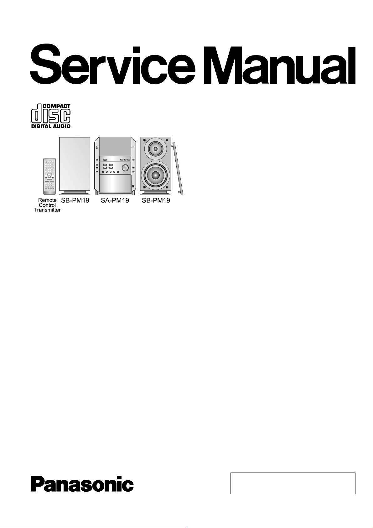
CD Stereo System
SA-PM19E
SA-PM19EB
SA-PM19EG
Colour
(S)... Silver Type
(K)... Black Type (For E only)
ORDER NO. MD0403117C2
Specification
n Amplifier Section
RMS Power output
10% Total harmonic distortion
1 kHz, both channels driven
(Low channel) 35 W per channel (6 Ω)
8 kHz, both channels driven
(High channel) 35 W per channel (6 Ω)
Total Bi-Amp power 70 W per channel
Output Impedance
Headphone 16Ω -32Ω
n FM Tuner Section
Frequency range 87.50 - 108.00 MHz (50 kHz
steps)
Sensitivity 1.5 µV (IHF)
S/N 26 dB 1.5 µV
ntenna terminal(s) 75 Ω (unbalanced)
n AM Tuner Section
Frequency range 522 kHz - 1629 kHz (9 kHz
steps)
520 kHz - 1630 kHz (10 kHz
steps)
Sensitivity
S/N 20 dB (at 999 kHz) 560 µV/m
n Cassette Deck Section
Track system 4 track, 2 channel
Heads
Record/playback Solid permalloy head
Erasure Double gap ferrite head
Motor DC servo motor
Recording system AC bias 100 kHz
Erasing system AC erase 100 kHz
Tape speed 4.8 cm/s
Overall frequency response (+3 dB, -6 dB at Deck Out)
Normal (Type I) 35 Hz - 14 kHz
S/N RATIO 45 dB (A weighted)
Wow and flutter 0.10% (WRMS)
Fast forward and rewind times Approx. 120 seconds with C-60
cassette tape
n CD Section
Disc
CD, CD-R, CD-RW, MP3 8cm/12cm
Sampling frequency 44.1 kHz
Decoding 16 bit linear
Pickup
Beam source/ Wavelength Semiconductor laser / 780 nm
Number of channels Stereo
Frequency response 20 Hz - 20 kHz (+1dB, -2dB)
Wow and flutter Below measurable limit
Digital filter 8fs
© 2004 Panasonic AVC Networks Singapore Pte.
Ltd. All rights reserved. Unauthorized copying and
distribution is a violation of law.
Page 2
SA-PM19E / SA-PM19EB / SA-PM19EG
D/A converter MASH (1 bit DAC)
MP3
Bit rate 32kbps-320kbps
Sampling frequency 32kHz, 44.1kHz, 48kHz
n General
Power supply AC 230 V, 50 Hz (E, EG)
AC 230 V - 240 V, 50 Hz (EB)
Power consumption 130 W
Dimensions (W x H x D) 179 x 250 x 383 mm
Mass 5.24 kg
Power consumption in standby mode: 0.8W
n System: SC-PM19E-S
Music Center: SA-PM19E-S
Speaker: SB-PM19E-M
n System: SC-PM19EB-S
n System: SC-PM19EG-S
n System: SC-PM19E-K
Notes:
1. Specifications are subject to change without notice.
Mass and dimensions are approximate.
2. Total harmonic distortion is measured by the digital spectrum
analyzer.
3. The labels “HIGH” and “LOW” on the rear of the speakers refer
to High frequency and Low frequency.
Music Center: SA-PM19EB-S
Speaker: SB-PM19E-M
Music Center: SA-PM19EG-S
Speaker: SB-PM19EG-M
Music Center: SA-PM19E-S
Speaker: SB-PM19P-K
CONTENTS
Page Page
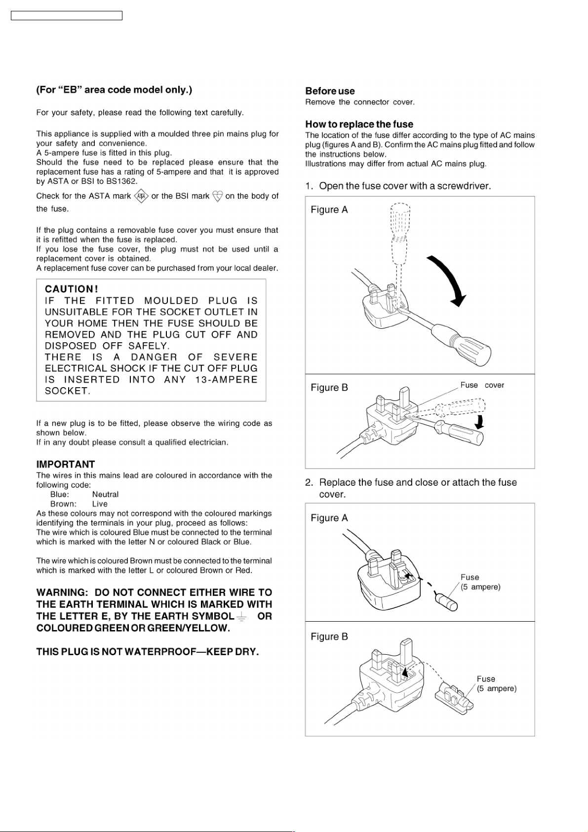
1 Caution for AC Mains Lead
2 Before Repair and Adjustment
3 Protection Circuitry
4 Handling the Lead-free Solder
4.1. About lead free solder (PbF)
5 Precaution of Laser Diode
6 Handling Precautions For Traverse Deck
7 Accessories
8 Operation Procedures
9 Assembling and Disassembling
9.1. Disassembly flow chart
9.2. Disassembly of Side Panel L & R
9.3. Disassembly of Top Cabinet
9.4. Disassembly of Deck P.C.B. & Tape Eject P.C.B.
9.5. Disassembly of Front Panel
9.6. Disassembly of Panel P.C.B., Headphone P.C.B. and
Switch P.C.B.
9.7. Disassembly of Tact Switch P.C.B.
9.8. Disassembly of Rear Panel
9.9. Disassembly of Main P.C.B.
9.10. Disassembly of Transformer P.C.B.
9.11. Disassembly of Speaker Terminal P.C.B
9.12. Disassembly of Power P.C.B
9.13. Disassembly of CR16 Mechanism
9.14. Checking Procedure for Each Major P.C.B.
9.15. Procedure for Replacing Cassette Holder
9.16. Procedure for Replacing Pinch Roller and Head Block
(Cassette Mechanism Unit)
9.17. Procedure for Replacing Motor, Capstan Belt A, Capstan
Belt B, and Winding Belt (Cassette Mechanism Unit)
4
5
5
6
6
7
8
9
10
11
11
12
12
12
13
13
14
14
14
15
15
15
15
17
17
18
19
9.18. Procedure for Replacing Parts on Mechanism PCB
9.19. Replacement of CD traverse deck
9.20. Replacement of optical pickup unit (CD mechanism)
9.21. Replacement of a traverse gear A and a traverse gear B
9.22. Procedure for removing CD loading mechanism
9.23. CR16 mechanism disassembly procedure
9.24. CR16 MECHANISM ASSEMBLY PROCEDURE
9.25. Disassembly of traverse mechanism
9.26. Handling of cassette tape jam
10 Service Positions
10.1. Checking procedure
10.2. Checking the major P.C.B.
11 Self-Diagn ostic Display Function
11.1. Preparations
11.2. Setting of the Self-Diagnostic Mode
11.3. Restoring Normal Display
11.4. Clearing Self-Diagnostic Memory
11.5. Displaying Self-Diagnostic Results
12 Procedure for Checking Operation of Individual Parts of
Cassette Mechanism Unit
12.1. Operation Check with Cassette Tape
12.2. Operation Check without Cassette Tape
13 Measurem ent And Adjustments
13.1. Tuner/CD Sections
13.2. Cassette Deck Section
14 Block Diagram
14.1. CD Servo Block
14.2. Main Block
15 Notes of Schematic Diagram
20
21
22
23
24
24
31
43
44
45
45
45
46
46
46
46
46
46
49
49
49
51
51
51
53
53
55
60
2
Page 3
SA-PM19E / SA-PM19EB / SA-PM19EG
16 Schematic Diagram 61
16.1. CD Servo Circuit
16.2. Main Circuit
61
63
16.3. Panel Circuit, Tact Switch Circuit, Switch Circuit and
Headphone Circuit
67
16.4. Cassette Deck Circuit, Deck Mechanism Circuit and Tape
Eject Circuit
16.5. Power Circuit
16.6. Transformer Circuit and Speaker Terminal Circuit
16.7. CD Loading Circuit
17 Printed Circuit Board
17.1. CD Servo P.C.B. (SIDE A and SIDE B)
17.2. Main P.C.B.
17.3. Panel P.C.B. and Tact Switch P.C.B.
69
71
74
75
76
76
78
80
17.4. Switch P.C.B., Headphone P.C.B. and Speaker Terminal
P.C.B.
17.5. Deck P.C.B. and Tape Eject P.C.B.
17.6. Deck Mechanism P.C.B. and CD Loading P.C.B.
81
82
83
17.7. Power P.C.B.
17.8. Transformer P.C.B.
18 Wiring Connection Diagram
19 Illustration of IC 痴, Transistors and Diodes
20 Terminal Function of ICエs
20.1. IC701 (AN22004A-NF) IC HEAD AMP
20.2. IC702 (MN6627934CH) IC LSI
20.3. IC703 (BA5948FPE2) IC 4CH DRIVE
20.4. IC302 (C2CBJF000016) MICRO PROCESSOR
21 Troubleshooting Flowchart (CD Section Circuit)
22 Parts Location and Replacement Parts List
22.1. Deck Mechanism
22.2. CD Loading Mechanism
22.3. Cabinet
22.4. Electrical Part List
22.5. Packaging Materials & Accessories Parts List
22.6. Packaging
84
85
86
88
89
89
89
90
90
92
94
95
97
102
105
113
113
3
Page 4
SA-PM19E / SA-PM19EB / SA-PM19EG
1 Caution for AC Mains Lead
4
Page 5

SA-PM19E / SA-PM19EB / SA-PM19EG
2 Before Repair and Adjustment
Disconnect AC power, discharge Power Supply Capacitors C506, C507, C508, C584 & C311 through a 10Ω, 5W resistor to ground.
DO NOT SHORT-CIRCUIT DIRECTLY (with a screwdriver blade, for instance), as this may destroy solid state devices.
After repairs are completed, restore power gradually using a variac, to avoid overcurrent.
· Current consumption at AC 230V, 50 Hz in NO SIGNAL mode should be ~300 mA. (For E, EG)
· Current consumption at AC 230V - 240V, 50 Hz in NO SIGNAL mode should be ~300 mA. (For EB)
3 Protection Circuitry
The protection circuitry may have operated if either of the following conditions are noticed:
· No sound is heard when the power is turned on.
· Sound stops during a performance.
The function of this circuitry is to prevent circuitry damage if, for example, the positive and negative speaker connection wires are
"shorted", or if speaker systems with an impedance less than the indicated rated impedance of the amplifier are used.
If this occurs, follow the procedure outlines below:
1. Turn off the power.
2. Determine the cause of the problem and correct it.
3. Turn on the power once again after one minute.
Note:
When the protection circuitry functions, the unit will not operate unless the power is first turned off and then on again.
5
Page 6

SA-PM19E / SA-PM19EB / SA-PM19EG
4 Handling the Lead-free Solder
4.1. About lead free solder (PbF)
Distinction of PbF P.C.B.:
P.C.B.s (manufactured) using lead free solder will have a PbF stamp on the P.C.B.
Caution:
· Pb free solder has a higher melting point than standard solder; Typically the melting point is 50 - 70°F (30 - 40°C) higher. Please
use a high temperature soldering iron. In case of soldering iron with temperature control, please set it to 700 ± 20°F (370 ±
10°C).
· Pb free solder will tend to splash when heated too high (about 1100°F/600°C).
· When soldering or unsoldering, please completely remove all of the solder on the pins or solder area, and be sure to heat the
soldering points with the Pb free solder until it melts enough.
6
Page 7
SA-PM19E / SA-PM19EB / SA-PM19EG
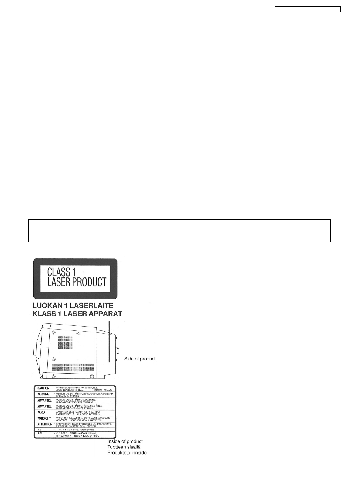
5 Precaution of Laser Diode
Caution :
This product utilizes a laser diode with the unit turned "ON", invisible laser radiation is emitted from the pick up lens.
Wavelength : 780 nm
Maximum output radiation power from pick up : 100 µW/VDE
Laser radiation from pick up unit is safety level, but be sure the followings:
1. Do not disassemble the optical pick up unit, since radiation from exposed laser diode is dangerous.
2. Do not adjust the variable resistor on the pick up unit. It was already adjusted.
3. Do not look at the focus lens using optical instruments.
4. Recommend not to look at pick up lens for a long time.
ACHTUNG :
Dieses Produkt enthält eine Laserdiode. Im eingeschalteten Zustand wird unsichtbare Laserstrahlung von der Lasereinheit
abgestrahlt.
Wellenlänge : 780nm
Maximale Strahlungsleistung der Lasereinheit :100µW/VDE
Die Strahlung an der Lasereinheit ist ungefährlich, wenn folgende Punkte beachtet werden:
1. Die Lasereinheit nicht zerlegen, da die Strahlung an der freigelegten Laserdiode gefährlich ist.
2. Den werkseitig justierten Einstellregler der Lasereinhit nicht verstellen.
3. Nicht mit optischen Instrumenten in die Fokussierlinse blicken.
4. Nicht über längere Zeit in die Fokussierlinse blicken.
ADVARSEL :
I dette a apparat anvendes laser.
CAUTION!
THIS PRODUCT UTILIZES A LASER.
USE OF CONTROLS OR ADJUSTMENTS OR PERFORMANCE OF PROCEDURES OTHER THAN THOSE SPECIFIED HEREIN MAY RESULT
IN HAZARDOUS RADIATION EXPOSURE.
n Use of Caution Labels
7
Page 8
SA-PM19E / SA-PM19EB / SA-PM19EG
6 Handling Precautions For Traverse Deck
The laser diode in the traverse deck (optical pickup) may break
down due to potential difference caused by static electricity of
clothes or human body.
So, be careful of electrostatic breakdown during repair of the
traverse deck (optical pickup).
l Handling of CD traverse deck (optical pickup)
1. Do not subject the traverse deck (optical pickup) to
static electricity as it is extremely sensitive to electrical
shock.
2. The short land between the No.4 (LD) and No.5 (GND)
pins on the flexible board (FFC) is shorted with a solder
build-up to prevent damage to the laser diode (Fig 1).
3. Take care not to apply excessive stress to the flexible
board (FPC board).
4. Do not turn the variable resistor (laser power
adjustment). It has already been adjusted.
Fig 1
l Grounding for electrostatic breakdown prevention
1. Human body grounding (Fig 2)
Use the anti-static wrist strap to discharge the static
electricity from your body.
2. Work table grounding (Fig 2)
Put a conductive material (sheet) or steel sheet on the
area where the traverse deck (optical pickup) is placed,
and ground the sheet.
Caution :
The static electricity of your clothes will not be grounded
through the wrist strap. So, take care not to let your
clothes touch the traverse deck (optical pickup).
Fig 2
Caution when Replacing the Optical Pickup :
The traverse has a short point shorted with solder to protect
the laser diode against electrostatics breakdown. Be sure to
remove the solder from the short point before making
connections.
8
Page 9
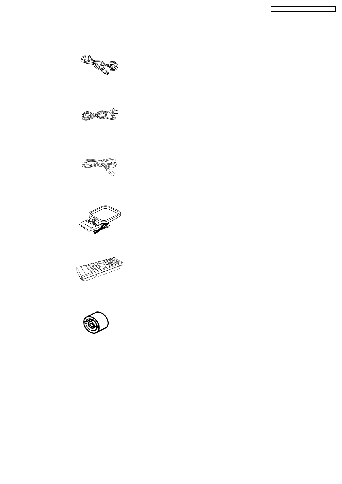
7 Accessories
Note : Refer to Packing Materials & Accessories for part number.
AC mains lead (For
EB only)
ACmains lead
(For E & EG
only)
SA-PM19E / SA-PM19EB / SA-PM19EG
FM indoor
antenna
AM loop antenna
Remote control
transmitter
Antenna plug
adaptor (For EB
only)
9
Page 10
SA-PM19E / SA-PM19EB / SA-PM19EG
8 Operation Procedures
10
Page 11
SA-PM19E / SA-PM19EB / SA-PM19EG
9 Assembling and Disassembling
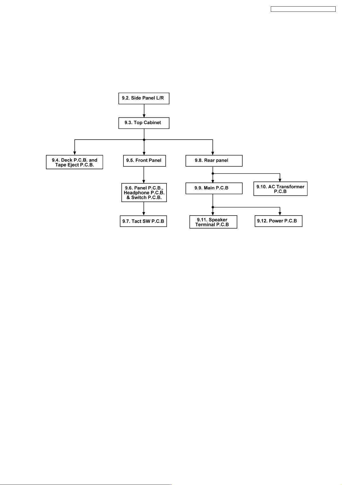
9.1. Disassembly flow chart
The following chart is the procedure for disassembling the casing and inside parts for internal inspection when carrying out the
servicing.
To assemble the unit, reverse the steps shown in the chart below.
11
Page 12
SA-PM19E / SA-PM19EB / SA-PM19EG
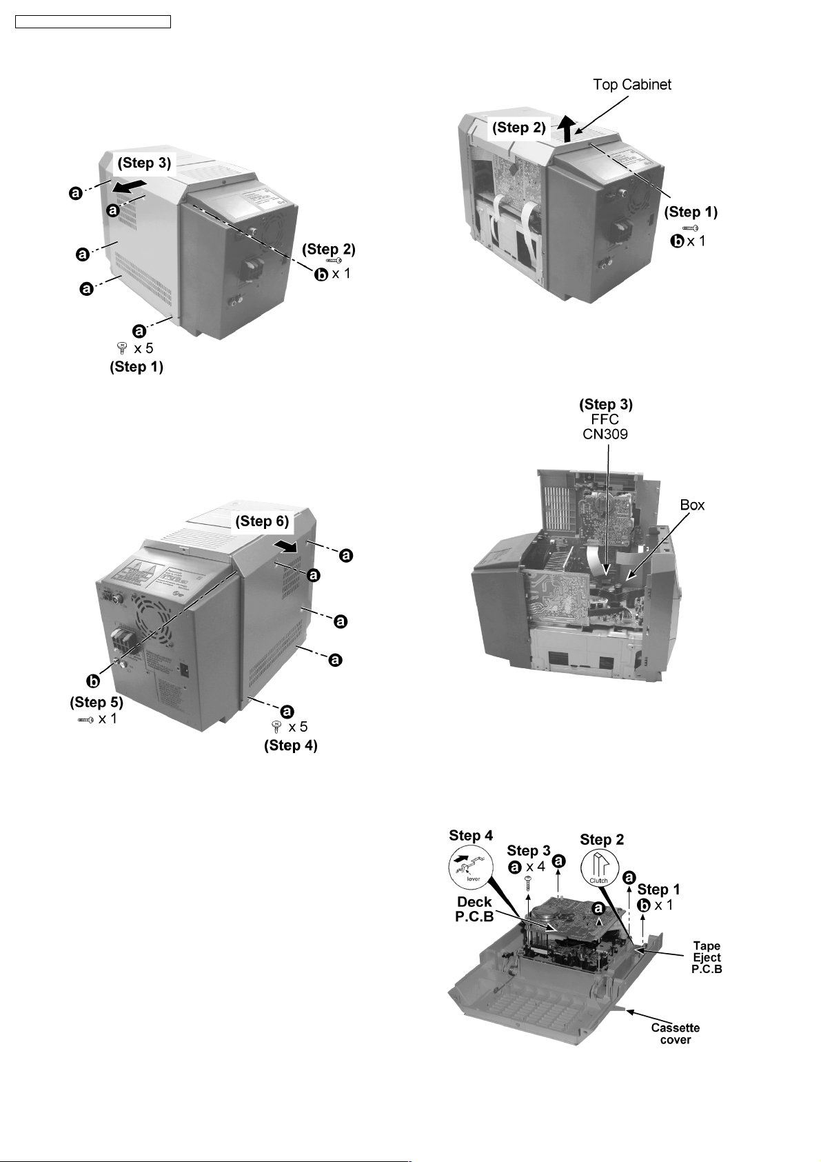
9.2. Disassembly of Side Panel L &
R
Step 1 : Remove all the screws.
Step 2 : Remove the screw.
Step 3 : Remove the panel L as arrow shown.
Step 1 : Remove the screws.
Step 2 : Lift up the Top Cabinet and push backward as arrow
shown, flip Top Cabinet sideway.
Step 4 : Remove all the screws.
Step 5 : Remove the screw.
Step 6 : Remove the panel R as arrow shown.
9.3. Disassembly of Top Cabinet
· Follow the (Step 1) - (Step 6) of Item 9.2.
Step 3 : Detach the FFC Connector Board CN309.
9.4. Disassembly of Deck P.C.B. &
Tape Eject P.C.B.
· Follow the (Step 1) - (Step 6) of Item 9.2.
· Follow the (Step 1) - (Step 3) of Item 9.3.
Step 1 : Remove the screw.
12
Page 13
Step 2 : Release the clutch.
Step 3 : Remove all the screws.
Step 4 : Press the lever as arrow shown and remove the Deck
Mechanism.
9.5. Disassembly of Front Panel
· Follow the (Step 1) - (Step 6) of Item 9.2.
· Follow the (Step 1) - (Step 3) of Item 9.3.
SA-PM19E / SA-PM19EB / SA-PM19EG
Step 1 : Detach the FFC Board (CN308).
Step 2 : Detach the wire at CN505 Connector.
Step 3 : Release all the Claw.
Step 4 : Push the Front Panel as arrow shown.
9.6. Disassembly of Panel P.C.B.,
Headphone P.C.B. and Switch
P.C.B.
· Follow the (Step 1) - (Step 6) of Item 9.2.
· Follow the (Step 1) - (Step 3) of Item 9.3.
· Follow the (Step 1) - (Step 4) of Item 9.5.
Step 1 : Remove all the screws.
13
Page 14
SA-PM19E / SA-PM19EB / SA-PM19EG
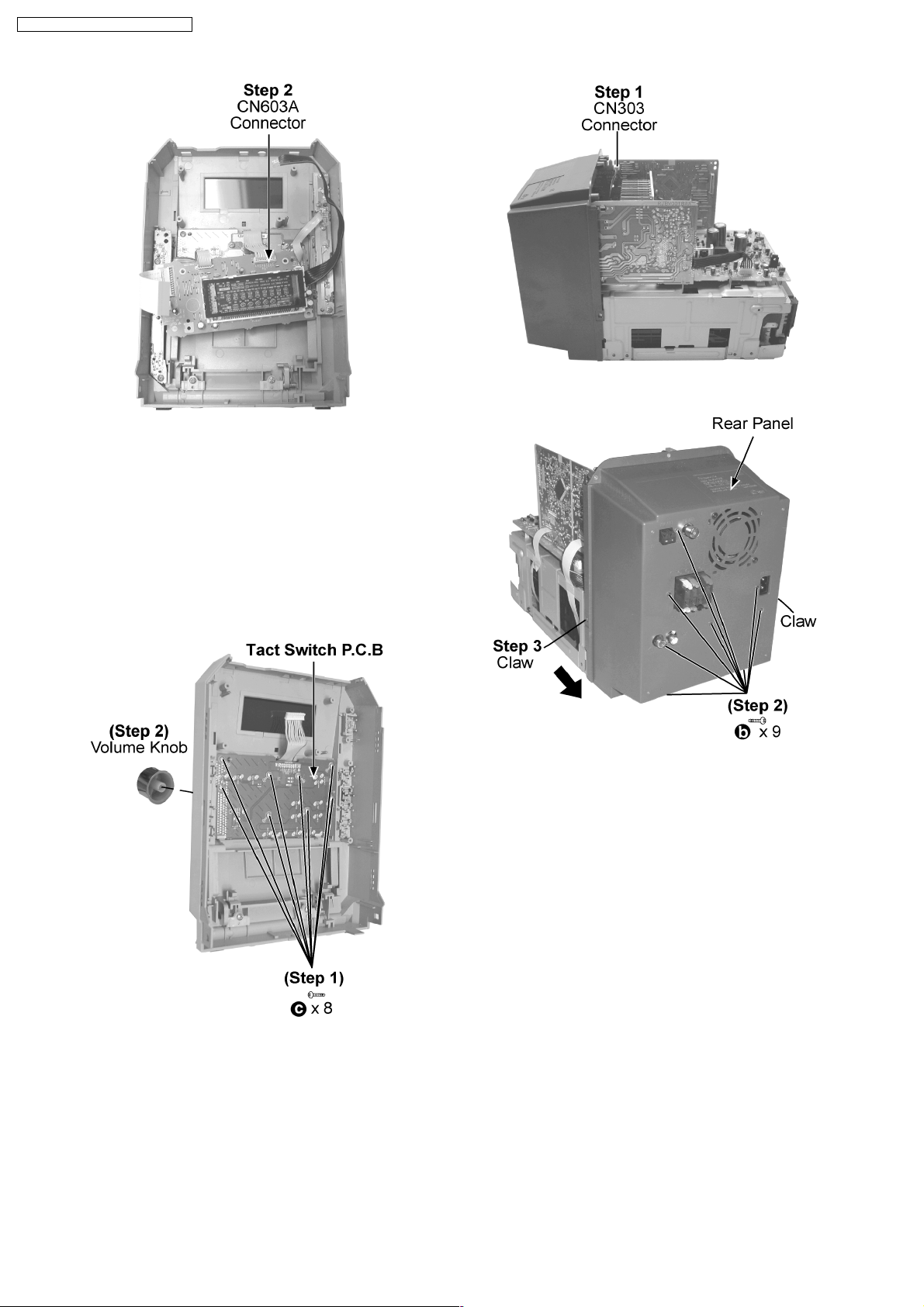
Step 2 : Detach the CN603A Connector.
Step 1 : Detach the wire at CN303 Connector.
9.7. Disassembly of Tact Switch
P.C.B.
· Follow the (Step 1) - (Step 6) of Item 9.2.
· Follow the (Step 1) - (Step 3) of Item 9.3.
· Follow the (Step 1) - (Step 4) of Item 9.5.
· Follow the (Step 1) - (Step 2) of Item 9.6.
Step 2 : Remove all the screws.
Step 3 : Release the Claws and remove Rear Panel as arrows
shown.
9.9. Disassembly of Main P.C.B.
· Follow the (Step 1) - (Step 6) of Item 9.2.
· Follow the (Step 1) - (Step 3) of Item 9.3.
· Follow the (Step 1) - (Step 4) of Item 9.5.
· Follow the (Step 1) - (Step 3) of Item 9.8.
Step 1 : Remove all the screws.
Step 2 : Remove the Volume Knob.
9.8. Disassembly of Rear Panel
· Follow the (Step 1) - (Step 6) of Item 9.2.
· Follow the (Step 1) - (Step 3) of Item 9.3.
· Follow the (Step 1) - (Step 4) of Item 9.5.
14
Page 15
SA-PM19E / SA-PM19EB / SA-PM19EG
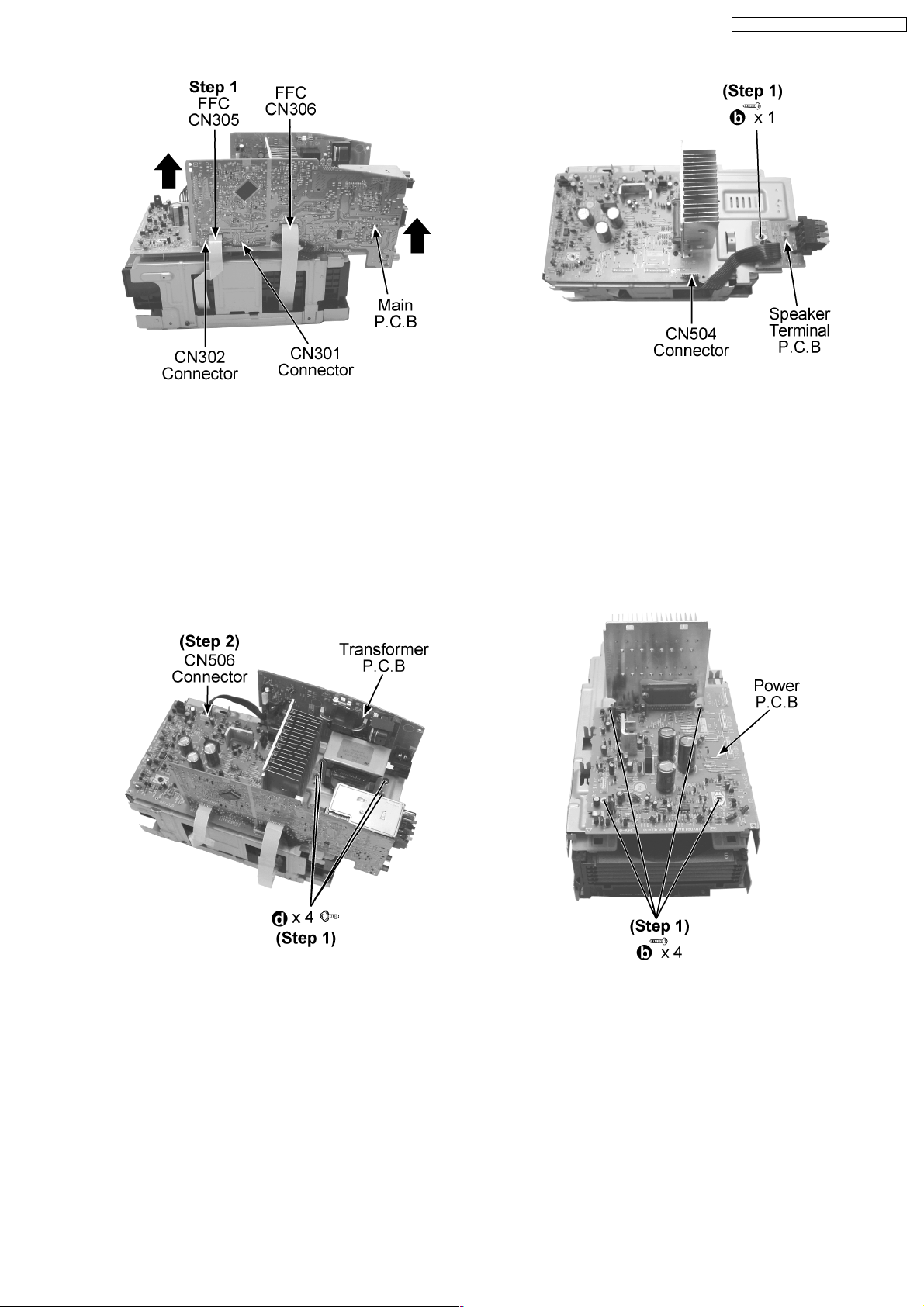
Step 1 : Remove the screw and CN504 Connector.
Step 1 : Remove the CN301, CN302 Connector and FFC
CN305, CN306 .
Step 2 : Remove the Main P.C.B as arrow shown.
9.10. Disassembly of Transformer
P.C.B.
· Follow the (Step 1) - (Step 6) of Item 9.2.
· Follow the (Step 1) - (Step 3) of Item 9.3.
· Follow the (Step 1) - (Step 4) of Item 9.5.
· Follow the (Step 1) - (Step 3) of Item 9.8.
9.12. Disassembly of Power P.C.B
· Follow the (Step 1) - (Step 6) of Item 9.2.
· Follow the (Step 1) - (Step 3) of Item 9.3.
· Follow the (Step 1) - (Step 4) of Item 9.5.
· Follow the (Step 1) - (Step 3) of Item 9.8.
· Follow the (Step 1) - (Step 2) of Item 9.9.
· Follow the (Step 1) - (Step 2) of Item 9.10.
· Follow the (Step 1) of Item 9.11.
Step 1 : Remove all the screws.
Step 2 : Detach the CN506 Connector.
9.11. Disassembly of Speaker
Terminal P.C.B
· Follow the (Step 1) - (Step 6) of Item 9.2.
· Follow the (Step 1) - (Step 3) of Item 9.3.
· Follow the (Step 1) - (Step 4) of Item 9.5.
· Follow the (Step 1) - (Step 3) of Item 9.8.
· Follow the (Step 1) - (Step 2) of Item 9.9.
· Follow the (Step 1) - (Step 2) of Item 9.10.
Step 1 : Remove all the screws.
9.13. Disassembly of CR16
Mechanism
· Follow the (Step 1) - (Step 6) of Item 9.2.
· Follow the (Step 1) - (Step 3) of Item 9.3.
· Follow the (Step 1) - (Step 4) of Item 9.5.
· Follow the (Step 1) - (Step 3) of Item 9.8.
· Follow the (Step 1) - (Step 2) of Item 9.9.
· Follow the (Step 1) - (Step 2) of Item 9.10.
15
Page 16
SA-PM19E / SA-PM19EB / SA-PM19EG
· Follow the (Step 1) of Item 9.11.
· Follow the (Step 1) of Item 9.12.
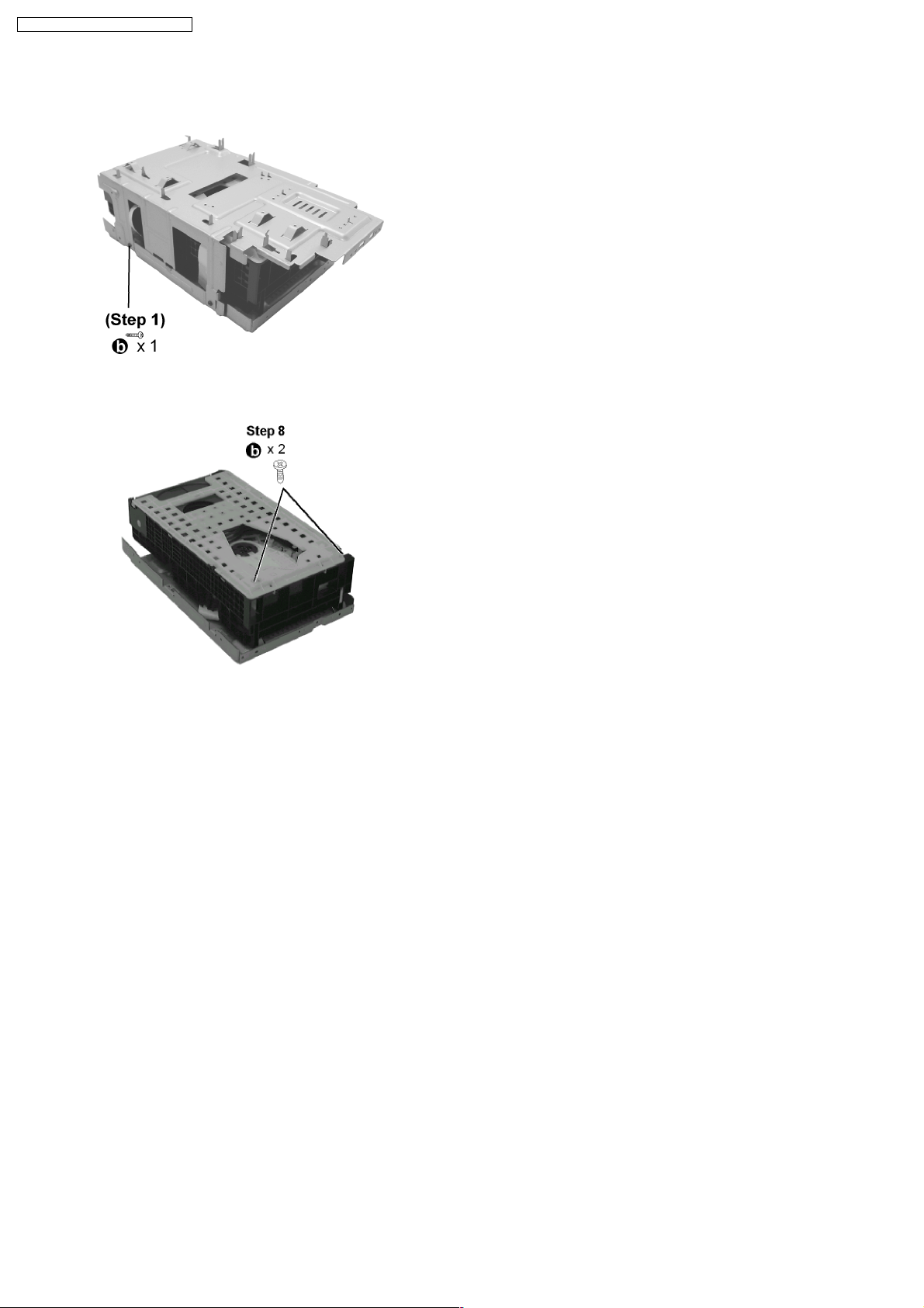
Step 1 : Remove the screw.
Step 2 : Remove 2 screws. Lift up the CD Mecha Unit.
16
Page 17
9.14. Checking Procedure for Each Major P.C.B.
9.14.1. Replacement of the Power Amplifier IC
· Replacement of the Power Amplifier IC
· Follow the (Step 1) - (Step 6) of Item 9.2.
· Follow the (Step 1) - (Step 3) of Item 9.3.
· Follow the (Step 1) - (Step 4) of Item 9.5.
· Follow the (Step 1) - (Step 3) of Item 9.8.
· Follow the (Step 1) - (Step 2) of Item 9.9.
· Follow the (Step 1) - (Step 2) of Item 9.10.
· Follow the (Step 1) of Item 9.11.
· Follow the (Step 1) of Item 9.12.
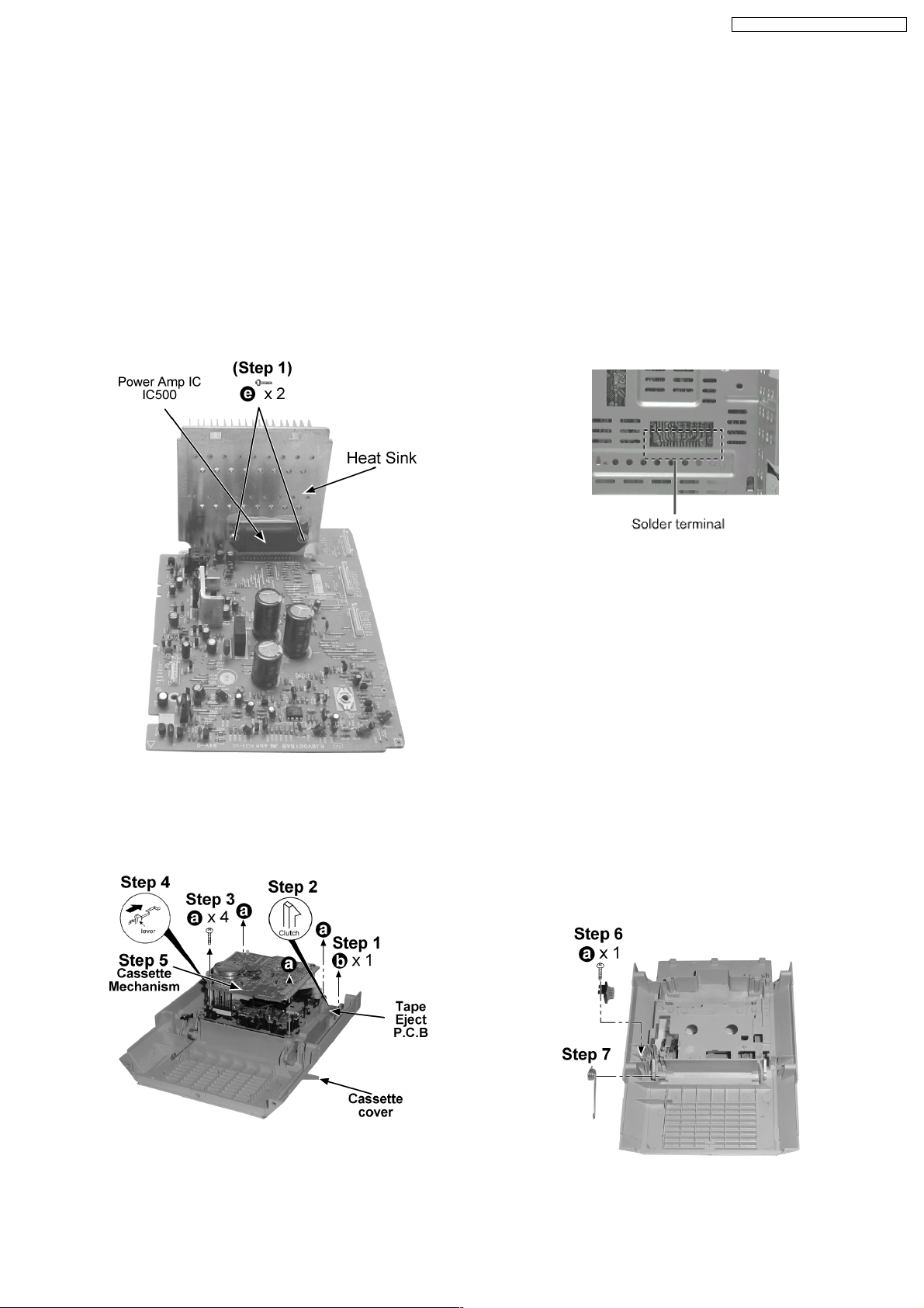
Step 1 : Remove 2 screws fixed to the Power Amp I.C.
SA-PM19E / SA-PM19EB / SA-PM19EG
Step 2 : Unsolder the terminals of Power Amp IC, transistor and
replace the component.
9.15. Procedure for Replacing Cassette Holder
· Follow the (Step 1) - (Step 6) of Item 9.2.
· Follow the (Step 1) - (Step 3) of Item 9.3.
Step 4 : Press the lever to open the cassette cover.
Step 5 : Remove the cassette mechanism unit.
Step 1 : Remove the screw.
Step 2 : Release the clutch.
Step 3 : Remove all the screws.
Step 6 : Remove the screw and damper gear.
17
Page 18
SA-PM19E / SA-PM19EB / SA-PM19EG
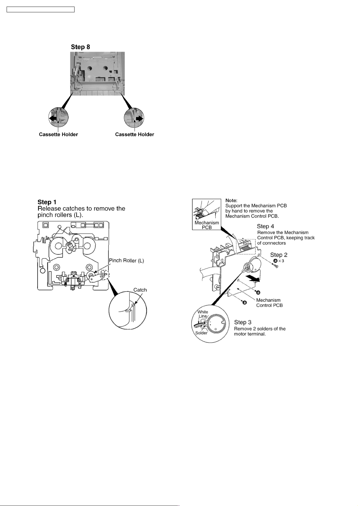
Step 7 : Remove the cassette open spring. Step 8 : Pull out the cassette holder to the direction of the
arrow shown.
9.16. Procedure for Replacing Pinch Roller and Head Block (Cassette
Mechanism Unit)
· Follow the (Step 1) - (Step 6) of Item 9.2.
· Follow the (Step 1) - (Step 3) of Item 9.3.
· Follow the (Step 1) - (Step 5) of Item 9.15.
18
Page 19
SA-PM19E / SA-PM19EB / SA-PM19EG
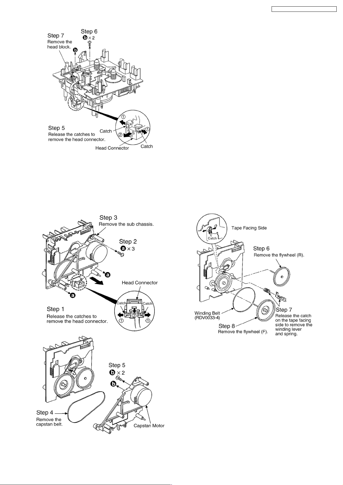
9.17. Procedure for Replacing Motor, Capstan Belt A, Capstan Belt B, and
Winding Belt (Cassette Mechanism Unit)
· Follow the (Step 1) - (Step 6) of Item 9.2.
· Follow the (Step 1) - (Step 3) of Item 9.3.
· Follow the (Step 1) - (Step 5) of Item 9.15.
· Follow the (Step 1) - (Step 5) of Item 9.16.
19
Page 20
SA-PM19E / SA-PM19EB / SA-PM19EG
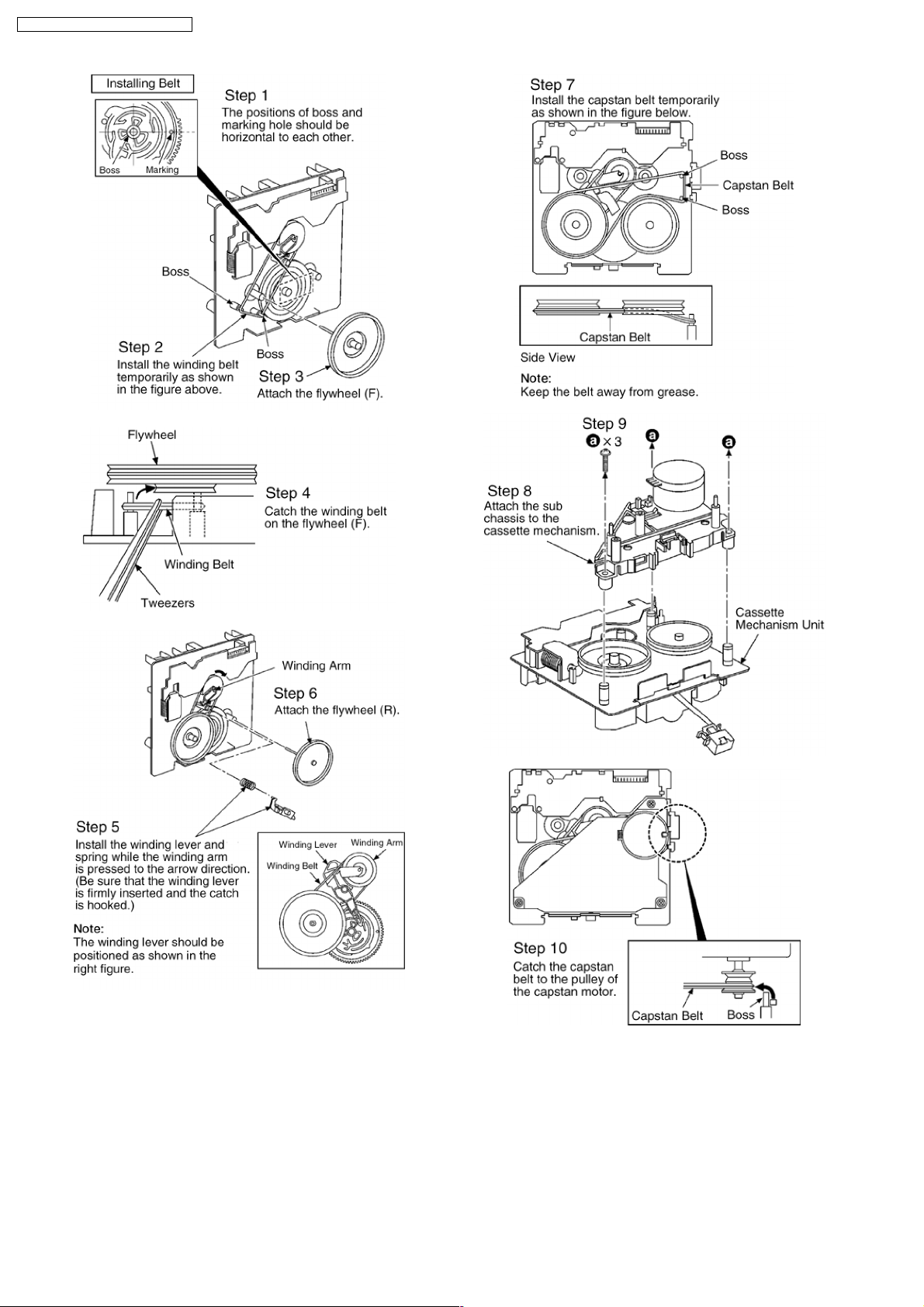
9.18. Procedure for Replacing Parts on Mechanism PCB
· Follow the (Step 1) - (Step 6) of Item 9.2.
· Follow the (Step 1) - (Step 3) of Item 9.3.
· Follow the (Step 1) - (Step 5) of Item 9.15.
· Follow the (Step 1) - (Step 5) of Item 9.16.
20
Page 21
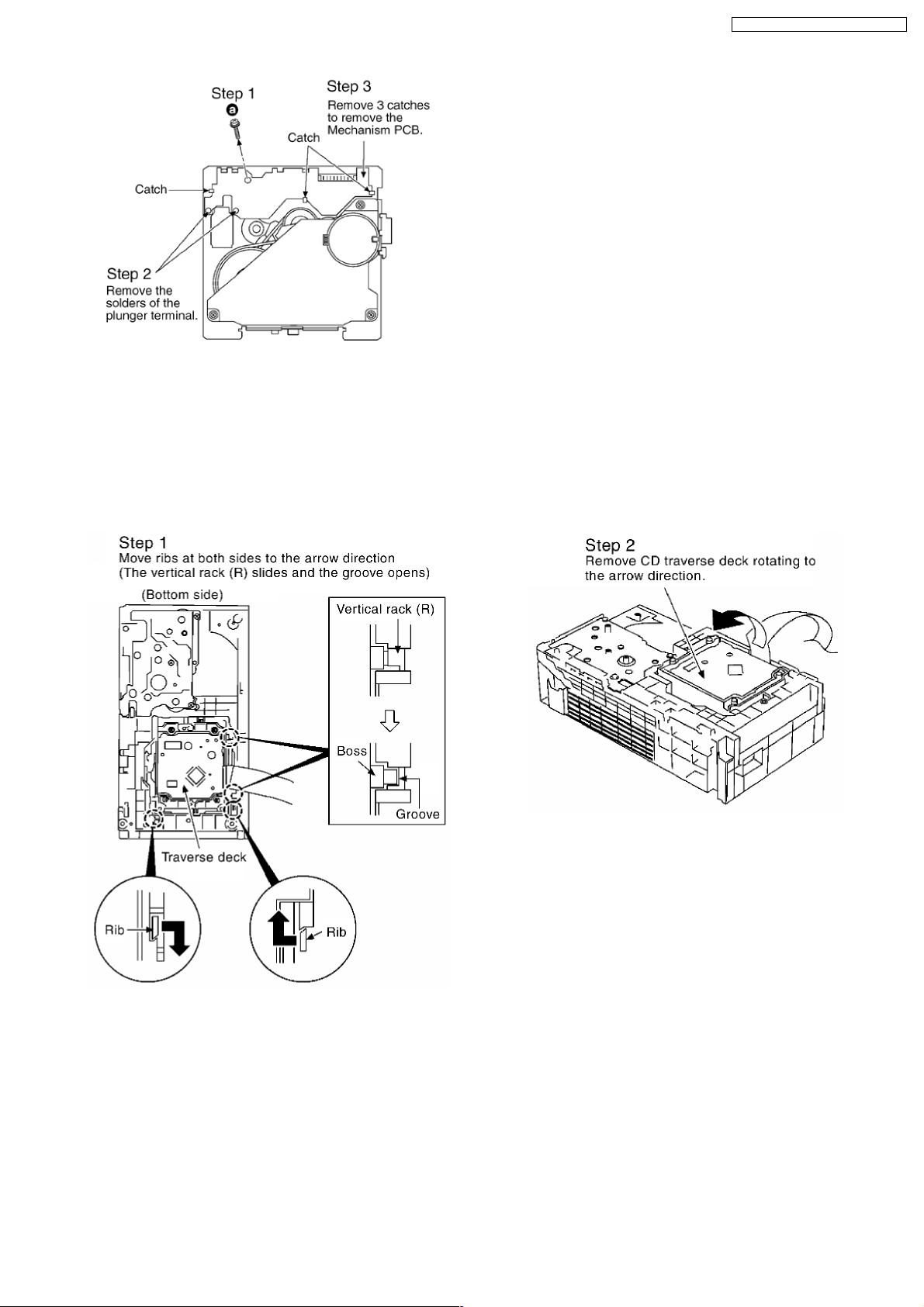
9.19. Replacement of CD traverse deck
· Follow the (Step 1) - (Step 6) of Item 9.2.
· Follow the (Step 1) - (Step 3) of Item 9.3.
· Follow the (Step 1) - (Step 4) of Item 9.5.
· Follow the (Step 1) - (Step 3) of Item 9.8.
· Follow the (Step 1) of Item 9.9.
· Follow the (Step 1) - (Step 2) of Item 9.13.
SA-PM19E / SA-PM19EB / SA-PM19EG
21
Page 22
SA-PM19E / SA-PM19EB / SA-PM19EG
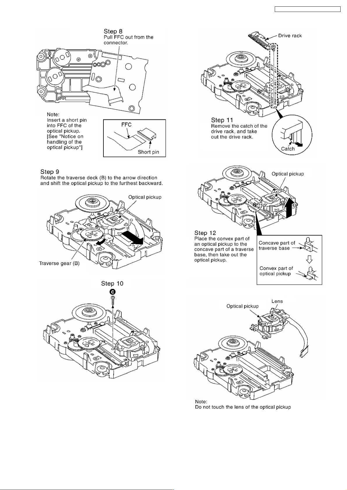
9.20. Replacement of optical pickup unit (CD mechanism)
· Follow the (Step 1) - (Step 6) of Item 9.2.
· Follow the (Step 1) - (Step 3) of Item 9.3.
· Follow the (Step 1) - (Step 4) of Item 9.5.
· Follow the (Step 1) - (Step 3) of Item 9.8.
· Follow the (Step 1) of Item 9.9.
· Follow the (Step 1) - (Step 2) of Item 9.13.
· Follow the (Step 1) - (Step 2) of Item 9.19.
22
Page 23
SA-PM19E / SA-PM19EB / SA-PM19EG
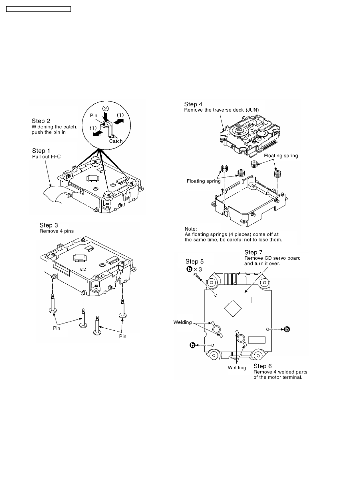
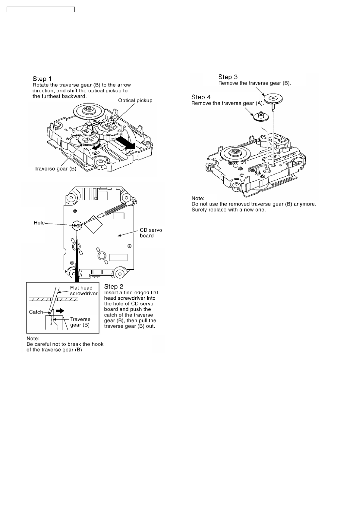
9.21. Replacement of a traverse gear A and a traverse gear B
· Follow the (Step 1) - (Step 6) of Item 9.2.
· Follow the (Step 1) - (Step 3) of Item 9.3.
· Follow the (Step 1) - (Step 4) of Item 9.5.
23
Page 24
SA-PM19E / SA-PM19EB / SA-PM19EG
· Follow the (Step 1) - (Step 3) of Item 9.8.
· Follow the (Step 1) of Item 9.9.
· Follow the (Step 1) - (Step 2) of Item 9.13.
· Follow the (Step 1) - (Step 2) of Item 9.19.
· Follow the (Step 1) - (Step 12) of Item 9.20.
9.22. Procedure for removing CD loading mechanism
1. Turn off by pressing power SW in the body.
2. Unplug AC power cord after the indication of [GOOD-BYE],
then disassemble the body.
3. Disassemble the body, and take out CD loading
mechanism.
4. Perform disassembly according to the following procedure
for disassembly.
9.23. CR16 mechanism disassembly procedure
9.23.1. Gear for servicing information
· This unit has a gear which used for checking items
(open/close of disc tray, up/down operation of traverse unit
by manually) when servicing. (For gear information, that is
described on the items for disassembly procedures.)
· For preparation of gear (for servicing), perform the
procedures as follows.
· In case of re-servicing the same set, the “ gear for servicing”
may be took off because it had been used. So, the “gear for
servicing” must be stored.
1. Remove the gear attached to top cover of CD loading
mechanism.
24
Page 25
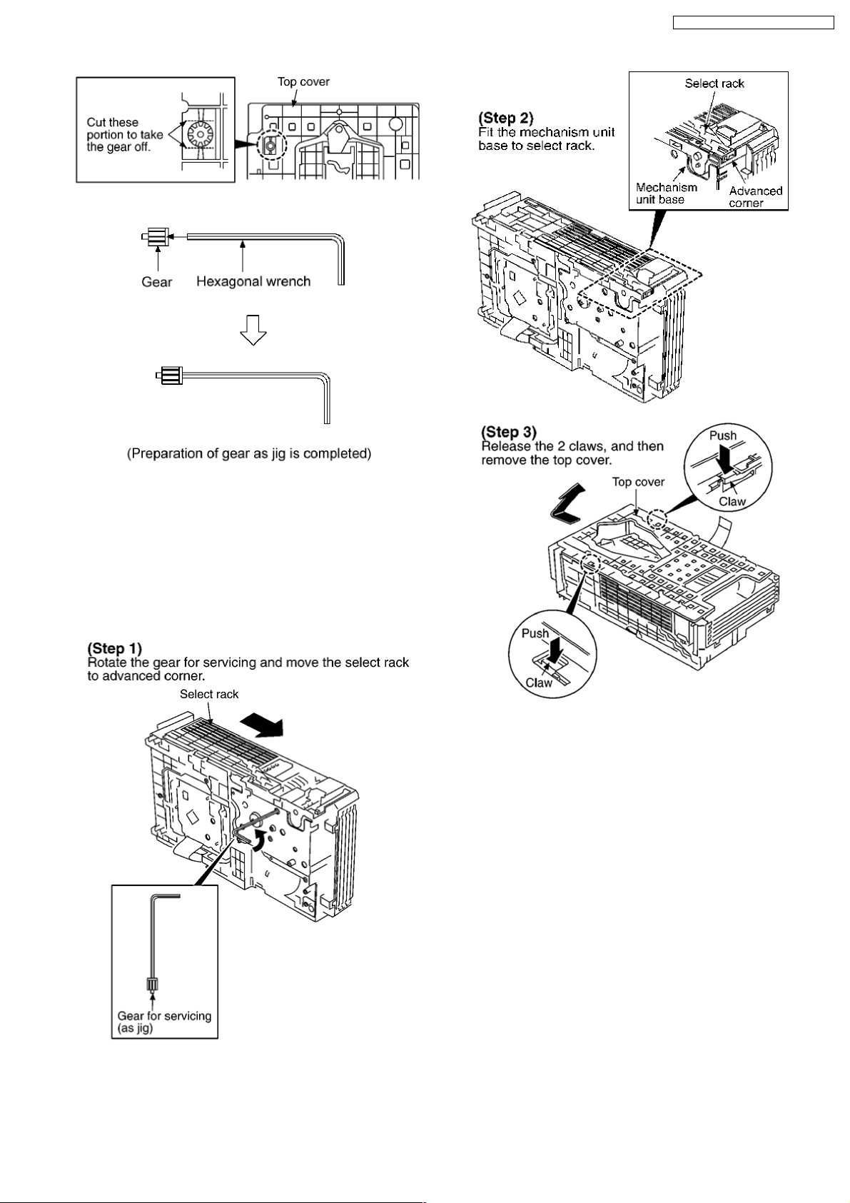
2. Insert the hexgonal wrench (2.5mm) into the gear.
SA-PM19E / SA-PM19EB / SA-PM19EG
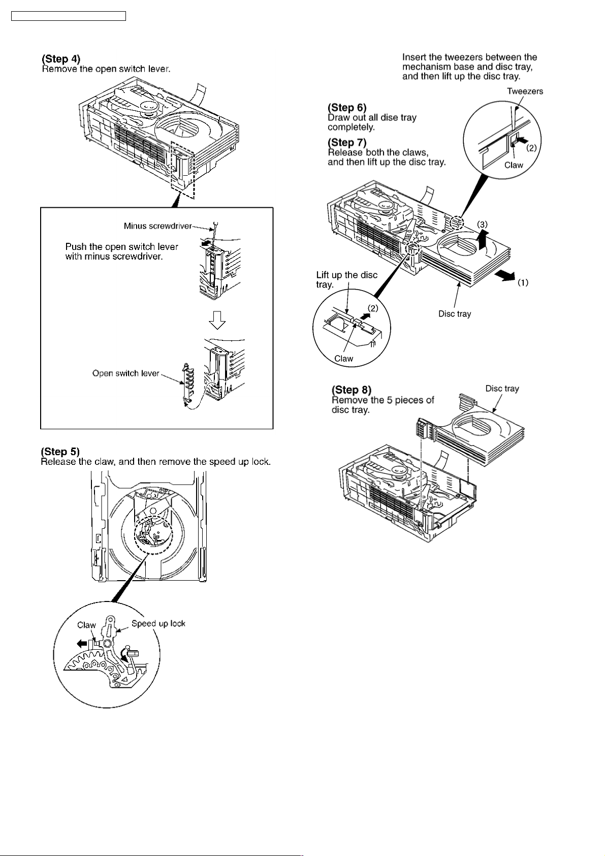
9.23.2. Replacement for the disc tray
· Follow the (Step 1) - (Step 6) of Item 9.2.
· Follow the (Step 1) - (Step 3) of Item 9.3.
· Follow the (Step 1) - (Step 4) of Item 9.5.
· Follow the (Step 1) - (Step 3) of Item 9.8.
· Follow the (Step 1) of Item 9.9.
· Follow the (Step 1) - (Step 2) of Item 9.13.
25
Page 26
SA-PM19E / SA-PM19EB / SA-PM19EG
26
Page 27
SA-PM19E / SA-PM19EB / SA-PM19EG
9.23.3. Replacement for the traverse deck
· Follow the (Step 1) - (Step 6) of Item 9.2.
· Follow the (Step 1) - (Step 3) of Item 9.3.
· Follow the (Step 1) - (Step 4) of Item 9.5.
· Follow the (Step 1) - (Step 3) of Item 9.8.
· Follow the (Step 1) of Item 9.9.
· Follow the (Step 1) - (Step 2) of Item 9.13.
· Follow the (Step 1) - (Step 10) of item 9.23.2.
27
Page 28
SA-PM19E / SA-PM19EB / SA-PM19EG
9.23.4. Disassembly for CD loading unit
· Follow the (Step 1) - (Step 6) of Item 9.2.
· Follow the (Step 1) - (Step 3) of Item 9.3.
· Follow the (Step 1) - (Step 4) of Item 9.5.
· Follow the (Step 1) - (Step 3) of Item 9.8.
· Follow the (Step 1) of Item 9.9.
· Follow the (Step 1) - (Step 2) of Item 9.13.
· Follow the (Step 1) - (Step 10) of item 9.23.2.
· Follow the (Step 1) - (Step 4) of item 9.23.3.
28
Page 29
SA-PM19E / SA-PM19EB / SA-PM19EG
29
Page 30
SA-PM19E / SA-PM19EB / SA-PM19EG
30
Page 31

9.24. CR16 MECHANISM ASSEMBLY
PROCEDURE
The following specified greases and/or oil must be applied
when some specific parts are changed.
1. Floil grease (VFK1298) : The floil grease must be
applied to tray, tray (L) and tray (R).
2. Hanarl oil (VFK1700) : The hanarl oil must be applied to
any parts with grease other than the said parts.
· Follow the (Step 1) - (Step 6) of Item 9.2.
· Follow the (Step 1) - (Step 3) of item 9.3.
· Follow the (Step 1) - (Step 4) of item 9.5.
· Follow the (Step 1) - (Step 3) of item 9.8.
· Follow the (Step 1) of Item 9.9.
· Follow the (Step 1) - (Step 2) of Item 9.13.
· Follow the (Step 1) - (Step 10) of item 9.23.2.
· Follow the (Step 1) - (Step 4) of item 9.23.3.
· Follow the (Step 1) - (Step 22) of item 9.23.4.
SA-PM19E / SA-PM19EB / SA-PM19EG
31
Page 32

SA-PM19E / SA-PM19EB / SA-PM19EG
32
Page 33

SA-PM19E / SA-PM19EB / SA-PM19EG
33
Page 34

SA-PM19E / SA-PM19EB / SA-PM19EG
34
Page 35

SA-PM19E / SA-PM19EB / SA-PM19EG
35
Page 36

SA-PM19E / SA-PM19EB / SA-PM19EG
36
Page 37

SA-PM19E / SA-PM19EB / SA-PM19EG
37
Page 38

SA-PM19E / SA-PM19EB / SA-PM19EG
38
Page 39

SA-PM19E / SA-PM19EB / SA-PM19EG
39
Page 40

SA-PM19E / SA-PM19EB / SA-PM19EG
40
Page 41

SA-PM19E / SA-PM19EB / SA-PM19EG
41
Page 42

SA-PM19E / SA-PM19EB / SA-PM19EG
42
Page 43

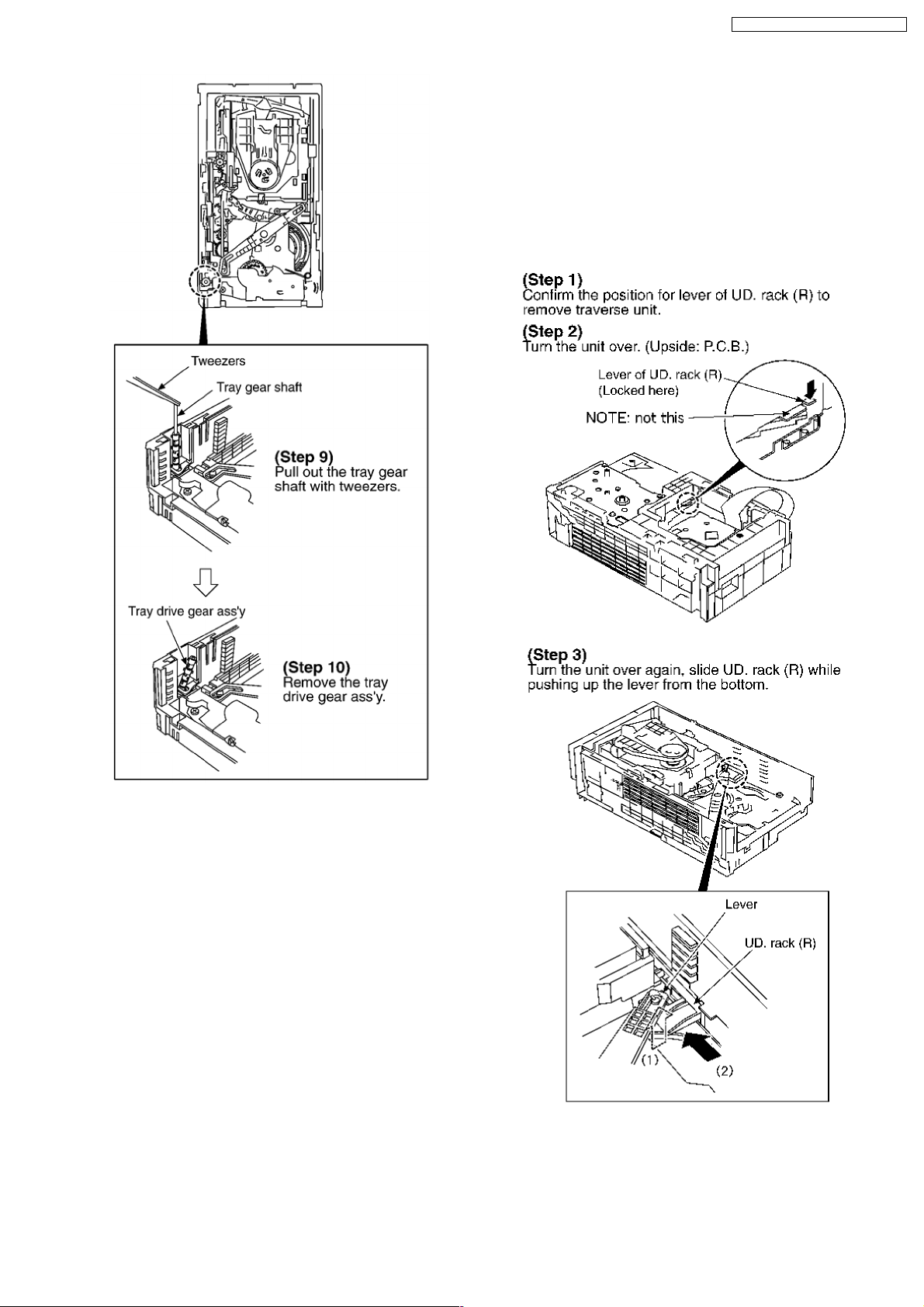
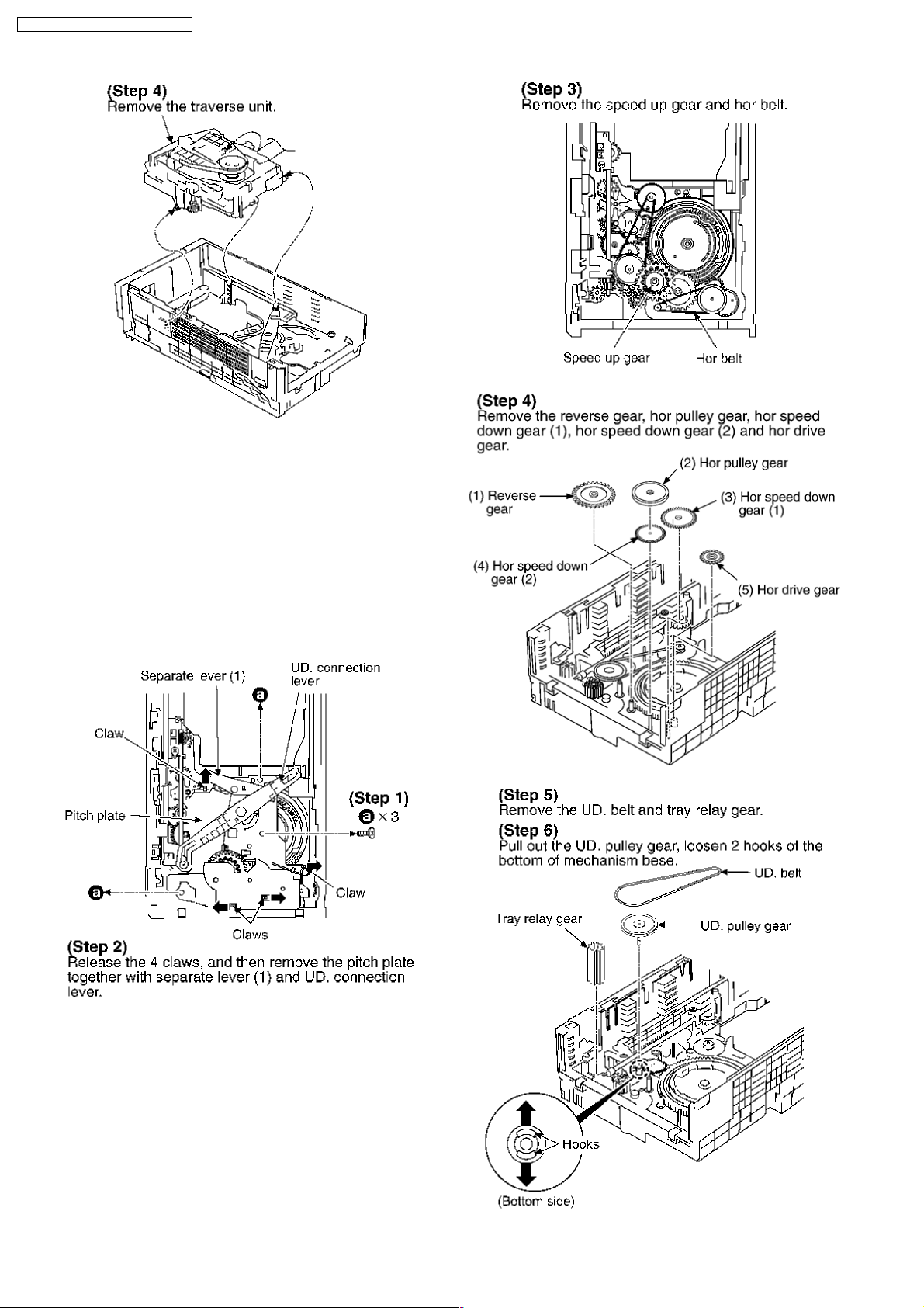
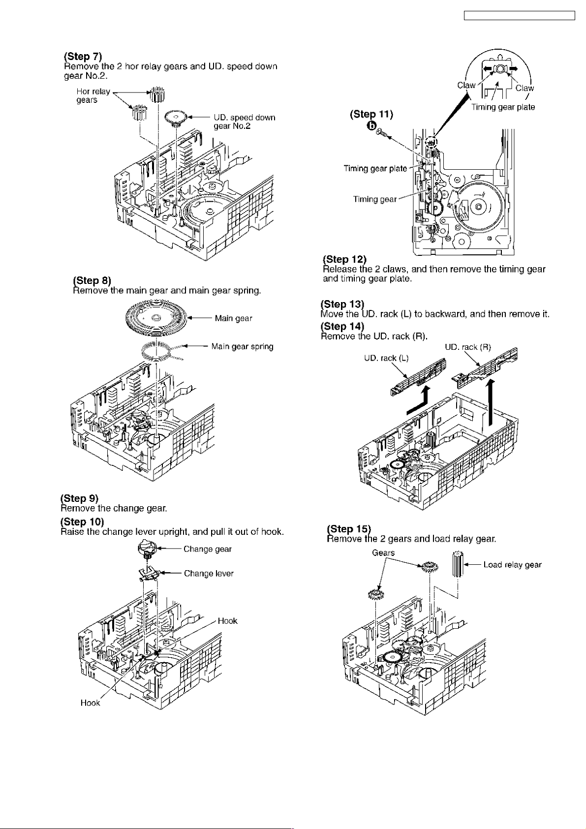
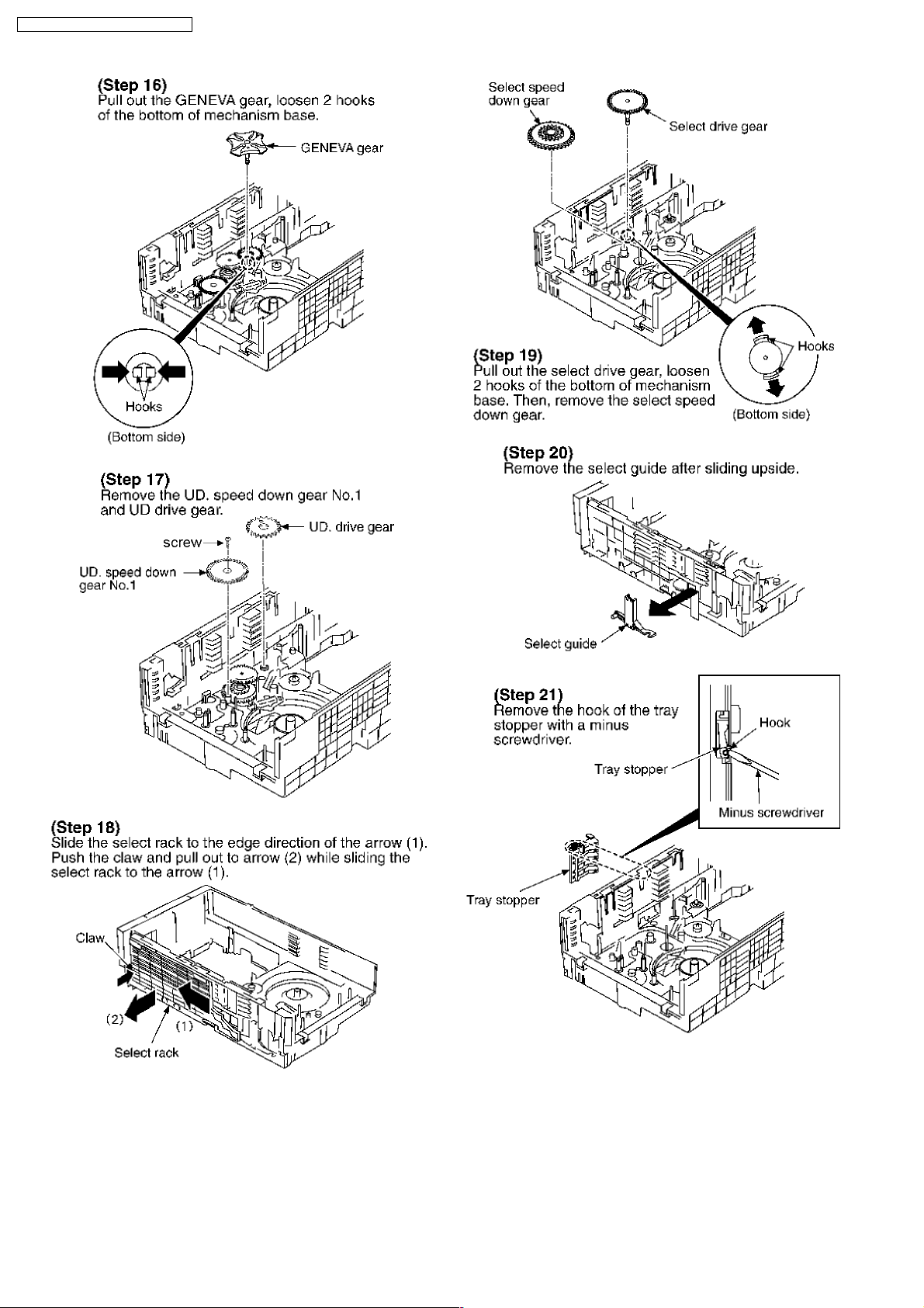
9.25. Disassembly of traverse mechanism
· Follow the (Step 1) - (Step 6) of Item 9.2.
· Follow the (Step 1) - (Step 3) of Item 9.3.
· Follow the (Step 1) - (Step 4) of Item 9.5.
· Follow the (Step 1) - (Step 3) of Item 9.8.
· Follow the (Step 1) of Item 9.9.
· Follow the (Step 1) - (Step 2) of Item 9.13.
· Follow the (Step 1) - (Step 2) of Item 9.19.
SA-PM19E / SA-PM19EB / SA-PM19EG
43
Page 44

SA-PM19E / SA-PM19EB / SA-PM19EG
Step 1 : If the cassette tape is not ejected due to twinng around
capstan or pinch roller during playing or recording, rotate a
flywheel F to the arrow direction to remove twined tape.
Step 2 : Push the lever to the arrow direction, open the
cassette cover and take out the cassette tape.
9.26. Handling of cassette tape jam
· Follow the (Step 1) - (Step 6) of Item 9.2.
44
Page 45

10 Service Positions
10.1. Checking procedure
Note : For the disassembling procedure, see the section 9.
10.2. Checking the major P.C.B.
1. Disassembly of Side Panel L & R
2. Disassembly of Top Cabinet
3. Disassembly of Deck Mechanism
4. Disassembly of Front Panel
5. Disassembly of Panel P.C.B., Headphone P.C.B. and Switch P.C.B.
6. Disassembly of Tact Switch P.C.B.
7. Disassembly of Rear Panel P.C.B.
8. Disassembly of Main P.C.B.
9. Disassembly of Transformer P.C.B.
10. Disassembly of Speaker Terminal P.C.B.
11. Disassembly of Power P.C.B.
12. Disassembly of CR16 Mechanism
SA-PM19E / SA-PM19EB / SA-PM19EG
45
Page 46

SA-PM19E / SA-PM19EB / SA-PM19EG
11 Self-Diagnostic Display Function
This unit is equipped with a self-diagnostic display function, which will be useful during servicing and maintenance.
· Refer to the next page for display symbols, symptoms, etc.
11.1. Preparations
1. A Cr02-positioned blank cassette tape with an erase prevention niche on either Side A or B.
2. A normal-positioned music tape with erase prevention niches on both Sides A and B. Both tapes are halfway forwarded in
advance.
3. The remote controller that comes with this unit.
11.2. Setting of the Self-Diagnostic Mode
No. Operation Procedure Operation and Processing of Microcomputer
1 Switch the SELECTOR to TAPE . There should be NO
cassettes loaded.
2 Press the [STOPn /-DEMO] key for 2 sec and press
/FF/ ] for another 2 sec, it shall enter into the self-
[
diagnostic mode.
11.3. Restoring Normal Display
[T ] shall be displayed in the FL.
· From the F76 display, the normal display does not appear till an error is recovered.
· For displays other than F76, press “POWER” button to turn off the power, and then turn on the power.
11.4. Clearing Self-Diagnostic Memory
<CD Section> (F15, F17, F22, F26, F27, F28, F29)
1. Enter a self-diagnostic mode.
2. Press "STOPn/-DEMO" button. A symbol of self-diagnostic is indicated on the display if an error is found. If several errors are
found, a respective indication is displayed when "STOPn/-DEMO" button is pressing repeatedly. (e.g. H01 → CD F15 → F01)
If no error is found, only "T " indication is displayed and remains unchange even if "STOPn/-DEMO" button is pressed.
11.5. Displaying Self-Diagnostic Results
<Cassette Deck Section> (H01, H02, H03, F01, F02)
1. Enter the self-diagnostic mode, following the instructions described in [11.2. Entering Self-Diagnostic Mode].
2. Insert a normal-positioned music tape with erase prevention niches on both Sides A and B. Press [TAPE
the TPS operation so that the tape automatically stops at an interval between music selections.
3. Press [STOPn /-DEMO] and [TAPE
4. Then, insert a Cr02-positioned blank cassette tape with an erase prevention niche of Side A or B set to the left side.
5. Press [
6. Remove the cassette tape, and set the other side.
7. Press [
8. Press [STOPn/-DEMO] button on the unit.
If an error is found, a self-diagnostic key appears on the display.
If several errors are found, the display shows these keys when [STOPn/-DEMO] button is pressed repeatedly. (Ex.: H01 - H02
- F01 - H01)
/FF/ ] button. The tape will be forwarded and automatically stop after two seconds.
/REW/ ] button. The tape will be rewound and automatically stops after two seconds.
] buttons together on the remote controller. (Recording does not start.)
46
] button to activate
Page 47

SA-PM19E / SA-PM19EB / SA-PM19EG
If no error is found, only the message, “CD TEST” appears on the display.
(*1) TPS operation (music search) detects the blank sections between music selections. Therefore, do not use tapes with the
following conditions:
· A blank section that lasts only 4 seconds or less.
· No blank sections (recording through microphones, etc.).
· Music selections that have extremely low pitches or prolonged silent sections (such as classical music).
· and/or Music recorded with fade in/out effect.
11.5.1. Error detection for CD Block
Error Code Abnormal Items Possible Cause
F15 CD REST SW abnormal CD traverse position intial setting operation failsafe counter (1000 ms) waiting for REST SW to
H15 The CD tray closes CD disc tray detect switch NG. (Check and replace)
F26 CD servo LSI command
signal abnormal
F28 DISC LOAD abnormal While going to play position, if failsafe counter is finished and switch o change or switch
F29 DISC unload abnormal While going to play position, if failsafe counter is finished and switch no change or switch
F27 Slide operation abnormal During vertical operation, if failsafe timer is finished and switch no change or switch target
F17 Down SW abnormal During vertical operation going to the bottom position, if failsafe timer is finished and switch
F22 Loading Mode / Mecha
abnormal
Abnormal item Error Display Method of detection
F75 CD power abnormal Under normal operation (self-diagnostic mode inclusive), check if CDRST is H for SELECTOR
turn on. Error No. shall be clear by force or during coldstart.
CD function DTMS command, after system setting, If SENSE = ‘L’ cannot be detected.
Memory shall contain F26 code. After Power on, CD function shall continue, error shall occur
“NO DISC”.
Error No. shall be clear by force or coldstart.
target condition was not achieve, this error shall be memorized. Next time mechanism
operates, it shall do coldstart.
Error No. shall be clear by force or coldstart.
target condition was not achieve, this error shall be memorized. Next time mechanism
operates, it shall do coldstart.
Error No. shall be clear by force or coldstart.
condition was not achieve, this error shall be memorized. Next time mechanism operates, it
shall do coldstart.Error No. shall be clear by force or coldstart.
no change or switch target condition was not achieve, this error shall be memorized. The
Next time mechanism operates, it shall do mechanism initialization.Error No. shall be clear by
force or coldstart.
During mecha initialization, Loading mode mechanism abnormal, normal operation cannot be
achieve. The next time mechanism operates, it shall do mechanism initialization.Error No.
shall be clear by force or coldstart.
at CD. If it is not H after 1 sec, it shall be memorised as an error.
11.5.2. Error detection code for Cassette Mechanism Block
Error Code Abnormal Items Possible Cause
H01 MODE SW abnormal Normal operation during mecha transition, MODE SW abnormal is memorised. The content
H02 REC INH SW abnormal
H03 HALF SW abnormal
F01 Reel pulse abnormal
F02 TPS abnormal
of abnormality can be confirmed in the abnormal detection mode explained in the later
section.
The content of abnormality can be confirmed in the abnormal detection mode explained in
the later section.
11.5.3. Doctor Mode set up
a) At any more (CD, TAPE, TUNER).
b) To enter Doctor Mode, press Doctor Mode key [C2DF] of special remote control or input 4 then 7 from the remote control while
pressing STOP n key of the main set.
11.5.4. Cold start setting
47
Page 48

SA-PM19E / SA-PM19EB / SA-PM19EG
(Note) In the case that you unplug from AC outlet after this mode was set, then plug to AC again, a cold start shall begin.
And “- - - - - - - - -” is displayed in the FL for 2 seconds.
48
Page 49

SA-PM19E / SA-PM19EB / SA-PM19EG
12 Procedure for Checking Operation of Individual Parts of
Cassette Mechanism Unit
12.1. Operation Check with Cassette Tape
1. Pull up the EJECT lever using a rubber band. (Cf. Fig. 6)
2. Supply DC5V to MOTOR. (→ MOTOR rotates.) (Cf. Fig. 5)
3. Insert a cassette tape to the unit.
4. Supply DC9V to the plunger, and turn the power ON and OFF. (→ Power +PL, -PL) (Cf. Fig. 5)
a. FWD PLAY: Supply the plunger power in a flash. (ON: approx. 5msec)
b. FWD FF: Supply the plunger power in a flash at PLAY mode. (ON: approx. 5msec)
c. STOP: Supply the plunger power in a flash at FWD FF mode. (ON: approx. 5msec)
d. REV PLAY: Supply the plunger power in a normal timing at STOP mode. (ON: approx. 200msec)
e. REV REW: Supply the plunger power in a flash at REV PLAY mode. (ON: approx. 50msec)
f. STOP: Supply the plunger power in a flash at FF mode. (ON: approx. 50msec)
Repeat the operation (→ FWD PLAY)
(Note) Other operation may start if a timing of supplying the plunger power is missed.
12.1.1. Connection Status between Mechanism and Power Supply (Motor, Plunger)
12.1.2. Operative Parts of Mechanism Unit (EJECT lever fitted with rubber band,
Plunger/Rib operation)
Fig. 6
12.2. Operation Check without Cassette Tape
1. Pull up the EJECT lever using a rubber band. (Cf. Fig. 6)
2. Supply DC5V to MOTOR. (→ MOTOR rotates.)
3. Lift up the mechanism unit’s plunger/rib with the tip of a negative screwdriver, and operate the unit in the same timing as
supplying the power. (Cf. Fig. 7)
49
Page 50

SA-PM19E / SA-PM19EB / SA-PM19EG
Fig. 7
50
Page 51

13 Measurement And Adjustments
13.1. Tuner/CD Sections
No adjustment required.
13.2. Cassette Deck Section
13.2.1. Requirements
· Test tape (QZZCFM) (QZZCWAT)
· Normal blank cassette tape (QZZCRA)
· Frequency indicator
· Oscilloscope
· Electrical voltmeter
· Headphone jack output jig (Cf. Fig. 8)
13.2.2. Setting of Unit
· VOLUME: MAX
13.2.3. Preparations
SA-PM19E / SA-PM19EB / SA-PM19EG
1. Apply [9. Assembling and Disassembling].
2. Remove 4 screws from the mechanism unit to disassemble. [9. Assembling and Disassembling].
3. Connect the headphone jack output jig (Cf. Fig. 8) to headphone jack.
Fig. 8
Fig. 9
13.2.4. Tape Speed Adjustment
· Normal speed adjustment (only during forward playback)
(Product reference value: 3,000±90Hz)
1. Connect a frequency indicator. (Cf. Fig. 12)
2. Playback the middle portion of the test tape (QZZCWAT).
3. Adjust the motor screw so that the following output level is produced. (Cf. Fig. 10)
Adjustment Range: 3,000 ± 90Hz (a constant speed)
51
Page 52

SA-PM19E / SA-PM19EB / SA-PM19EG
13.2.5. Bias Voltage Check
1. Connect an electrical voltmeter. (Cf. Fig. 9) (Cf. Fig. 12)
2. Set the function to “TAPE” position.
3. Insert a normal blank cassette tape (QZZCRA).
4. While pressing and holding down [REC (
pressing the buttons till the recording pause mode is activated.)
5. Check that the output level is within the standard range.
Standard Range: 14 ± 4mV
/ )] button, press [TAPE ( )] button to pause the recording mode. (Repeat
Fig. 10
Fig. 11
Fig. 12
13.2.6. Bias Frequency Check
1. Connect a digital frequency counter (Figure 13).
2. Set the function to “TAPE” position.
3. Insert a normal blank cassette tape (QZZCRA) and press “REC” mode on main unit.
4. Check that the output frequency is within the standard range.
Standard Value: 98 ±8 kHz
Fig. 13
52
Page 53

14 Block Diagram
14.1. CD Servo Block
SA-PM19E / SA-PM19EB / SA-PM19EG
RF
OPTICAL PICKUP
SEMICONDUCTOR
LASER
B
PHOTO DETECTOR
EE EE
D C
A B
D C
EFEF
Q701
LASER
POWER DRIVE
B
8
RF
1
LPD
2
LD
IC701
24
GCTL
FCLK
AN22004A-NF
HEAD AMP
TBAL
26
TBAL
FBAL
25
FBAL
27
E
31
A
32
C
30
B
29
D
28
F
LDON
16
LDON
IC703
BA5948FPE2
4CH DRIVE
EQSW
4
BDO
OFTR
CEA
ENV
/RFDET
FEOUT
TEOUT
PDOWN
13
14
9
10
15
22
FEN
23
20
TEN
21
16
BDO
OFTR
B
ENV
/RFDET
FE
TE
FOCUS
COIL
TRACKING
COIL
26
VREF
F+
F-
T+
T-
M701
MOTOR
M702
SPINDLE
MOTOR
M
M
TRAVERSE
D3-
15
[CH3]
D3+
16
D4-
17
[CH4]
18
D4+
D2+
14
[CH2]
13
D2-
D1+
12
[CH1]
D1-
11
LEVEL
SHIFT
LEVEL
SHIFT
LEVEL
SHIFT
LEVEL
SHIFT
MUTE
[CH1]
MUTE
[CH2]
IN3
28
27
IN4
IN2
1
3
IN1
PC1
4
PC2
2
B
FOP
TRP
TVD
ECS
PC
53
Page 54

SA-PM19E / SA-PM19EB / SA-PM19EG
TO MAIN BLOCK
A
24,25
2,3,
IC704
C3ABMB000027
16M DRAM
23 8~12,
125~19,21
4,5
RF
MLD
MCLK
MDATA
STAT
64BLKCK
43
39
63
61
62
68
BLKCK
RFSW(ORF)
ARF
MLD
MCLK
MDATA
STAT
2,3,
6,7
8 9~19 4,5
IC702
MN6627934CH
LSI
FOM(GCTL)
OUT X2
IN X1
FE
TE
RFENV
BDO
/RFDET
28
76 77 32 33 34 37 36 35 69 38
X701
OFTR
NRST
OUTL
OUTR
SPOUT
TRVM(PC)
TRVP
TBAL
FBAL
LDON
TRP
FOP
48
50
22
24
23
25
27
30
31
CD SIGNAL
RCH
ECS
PC
TVD
TRP
FOP
TBAL
FBAL
FCLK
FE
TE
ENV
BDO
/RFDET
OFTR
NRST
LDON
54
Page 55

14.2. Main Block
SA-PM19E / SA-PM19EB / SA-PM19EG
(DECK 2)
R/P HEAD
(DECK 2)
ERASE HEAD
LCH
IC1001
AN7326K
P/B REC AMP
C1AA00000612
ANALOG SWITCH
2
IC1000
22(1)
PB LIN(R)
4
FILTER
B
20(3)
PB L EQ(R)
Q1317
BEAT PROOF
LEVEL SWITCH
19(4)
PB LOUT(R)
MUTE
18
ALC LOW OUT
TPS
TPS OUT
6
17
TPS
GAIN ADJ
16(7)
REC
L1301
LIN(R)
15(8)
REC
L OUT(R)
REC AMP (L)
B
ALC
14
Q1309,
Q1310,
Q1312
ALC
SWITCH
BIAS
13
NOR/CRO SW
LOGIC
12
VCC
RIPPLE
REJECTION
SWITCH
9
10
RF
PB/REC SW
Q1101
(Q1201)
MUTING
SWITCH
Q1302
DECK
MUTING
CONT
21(2)
PB L NF(R)
3
IC971
CNB13030R2AU
PHOTO
INTERRUPTER
61
PHOTO
VOL_JOG
95
VR600
VOLUME JOG
D1301
S971
(MODE)
S972
(HALF)
S975
(RECINH_F)
66
BP1
90
DECK_AD2
E_CS
E_CLK
22
3234635
IC303
C3EBCG000008
EEPROM
(NOT SUPPLIED)
89
DECK_AD1
E_DAT
IC302
C2CBJF000016
MICROPROCESSOR
KEY3
92
S601~S608
KEY SW
KEY1
94
S613~S618
KEY SW
Q1304
SWITCH
B
(REC:H)
Q1303
SWITCH
59
REC
SSEQ_LED
85
Q600
LED DRIVER
D601
65
DMT
B
55
Page 56

SA-PM19E / SA-PM19EB / SA-PM19EG
9(10)
C1IN
(C2IN)
4(3)
17(16)
SEL1OUT
(SEL2OUT)
OUT1(2)
1(2)
VIN1
5(6)
(VIN2)
IC300
C1BB00000757
ASP
14S113
CD SIGNAL
7
AIN
(A2IN)
B1IN
SC
8
RCH
B2IN
IC501
C0AABB000125
Q725
(Q726)
MUTING
SWITCH
MUTING
SWITCH
Q710
(Q711)
OP AMP
Q721
(Q720)
AGC
D709
(D708)
JK600
HEADPHONE
JK303
AUX
Q223
(Q423)
Q200
MUTING
SWITCH
MUTING
SWITCH
25
AUXMUTE
Q224
(Q424)
MUTING
SWITCH
Q222
(Q422)
Q400
MUTING
SWITCH
MUTING
SWITCH
24
TMUTE
68
MBP1
6,7
Q307,
Q308
BEATPROOF
SWITCH
ASP_DATA
MBP2
67
ASP_CLK
C2CBJF000016
MICROPROCESSOR
3ST2
IC302
XOUT13XIN
15
X301
TUNER PACK
4CL5
TUNED
2
SDA
XCIN10XCOUT
11
X302
MPXIN
Q201
REGULATOR
9
IC304
C1BB00000715
RDS
RDDA
14
15
19
20
RDS_DATA
18
Z601
REMOTE SENSOR
X300
XIN
RDCL
RDS_CLK
RMT
D527
S609~S611,
S619~S621
KEY SW
TAPE EJECT
93
KEY2
RCH
S1901
B
Q718
(Q719)
MUTING
8
XOUT
CONTROL
Q704
MUTING
CONTROL
40
MUTE_A
D526
21
MUTE_H
56
Page 57

SA-PM19E / SA-PM19EB / SA-PM19EG
D951
Q610
RESET
SWITCH
B
25~36 58~641~3
4
DIG00
PLUNGER
88
Q309
SWITCH
Q1315
SWITCH
SEG15
5
29
RST
26
/FL_REST
87
Q310
MOTOR
SWITCH
SWITCH
(MOTOR
SUPPLY)
Q1314,Q1316
FL 600
FL DISPLAY
16~23
SEG34
IC600
C0HBB0000039
FL DRIVER
CS1
6
8
30
FL_CS1
MOTOR
M
DIG01
DATA7CLK
28
FL_DOUT
DIG10
FL_CLK
C2CBJF000016
MICROPROCESSOR
IC503
C0CAABE00006
3.3V REGULATOR
IC302
Q722
Q723,
Q724
/CD
79
SWITCH
SWITCH
FROM
TRANSFORMER
B
RM11
UP/DOWN MOTOR
M
4
IC11
OUT1
C0GAG0000007
UP/DOWN
MOTOR
DRIVER
F_IN
7
58
57
M2_F
RM21
LOADING MOTOR
M
2
OUT2
R_IN
9
M2_R
4
OUT1
F_IN
7
56
M1_F
2
IC21
C0GAG0000007
LOADING
MOTOR
DRIVER
R_IN
9
55
M1_R
OUT2
57
Page 58

SA-PM19E / SA-PM19EB / SA-PM19EG
TO CD
BLOCK
S2
PLAY
FAN
MOTOR
M
SWITCH
Q700~
Q515,Q516
SWITCH
B
A
MDATA
STAT
MCLK
BLKCK
NRST
MLD
(DCDET)
Q703
B
Q306
DCDET
SWITCH
12
/RESET
20
47
SYNC
DCDET
PCONT
49
82
B
/RESTSW
Q305
SWITCH
19
BOTTOM
BLKCK
S3
80
43
S5
CHANGE
MLD
CHANGE_SW
1
CD-RST
BT_SW
54
Q304
SWITCH
42
50
PLAY_SW
MDATA
S1
STOCK
51
48
STOCK_SW
STATUS
S4
OPEN
39
52
OPEN_SW
S701
RESET SWITCH
MCLK
IC302
C2CBJF000016
MICROPROCESSOR
POS
53
Q1
SENSOR
58
Page 59

SIGNAL LINES
: MAIN SIGNAL LINE
: FM/AM SIGNAL LINE : TAPE RECORD SIGNAL LINE
( ) Indicates Pin No. of Right Channel
: TAPE PLAYBACK SIGNAL LINE
Note : Signal Lines are applicable to the Left Channel only.
IC500
RSN314H41A-P
POWER AMP
SA-PM19E / SA-PM19EB / SA-PM19EG
: CD SIGNAL LINE
: AUX SIGNAL LINE
Q301
SWITCH
LO_LIN(R)
HI_LIN(R)
14(13)
Q717(Q716)
AMPLIFIER
Q715(Q714)
AMPLIFIER
D530
11(10)
FILTER
FILTER
B
Q303
Q302
PCONT
SWITCH
SWITCH
B
B
ECONOMY
B
Q514
REGULATOR
Q501
REGULATOR
Q505
SWITCH
Q517
SWITCH
Q506
CURRENT
B
CONTROL
Q519
SWITCH
Q575
SWITCH
B
-VccM
8
D508
REGULATOR
Q579
-VP
6
ACDET
B
B
D592
5(7)
D500
TO FL
DISPLAY
LO_LOUT(R)
FP502
OUT+_L(R)
3
B
T501
HI_LOUT(R)
OUT+_L(R)
1(4)
2
B
HI_L(R)
JK301
LO_L(R)
D707
Q578
SWITCH
D579,D580
Z501
D581
D585,D586
TRANSFORMER
F1
T502
SUB
L503
JK501
AC INLET
Q577
REGULATOR
B
RL501
B
Q520
REGULATOR
D525
B
Q502
SWITCH
Q508
SWITCH
Q509
CURRENT
LIMITING
SWITCH
B
D587~D589
FP501
POWER TRANSFORMER
E501
59
Page 60

SA-PM19E / SA-PM19EB / SA-PM19EG
15 Notes of Schematic Diagram
(All schematic diagrams may be modified at any time with
the development of new technology)
Note :
S1 Stock switch
S2 Play switch
S3 Bottom switch
S4 Open switch
S5 Change switch
S601 CD 1 switch
S602 CD 2 switch
S603 CD 3 switch
S604 CD 4 switch
S605 CD 5 switch
S606 CD switch
S607 Tape switch
S608 Tuner/Band switch
S609 Track up switch
S610 Track Down switch
S611 Enter switch
S613 Stop/Demo switch
S614 Power switch
S615 AUX switch
S616 REV switch
S617 All Disc switch
S618 FF switch
S619 REC switch
S620 Open/Close switch
S621 CD Change switch
S623 SSEQ switch
S701 Reset switch
S971 Mode switch
S972 Half switch
S973 CR02 switch
S975 Recinh_F switch
S1901 Tape Eject switch
VR600 Volume VR
· The voltage value and waveforms are the reference voltage
of this unit measured by DC electronic voltmeter (high
impedance) and oscilloscope on the basis of chassis.
Accordingly, there may arise some error in voltage values
and waveforms depending upon the internal impedance of
the tester or the measuring unit.
No mark : Playback
<< >> : Rec
(( )) : CD
<> :FM
() :AM
· Importance safety notice :
Components identified by
characteristics important for safety. Furthermore, special
parts which have purposes of fire-retardant (resistors), highquality sound (capacitors), low-noise (resistors), etc. are
used. When replacing any of components, be sure to use
only manufacturer´s specified parts shown in the parts list.
Caution !
IC, LSI and VLSI are sensitive to static electricity.
Secondary trouble can be prevented by taking care during
repair.
mark have special
· Cover the parts boxes made of plastics with aluminium foil.
· Put a conductive mat on the work table.
· Ground the soldering iron.
· Do not touch the pins of IC, LSI or VLSI with fingers directly.
60
Page 61

16 Schematic Diagram
16.1. CD Servo Circuit
SCHEMATIC DIAGRAM-1
SA-PM19E / SA-PM19EB / SA-PM19EG
CD SERVO CIRCUIT
GND
E
F
Vref
Vcc
A
HUL7213
B
NC
LD
LPD
C9 0.22
VR1
LDG
GND
TRACKING COIL
FOCUS COIL
23
LD
C
30
31
VCC
B
: CD SIGNAL LINE
50
0.47
C702
4
5678
RFIN
EQSW
RFOUT
AN22004A-NF
D
F
29
C711 0.1
R737 6.8K
C712 0.1
R738 6.8K
E
27
28
R708
0
42
51
0.1
C705
AGC
CAGC
IC701
IC HEAD AMP
TBAL
FBAL
25
26
R707
0
C707
0.039
9
24
33
R743
4.7K
10
HPF_AMP
GCTL
23 22
C747
470P
R744
39K
R706
1K
C716
680P
C706
3TOUT
FEOUT
1F
11
32
12 13
HPFDET
FEN
21
C703
6.3V100
R742
10K
BDO
OFTCONT
TEOUT
TEN
20
C710
470P
R702
4.7K
C749 3900P
R704
1K
R705
39K
C704
0.1
14
19
OFTR
VREF
15 16
/RFDET
EQBST
18
LDON
GND
17
C742
0.047
: +B SIGNAL LINE
R701
C701
4.7
Q701
0.1
2SA1037AKSTX
SWITCH
R754
5.6
0.1
C713
0.1
C751
LD GND
GND
VREF
VCC
LPD
CN701
VCC
1
1
F
E
LD
A
B
T-
T+
F-
F+
F
2
2
E
3
3
LD
4
4
LD GND
5
5
GND
6
6
A
7
7
GND(GUARD)
8
8
B
9
9
VREF
10
10
LPD
11
11
GND(GUARD)
12
12
T-
13
13
T+
14
14
F-
15
15
F+
16
16
C750
C2 0.0
C1
0.47
GND(GUARD)
GND(GUARD)
6.3V33
1
LPD
A
32
C735
0.1
C734
10V220
D3-
39
D3+
D2+
D2-
C736
0.1
M
M701
TRV MOTOR
R729 1K R728 18K
R727
1K
C752
C739
0.018
0.018
R736
100
1910181117
20 21
PVCC2
PGND2
PVCC1
PGND1NCGND
9
C737
0.01
NC
IC703
BA5948FPE2
IC 4CH DRIVE
8
D4-
D4+
D1+
D1-
1216131514
36
38
GND
NC
NC
37
25424523
NC
NC
VCC
NC
NC
PC1
6227
M
M702
SP MOTOR
2827
26
IN4
VREF
IN1
PC2
321
R732
1K
IN3
IN2
R723
3.3K
C714
6.3V100
C738
0.056
R725
330
C715
0.47
R735
100
R731
22K
R749
18K
R715
3.3K
61
Page 62

SA-PM19E / SA-PM19EB / SA-PM19EG
SCHEMATIC DIAGRAM-2
CD SERVO CIRCUIT
C757
6.3V100
C718
0.082
C741
820
R712
C744 0.015
45
44
PLFF
DSLF
ADPVCC
(DRF)RFSW
DVSS2A3A2A1A0A9A4A5A6A7A8
16
17431842194120
A3A2A1A0A9A4A5A6A7A8A10
R711 82K
C729 0.1
C717
0.1
R709 100K
40
39
37
36
35
34
32
31
30
29
28
27
26
25
24
23
22
21
C733
0.1
IREF
ARF
LDON
BDO
NRFDET
OFT
RFENV
TE
FE
FBAL
TBAL
IOVDD1
FOM (GCTL)
FOP
TRM
TRP
TRVM
TRVP
SPOUT
DVDD2
1000P
C755 0.1
46
47
OUTL
PLLF0
AVSS2
AVDD2
MN6627934CH
13
14
15
C730
0.1
C731
6.3V220
C740 0.1
5352
51
50
491248
OUTR
AVSS1
AVDD1
DVSS3
IC702
IC LSI
A10 (NCAS1)
11
987654321
10
R721
100
54
DVDD3
IOVDD2
NCAS0D3D2
CASD3D2
55
: +B SIGNAL LINE
13
R717
1K
R718
1K
R761 10K
R762 10K
R763 10K
EXT2
EXT0
EXT1
FLAG
NRAS
NWED1D0
RASVED1
D0
6059585756
TX
REGON
DRVDD
C725
1000P
C726
1000P
MCLK
MDATA
MLD
BLKCK
PWMSEL
SMCK
SBCK
STAT
NRST
SPPOL
PMCK
DQSY
TXTD
TXTCK
NTEST
OUT X2
IN XI
DVSS1
DVDD1
MON
C724
0.1
: CD SIGNAL LINE
14
16
C727
50V1
C728
50V1
C723
6.3V220
R760
100
61
62
6338
64
65
66
67
6833
69
70
71
72
73
74
75
76
77
78
79
80
24
C746 0.1
C722 27P
RSXC16M9S04
R714
470
R720 1M
C748
0.1
R753
X701
10
C721
22P
17
12
9
3
19
18
D750
MAZ80560ML
CN702
25
24
23
22
21
20
19
18
LCH OUT
17
A_GND
16
RCH OUT
+3.3V
C743 0.1
R764 1K
LDSW
D.GND
+7.5V
P.GND
MCLK
MDATA
BLKCK
STAT
4
REST_SW
MLD
/RST
C753
470P
7
8
31
C745
0.1
TO
15
MAIN
14
CIRCUIT
13
(CN306) ON
12
SCHEMATIC
11
DIAGRAM-6
TX
10
9
8
7
6
5
4
3
2
1
C758
S701
D3
D2
CAS
A9
A8
A7
A6
A5
25
26
24423522621
Vss D3 D2 CAS DE A9 NC A8 A7 A6 A5 A4 Vss
VE
RAS
C3ABMB000027
0.1
Vcc D0 D1 VE RAS NC NC A10 A0 A1 A2 A3 Vcc
12
3
D0
D1
IC704
IC 16M DRAM
7208
19
18
9
A10A0A1
A4
17
151314
16
C754
0.1
10
12
11
A2
A3
1
REST SW
11
2
62
Page 63

16.2. Main Circuit
SA-PM19E / SA-PM19EB / SA-PM19EG
TO
TUNER PACK
Z301
(ENG07802QF)
TO
DECK CIRCUIT
(CN1305) ON
SCHEMATIC
DIAGRAM-10
SCHEMATIC DIAGRAM-3
MAIN CIRCUIT
CN101
PORTSL
1
CL
2
SDA
3
TUNED
4
LCH
5
STEREO
6
RCH
7
DET
8
T9V
9
TGND
10
C211
470P
J0JBC0000019
C411
470P
R462
10
KRC101STA
MOTOR SWITCH
R211
1.8K
L203
R411
1.8K
Q310
C326
0.01
JK303
AUX
CN309
1
3
2
PLUNGER
1
MOTOR
2
PGND
3
DECK_AD2
4
MO10V
5
DECK_AD1
6
+9V
7
PBL
8
PBR
9
DECK_A_GND
10
GND1
11
RECL
12
RECR
13
REC
14
BP1
15
DMT
16
DVREF+
17
DGND
18
9V GND
19
TAPE_EJECT
20
PHOTO
21
C212
1000P
C412
1000P
C301
0.1
L204
G0C3R3JA0027
C244
0.1
Q309
KRC101STA
PLUNGER SWITCH
: +B SIGNAL LINE
Q201
KTC3875GRTA
REGULATOR
C201
16V100
CD_R
MO10V
PBR
REC_L
REC_R
REC
DMT
DVREF+
PHOTO
PLUNGER
MOTOR
+9V
PBL
BP1
CD_L
TUN_L
TUN_R
PBL
PBR
DECK_AD2
DECK_AD1
TAPE_EJECT
R201
180
WA116
WA115
D201
B0BC01000014
: FM/AM SIGNAL LINE
: TAPE PLAYBACK SIGNAL LINE
: TAPE RECORD SIGNAL LINE
CL
SDA
TUNED
TUN_L
ST
TUN_R
DET
9V
Q200
KRA102STA
MUTTING SWITCH
AUXMUTE
Q224,Q424
KTC3875GRTA
MUTTING SWITCH
R420
2.7K
R220
2.7K
KRA102STA
MUTTING SWITCH
Q400
R421
12K
R221
12K
R274
R474
: CD SIGNAL LINE
: AUX SIGNAL LINE
Q223,Q423
KTC3875GRTA
MUTTING SWITCH
R273
R473
Q223
1K
1K
Q423
1K
Q224
1K
R422
1K
R222
1K
C417
1000P
C217
1000P
Q424
R475
KTC3875GRTA
R275
1.8K
Q422
Q222
Q222,Q422
MUTTING SWITCH
C214
220P
C414
220P
1.8K
R476
3.9K
R424
3.9K
63
TMUTE
Page 64

SA-PM19E / SA-PM19EB / SA-PM19EG
SCHEMATIC DIAGRAM-4
MAIN CIRCUIT
C424
16V10
C420
R218
3.9K
16V10
R418
3.9K
16V10
C419
16V10
C422
R276
3.9K
R224
3.9K
R219
390
C224
16V10
C220
16V10
C219
16V10
C222
16V10
C234
25V47
KRC102STA
PCONT SWITCH
C1BB00000757
1
VIN1
2
VIN2
3
SEL2OUT
4
SEL1OUT
5
A1IN
6
A2IN
7
B1IN
8
B2IN
9
C1IN
10
C2IN
11
FILTER
12
GND
Q302
R332
470K
WA102
: +B SIGNAL LINE
IC300
ASP IC
DS2
INF1
INF2
BNF2
BOUT2
BNF1
BOUT1
OUT1
OUT2
VCC
S1
SC
C358
16V220
Q301,Q303
KTA1504GRTA
SWITCH
R330
470K
R331
10K
24
23
22
21
20
19
18
17
16
15
14
13
C372
50V2.2
R471
390K
C373
470
C367
0.1
D302
1SS380TE-17
Q303
C270
820P
C471
0.27
C472
0.27
C445
180P
C470
820P
R271
390K
R375
4.7
C374
470
R373
1.2K
R472
C245
180P
2.7K
: MAIN SIGNAL LINE
: FM/AM SIGNAL LINE
: TAPE PLAYBACK SIGNAL LINE
SSEQ_LED
RE_LED
SW5V
SYNC
HP_R
HP_L
HP_SW
RMT
FL_DOUT
FL_CS1
FL_CLK
FL_RESET
PCONT
VREF+
SYS6V
+9V
KEY3
KEY2
KEY1
VOL_JOG
C271
0.27
R272
C364
100P
C363
R374
1.2K
100P
2.7K
R_OUT
L_OUT
+9V
+9V
R_OUT
L_OUT
+9V
SW5V
MO10V
+7.5V
C272
0.27
C242
: TAPE RECORD SIGNAL LINE
: CD SIGNAL LINE
RE_LED
SW5V
SYNC
GND2
KEY_LED
HP_R
HP_GND
HP_L
HP_SW
RMT
FL_DOUT
FL_CS2
FL_CS1
FL_CLK
PCONT
VREF+
SYS6V
KEY3
KEY2
KEY1
VOL_JOG
TGND
R_OUT
L_OUT
+9V
GND1
DGND
SW5V
MO10V
FAN(+)
FAN(-)
+7.5V
PGND
FAN-
FAN+
+9V
24
23
22
21
20
19
18
17
16
15
14
13
12
11
10
9
8
7
6
5
4
3
2
1
9V
1
2
3
4
5
6
7
8
9
10
11
12
13
1
2
CN308
TO
PANEL CIRCUIT
(CN606) ON
SCHEMATIC
DIAGRAM-8
CN301
TO
POWER CIRCUIT
(CP501) ON
SCHEMATIC
DIAGRAM-11
CN303
TO FAN
SSEQ_LED
C368
0.1
FL_RESET
0.1
REC_L
REC_R
R419
390
Q301
DVREF+
R333
4.7K
R334
1K
Q302
WA114
PCONT
VREF+
SYS6V
ASP_DAT
ASP_CLK
64
Page 65

SCHEMATIC DIAGRAM-5
SA-PM19E / SA-PM19EB / SA-PM19EG
MAIN CIRCUIT
R360
R389
820
10K
VREF+
/RST
RESTSW
SSEQ_LED
MOTOR
PLUNGER
DECK_AD1
DECK_AD2
REG1
KEY3
KEY2
KEY1
VOL_JOG
R310
10K
VCC
TAPE_ EJECT
R210
10K
R383
10K
R386
10K
C303
470P
C362
R209
10V22
10K
VREF+
R306
10K
R385 100
R307 100
R308 100
R309
10K
0.01
C343
R384
4.7K
C339 560P
C338 560P
C337 560P
R382
100
R381 100
R379 100
R378 100
R417 100
C336 560P
C335 560P
C334 560P
R461 4.7K
R455 4.7K
R457 4.7K
R456 4.7K
R458 4.7K
C331 100P
C329 100P
: +B SIGNAL LINE
NC
81
/RESTSW
82
NC
83
NC
84
SSEQ_LED
85
RE_LED(PM29)
86
MOTOR
87
PLUNGER
88
89
DECK_AD1
DECK_AD2
90
91
REG1
92
KEY3
93
KEY2
94
KEY1
95
VOL_JOG
96
AVss
97
NC
98
VREF
99
AVCC
100
DEMO
SETTING
C333 560P
R459
100
/CD
787980
/CD
JOG2
CD_RST
CHANGE SW
TUNEDSTCL
2
3
1
R377 22K
77
JOG1
4
C305
100P
76
5
WA109 WA110
75
74
73
NCNCNCNCNC
MEM_WP
MEM_RST
SDA
MBP1
MBP2
67
8
R301
4.7K
C345 100P
C344 100P
C304 100P
70
71
72
BYTE
CNVss/EFP.CNVSS
XCIN
9
10
11
BP1
DMT
ASP_DAT
ASP_CLK
R450 1K
R440 1K
R311 10K
R312 2.2K
68
65
69
66
67
NC
BP1
DMT
ASP_DAT
ASP_CLK
IC302
C2CBJF000016
MICROPROCESSOR
XCOUT
/RESET/EFP_RESET
XOUT
VSS
XIN
12
VCC
16
14
13
15
VCC
EE_DAT
WA104
64
62
63
VSS
VCC
EE_DAT
/NMI
RMT
BLKCK
19
18
17
R372 22K
R371 100
REC
PHOTO
KEY_LED
R313 100
R314 100
59
61
60
REC
PHOTO
KEY_LED
SYNC
MUTE_H
EE_CS
21
22
20
R361 10K
R362 470
M2_FOUT
M1_FOUT
M2_ROUT
R315 100
R316 100
R317 100
57
56
58
M2_F
M2_R
EE_CLK
TMUTE
24
25
23
BT_SW
M1_ROUT
R318 100
R319 100
54
55
M1_F
M1_R
BT_SW
AUX_MUTE
FL_CS1
FL_CS2(PM29 ONLY)
27
26
R340 100
POS
OPEN_SW
STOCK_SW
R320 100
R321 100
R322 100
51
53
52
POS
OPEN_SW
PLAY_SW
STOCK_SW
RDS_DAT
RDS_CLK
MDATA_OUT
FL_CLK
/FL_REST
FL_DOUT
30
28
29
WA103
R339 100
R335 100
R341 100
PCONT
STATUS
DCDET
MLD
EPM
MUTE_A
MCLK
MEM_CS
MEM_CK
MEM_SO
MEM_SI
BUSY
SCLK
TXD
RXD
C306
100P
50
49
48
47
CE
46
45
44
43
42
41
40
39
38
37
36
35
34
33
32
31
C325 0.022
R357 22K
R358 22K
C327
220P
VREF+
EE_CS
EE_CLK
C3EBCG000008
(NOT SUPPLIED)
5
R359
4.7K
EE_DAT
364
IC303
EEPROM
78
CHANGESW
TUNEDSTCL
SDA
12
R356
10M
R355
330K
R354
680
X302
VCC
C322 68P
H2A100500006
C321 68P
C323
18P
C324
RSXD32K7S02
22P
RMT
CBLKCK
SYNC
MUTE_H
EE_CS
X301
Q308
C320 56P
C319
1000P
Q308 , Q307
KTC3875GRTA
BEATPROOF SWITCH
EE_CLK
TMUTE
R353
4.7K
C318
56P
AUXMUTE
FL_CS1
Q307
R352
4.7K
C317
1000P
FL_CLK
FL_RESET
FL_DOUT
C315
100P
C314
50V1
65
Page 66

T
SA-PM19E / SA-PM19EB / SA-PM19EG
SCHEMATIC DIAGRAM-6
MAIN CIRCUIT
R326 4.7K
R325 47K
R324 4.7K
R323 4.7K
: +B SIGNAL LINE
DVREF+
CD+7.5V
CD3.3V
/CD
MUTE_A
MUTE_H
DCDET
HPSW
HP_L
HP_R
: MAIN SIGNAL LINE
: CD SIGNAL LINE
R454 100
CD+7.5V
CD3.3V
MUTE_A
MUTE_H
DCDET
HPSW
HP_L
HP_GND
HP_R
/CD
10
CN302
1
2
3
TO
4
POWER CIRCUI
5
(CP502) ON
6
SCHEMATIC
7
DIAGRAM-11
8
9
11
L300 3.3uH
C312
C313
0.1
6.3V100
Q306
KRC103STA
DCDET SWITCH
B1GBCFGG0001
R328 100
R452 100
R336 4.7K
R338 4.7K
R453 100
R337 4.7K
R388 47K
R391 4.7K
R390 4.7K
C308 100P
C310 0.01
R350 47K
Q304,Q305
SWITCH
R329 1K
R349
680
C316
50V2.2
D305
B0ACCK000005
R347
10K
R342
10K
D304
MA729TX
C311
10V1000
R348
10K
Q304
R343
10K
R346
10K
Q305
R327 4.7K
R344
10K
WA108
D303
1SS380TE-17
R345
10K
R351
47K
WA100
WA101
PLAY_SW
PCONT
CCDSTAT
DCDET
RDS_DATA
RDS_CLK
MLD
MDATA
MUTE_A
MCLK
VREF+
SYS6V
DCDET
CDSTAT
VREF+
CCDSTAT
BLKCK
CBLKCK
+7.5V
CHANGESW
M2_FOUT
M2_ROUT
BT_SW
POS
SW5V
OPEN_SW
M1_FOUT
M1_ROUT
STOCK SW
PLAY SW
RESET_SW
/RST
STAT
BLKCK
MLD
MDATA
MCLK
CD +7.5V
CD_R
CD_L
CD3.3V
RDS_DATA
C350
100P
RDS_CLK
R305
DET
CN305
+7.5V
1
PGND
DNGD
OPEN SW
LOAD F
LOAD R
STOCK SW
PLAY SW
RESET_SW
/RST
STAT
BLKCK
MDATA
MCLK
P_GND
+7.5V
D_GND
LDSW
+3.3V
Rch OUT
A_GND
Lch OUT
L302
X300
H0H433400001
LED
MLD
TX
SW5V
2
3
4
5
6
7
8
9
10
11
12
13
14
1
2
3
4
5
6
7
8
9
10
11
12
13
14
15
16
17
CR16 SWITCH
UP/DOWN F
UP/DOWN R
WA113
R363
120
R365 1K
R366 1K
R367 1K
R368 1K
R369 1K
R370 1K
C359
10V100
C243
0.1
L301
G0A200D00002
C341
6.3V100
C349
6.3V47
C348
0.001
RST
VSSA
C347
12513414
MODE
VDDD
FLOUT
CIM
678
C356
560P
0.01
C351
100P
R304
100K
C354
50V10
1K
1K
R303
RDCL
RDS-ID/RE
VRET
MPXIN
C353
330P
1K
R302
RDDA
IC304
C1BB00000715
RDS IC
VDDA
3152161
C352
50V10
R364
100
C340
0.1
VSSD
TEST
BOTTOM SW
POSTION SENS
C342
1000P
100uH
C346
47P
91011
XIN
XOUT
C355
47P
L303
100uH
CN306
TO
CD LOADING
CIRCUIT
(CN1) ON
SCHEMATIC
DIAGRAM-15
TO
CD SERVO
CIRCUIT
(CN702) ON
SCHEMATIC
DIAGRAM-2
66
Page 67

SA-PM19E / SA-PM19EB / SA-PM19EG
16.3. Panel Circuit, Tact Switch Circuit, Switch Circuit and Headphone
Circuit
SCHEMATIC DIAGRAM-7
TACT SWITCH CIRCUIT
EVEJ1CF2524B
VOLUME JOG
C612
R629
470
Q600
KRC119STA
LED DRIVER
100P
D601
LNJ801TPSJA
S608
TUNER/BAND
VR600
123
R627
4.7K
S607
TAPE
C611
100P
R606
12K
R605
22K
R623
2.7K
S606
: +B SIGNAL LINE
: +B SIGNAL LINE
R604
10K
R622
R621
R616
2.2K
1.8K
S604
S605
CD4
CD5
CD
R610
1.8K
S611
TRACK DOWN
ENTER
S623
SSEQ
1.2K
R609
1.2K
S610
R624
4.7K
S603
CD3
R6151KR614
S602
CD2
TRACK UP
R613
2.7K
S613
STOP/DEMO
R608
1K
S609
1K
S601
CD1
R612
2.2K
R607
SSEQ_LED
VOL_JOG
1K
TAPE EJECT(KEY2)
PANEL CIRCUIT
Z601
B3MAZ0000023
REMOTE CONTROL SENSOR
H603B
/JW603
KEY3
1
VREF+
2
GND2
3
KEY1_1
4
5
6
7
REC
8
+9V
9
CN603A
3
VDD
G
2
1
O
KEY3
1
VREF+
2
GND2
3
KEY1_1
4
SSEQ_LED
5
VOL_JOG
6
(KEY2)
7
REC
8
+9V
9
C610
1000P
R602
C600
50V22
C609
0.01
C608
6.3V47
47
C621
C620
0.1
50V22
-VP_1
RMT
VREF+
KEY1
SSEQ_LED
TAPE EJECT
KEY3
SWITCH CIRCUIT
R620
R619
1.8K
1.2K
S618
FF
S617
ALL DISC
S616
REW
67
R6181KR617
AUX
S615
1K
S614
POWER
R636
4.7K
D609
SLI325URCT31
SYS6V
KEY1
GND2
KEY1_1
1
2
3
4
H601B
/JW601
H601A
1
2
3
4
SYS6V
KEY1
GND2
KEY1_1
R630
22K
Page 68

SA-PM19E / SA-PM19EB / SA-PM19EG
SCHEMATIC DIAGRAM-8
PANEL CIRCUIT
23456
1
8 9 10 11 12 13 14 15 16 17 18 19 20 21 22 23 24 25 26 27 28 29 30 31 32 33 34 35 36 37 38 39 40 41 42 43 44
7
SEG9
SEG15
SEG14
SEG13
SEG12
SEG11
SEG10
SEG19
SEG18
SEG17
SEG16
SEG8
SEG7
19
23
17
18
20
21
22
24
25
26
27
28
29
30
31
32
SEG6
FL600
A2BB00000110
FL DISPLAY
SEG5
SEG4
SEG3
SEG2
SEG1
14
153416
SEG34
SEG35
SEG33
SEG32
SEG31
SEG30
SEG29
SEG28
SEG27
-VP
SEG26
SEG25
SEG24
SEG23
SEG22
SEG21
SEG20
SEG19
SEG18
SEG17
33
35
: +B SIGNAL LINE
: +B SIGNAL LINE
Q610
100K
R643
SW5V
47P
C606
L604
R603 27K
11
10
12
13
XIN
VSS
VCC1
XOUT
C0HBB0000039
IC FL DRIVER
SEG16
SEG15
SEG14
SEG13
38
37
39
36
C640
3.3uH
P1
PO
IC600
SEG11
SEG12
404142
GRID9
GRID11
GRID10
330P
CS
CLK
DATA
R631 1K
R632 1K
R633 1K
89
7
CLK
CS1
DATA
SEG10
SEG09
SEG08
43
GRID8
GRID7
GRID6
RST
R634 1K
56
34
RST
DIG00
SEG07
SEG06
45 464748
44
: MAIN SIGNAL LINE
GRID5
GRID4
GRID3
C615 220P
C616 220P
C617 220P
C618 220P
C622 220P
1
2
DIG01
DIG02
DIG03
DIG04
DIG05
DIG06
DIG07
DIG08
DIG09
DIG10
DIG11
DIG12/SEG36
DIG13/SEG37
DIG14/SEG38
DIG15/SEG39
VCC2
SEG00
SEG01
SEG02
SEG05
SEG04
SEG03
GRID2
GRID1
64
63
62
61
60
59
58
57
56
55
54
53
52
51
50
49
Q610
KTC3875GRTA
RESET SWITCH
68
R600
C601
50V22
C613
10V22
C614
0.01
68
R601
D600
UDZSTE176R8B
C602
50V22
VOL_JOG
TAPE_EJECT(KEY2)
RST FL_RST
CLK FL_CLK
CS FL_CS
DATA FL_DATA
KEY1
KEY3
SYS6V
VREF+
PCONT
HP_SW
HP_L
HP_GND
HP_R
KEY_LED
GND2
SYNC
SW5V
SSEQ_LED
GND2
(ECONO)PCONT
SYNC
SYS6V
RMT
-VP
FL2
FL1
+9V
10
11
12
13
14
15
16
17
18
19
20
21
22
23
24
FL1
FL2
L603
100uH
-VP
-VP_1
CN606
1
2
3
4
5
6
7
8
9
TO
MAIN CIRCUIT
(CN308) ON
SCHEMATIC
DIAGRAM-4
H606/JW606
1
2
TO
3
TRANSFORMER
CIRCUIT
4
(CN505) ON
5
SCHEMATIC
6
DIAGRAM-14
7
+9V
SYS6V
VOL_JOB
HP_L
HP_GND
HP_R
HP_SW
HEADPHONE CIRCUIT
H605B
/JW605
C619
HP_SW
HP_R
HP_L
HP_GND
0.1
GND2
REC
HP_SW
6
6
HP_R
5
5
HP_L
4
4
HP_GND
3
3
GND2
2
2
REC
1
1
H605A
R611
2.2K
R640
2.7K
R639
4.7K
R626
6.8K
L601
100uH
C603
0.001
S619
REC
S620
OPEN/CLOSE
S621
CD CHANGE
L600
100uH
C605
0.022
C604
0.022
L602
10uH
JK600
HEADPHONE
1
7
6
3
2
5
4
68
Page 69

SA-PM19E / SA-PM19EB / SA-PM19EG
16.4. Cassette Deck Circuit, Deck Mechanism Circuit and Tape Eject Circuit
SCHEMATIC DIAGRAM-9
: TAPE PLAYBACK SIGNAL LINE
: TAPE RECORD SIGNAL LINE
270P
C1123
4.7M
R1303
C1304
C1108
REC
Lin
REC AMP (L)
REC AMP (R)
REC
Rin
7
0.01
C1208
2
PB
PB
50V4.7
16V10
14
15
8
270P
C1223
16V10
13
REC
ALC
Lout
Rec
Rec
PB
NOR/Chro
LOGIC
ALC
REJECTION
REC/PB
Rec
LOGIC
PB/REC
REC
SW
Rout
10
911
C1305
16V33
R1304 22K
10K
R1305
RECH1
Q1309, Q1310
B1AAGC000006
BIAS SWITCH
Q1312
B1ABCF000011
SWITCH
C1307
Nor/Cro
SW
RIPPLE
RF
C1308
16V22
10V220
12
Vcc
GND
C1105 470P
27
C1121
0.001
2122
+
PB AMP (L)
PB AMP (R)
+
-
PB
Rin
2
C1221
0.001
C1203
16V100
33
R1201
: +B SIGNAL LINE
R1103
18K
C1104
0.027
R1102
1.5K
C1107
1500P
20
PB
PB
L NF
L EQ
Mute
Mute
PB
PB
R EQ
R NF
3
C1207
1500P
1.5K
R1202
C1206
R1204
C1204
16V 0.027
R1203 18K
C1205
470P
C1316
0.001
Q1310
C1317
0.001
C1314
2200P
C1122
C1106
50V2.2
19
4
50V2.2
10K
0.01
PB
L out
PB
Rout
R1104
C1301
50V0.1
C1315
2200P
TPS
5
10K
ALC
LOW
OUT
TPS
R1329
R1327
4.7K
4.7K
0.033
C1303
0.033
C1302
1718
IC1001
TPS
Out
6
0.01
C1222
3
3300P
C1312
R1302
TPS
GAIN
ADJ
R1328
470
16
C1371
RECH1
15K
DECK CIRCUIT
PB
Lin
PB
Rec
Rec
PB
50V1
C1201
R1061
0
RLQB470JTD-D
Q1309
R1330
R1101
C1103
16V100
1
L1302
4.7
C1102
CP1301
5
4
3
2
1
5
PBLIN
4
3
PBRIN
2
1
6
C1324
C1323
16V47
1
BEATPROOF LEVEL SWITCH
470P
IC1001
AN7326K
P/B REC AMP IC
IC1000
C1AA00000612
ANALOG SWITCH
VCC
12 435
R1063
R1338
4.7K
Q1317
B1ABGC000005
L1301
7L1A62N
3
4700P
C1321
2
1
Q1317
H=OFF
R1335
1.5K
R1334
22K
4
5
6
C1202
470P
R1333
C1318
0.047
C1319
16V100
C1101
50V1
4.7
R1337
10K
D1301
B0ACCK000005
C1320
50V1
R1332
10K
R1331
7.5K
69
Q1312
C1311
16V47
Page 70

SA-PM19E / SA-PM19EB / SA-PM19EG
SCHEMATIC DIAGRAM-10
DECK CIRCUIT
R1105
2.2K
Q1101,Q1201
B1ABGC000005
MUTTING SWITCH
R1109
1K
: +B SIGNAL LINE
: TAPE PLAYBACK SIGNAL LINE
: TAPE RECORD SIGNAL LINE
R1205
2.2K
C1210
6800P
C1109
50V3.3
C1209
50V3.3
HALF
MODE
PL
S971
S972
D971 MA2C16500E
R972
820
C1110
6800P
TPS
PLVCC
PL
R1401
12K
R1404
22K
R1405
GND2
PL_GND
R973
39K
10K
R1206
R1318
10K
PHOTO
PHOTO_T
R1106
100K
100K
VREF+
VREF+
RECINH_F
S975
R1371
22K
R1403
VREF-
987654321
987654321
CR02
VREF-
IC971
10K
R1402
270K
S973
CP1902
CS971
IC971
Q1101
Q1201
Q1304
B1GDCFGH0002
RECH1
AN6
VREF+
AN7
VREF-
PHOTO
21
PHOTO INTERUPTOR
CNB13030R2AU
21
DECK MECHANISM
CIRCUIT
R1107
R1207
REC:H
PLVCC
WR1903
1K
1K
Q1316
R1209
1K
R1309
470
R1341
R1374
470
470
Q1316
2SD09650RA
SWITCH
Q1302
B1GDCFJJ0002
DECK MUTTING CONTROL
C1310
R1313
50V0.1
10K
R1110
33K
R1210
33K
Q1303
B1GBCFGH0001
SWITCH
Q1314
B1GDCFGH0002
Q1314
SWITCH
R1342
47K
R1314
1K
Q1315
R1343
3.3K
R1345
1K
RECH
R1344
27K
KTA12710YTA
C1326
Q1315
SWITCH
16V10
PHOTO
VREF+
VREF-
RECH
BP
AN7
AN6
CN1305
PHOTO
9V_GND
VREF-
VREF+
REC Rin
REC Lin
AF_GND
AF_GND
PB Rout
PB Lout
9V (DV9)
MOTOR_9V
MOTOR
PLUNGER
1
2
1
2
DMT
BP
REC
AN7
AN6
WR1308B
WR1308A
21
20
19
18
17
16
15
14
13
12
11
10
9
8
7
6
5
4
3
2
1
TAPE_EJECT
MOTOR_GND
R1380
S1901
TAPE EJECT
TAPE EJECT
CIRCUIT
TO
MAIN CIRCUIT
(CN309) ON
SCHEMATIC
DIAGRAM-3
70
Page 71

16.5. Power Circuit
SCHEMATIC DIAGRAM-11
POWER CIRCUIT
R790
2.7K
C733
50V0.47
+10V
1
TGND
2
R_IN
3
L_IN
4
+9V
5
SGND
6
DGND
7
SW5V
8
10V
9
FAN1
FAN2
11
7.5V
PGND
13
D701
1
7.5V
2
CD3.3V
3
/CD
4
MUTEA
5
6
7
8
9
10
11
MUTEH
DCDET
HP_SW
HP_L
HPGND
HP_R
D526
D527
TO
MAIN CIRCUIT
(CN301) ON
SCHEMATIC
DIAGRAM-4
TO
MAIN CIRCUIT
(CN302) ON
SCHEMATIC
DIAGRAM-6
CP501
10
12
CP502
C734
50V0.47
D702
B0AACK000004
B0AACK000004
D526,D527
B0AACK000004
R791
2.7K
D704
D703
B0AACK000004
+10V
+9V
SW5V
10V
FAN1
FAN2
7.5V
B0AACK000004
D700
B0AACK000004
7.5V
DCDET
MUTEH
R712
1K
: -B SIGNAL LINE
: +B SIGNAL LINE
+9V
Q704
Q704
KRA102MTA
MUTTING CONTROL
100K
R788
100K
R789
Q721
KTC3199GRTA
AGC
C705
R713
10
56K
R769
C737
R768
C736
4.7K
0.047
4.7K
0.047
R726
27K
R764
R765
68K
68K
: MAIN SIGNAL LINE
R778
15K
Q720
KTC3199GRTA
AGC
C742
50V0.47
1200P
R775
15K
C744
0.01
C741
50V 0.47
C740
1200P
C739
Q721
16V10
R748
1.5K
R749
1.5K
B1AAGC000006
MUTTING CONTROL
R773
1K
C711
Q718
Q719
Q718,Q719
R776
1K
C738
16V10
R766
8.2K
4
C0AABB000125
5
R767
C745
8.2K
100P
R721
82K
MA2C16500E
R771
100K
SA-PM19E / SA-PM19EB / SA-PM19EG
D708
MA2C16500E
R774
100K
R772
4.7K
R758
R752
2.2K
100K
C750
0.01
R720
82K
C746
C748
100P
27P
C726
123
C710
1000
16V10
IC501
OP AMP IC
C709
R751
3.3K
C743
0.01
1000
C728
3300P
C727
16V10
R754
R755
22
22
678
C747
27P
R727
100K
C749
0.01
R753
2.2K
D709
R759
4.7K
R750
3.3K
IC503
C0CAABE00006
3.3V REGULATOR IC
IC503
C732
16V220
C719
10V100
132
KTA12710YTA
Q724
KTC3199GRTA
SWITCH
R792
Q723
SWITCH
560
71
C761
0.01
R797
4.7
R794
10K
C760
25V33
7.5V
Q722
KRA110MTA
SWITCH
R793
100
SW5V
R798
1K
Q725
R799
Q726
1K
B1AAGC000006
Q725,Q726
AMPILIFIER
Page 72

SA-PM19E / SA-PM19EB / SA-PM19EG
SCHEMATIC DIAGRAM-12
POWER CIRCUIT
R722
100K
R724
100K
FAN1
C730
50V3.3
C731
50V3.3
R728
1K
R725
Q711
1K
R723
1K
Q710
R729
1K
Q711,Q710
B1AAGC000006
MUTTING SWITCH
FAN2
C700
6.3V100
R700
18 1/2W
R701
56K
D705,D706
B0AACK000004
R734
220
R777
220
: - B SIGNAL LINE
: +B SIGNAL LINE
R704
56K
Q700
R702
100
D706
R703
10K
D705
Q717,Q716
KTC3199GRTA
AMPLIFIER
C725
C724
5600P
5600P
C722
C721
5600P
5600P
R705
C701
10K
25V33
Q700,Q702
B1AACF000063
SWITCH
R746
5.6K
R744
15K
R742
5.6K
R740
15K
R730
C712
220K
1200P
C714
0.027
R732
R733
15K
15K
: MAIN SIGNAL LINE
Q701
KTA12710YTA
SWITCH
10V
C723
1
Q717
Q716
C720
1
R741
5.6K
R731
6.8K
Q714
R706
4.7K
R745
5.6K
R707
5.6K
Q702
R747
1.5K
R743
1.5K
C713
2.2
R710
56K
R708
10K
R737
1.2K
C703
0.1
R709
820K
B1AACF000063
R711
820K
6.3V220
B0AACK000004
C702
50V2.2
MUTE_H
DCDET
+10V
7.5V
SW5V
Q703
SWITCH
C704
D707
KTC32030YTA
REGULATOR
Q517
R756
R757
22
C729
3300P
R738
22
15K
Q714,Q715
KTC3199GRTA
AMPLIFIER
R779
15K
C715
R735
1200P
220K
C717
0.027
Q715
R736
6.8K
C716
2.2
R739
1.2K
+9V
10V
72
Page 73

SA-PM19E / SA-PM19EB / SA-PM19EG
SCHEMATIC DIAGRAM-13
POWER CIRCUIT
HI_L IN
HI-R IN
IN GND
LO_L IN
121314
R532
15K
C518
0.01
C503 820P
C501 820P
C500 820P
C502 820P
15K
R540
R533
15K
R541
15K
3.3K
R542
KTC2026
REGULATOR
C538
50V22
3.3K
R544
R543
R567
150
Q520
D525
B0AACK000004
5.6K
C539
0.01
C751
16V10
R514 56K
R506 56K
5.6K
R545
R537
2.2K
C509 33P
C505 33P
R515 56K
C510 33P
R505 56K
C504 33P
D517
IC500
RSN314H41A-P
POWER AMP IC
LO_R IN
GND
-VccM
8
91011
C515
0.01
D508
MTZJ15BTA
C533
0.1
B0BA5R600016
R591
100
D531
B0BA8R200005
Q508
KTC3199GRTA
SWITCH
: - B SIGNAL LINE
: +B SIGNAL LINE
LO_R OUT
AC DET
7
R534
R550
330
330
2SD0592ARA
47K
R781
C752
16V10
CURRENT CONTROL
Q502
KTA1046
SWITCH
C521
R517
25V33
330
LO_L OUT
HI_R OUT
R554
330
Q514
REGULATOR
50V33
Q501
KTC2026
REGULATOR
C512
25V100
R573
2.7K
R574
2.7K
Q506
KTA1046
C520
0.01
C526
R572
560
C517
R526
10K
0.01
-Vcc
23456
C528
0.01
C511
0.01
R512
150
Q505
R571
3.3K
R524 2.2
R520 2.2
R519 2.2
D520
B0BA9R600002
: MAIN SIGNAL LINE
+Vcc
HI_L OUT
1
R561 100K
100K
R551
R556
2.2
R539
220
D524
B0BA01100004
R536
2.2
D515
B0BA9R600002
C516
50V10
R568
15
KRA110MTA
CURRENT LIMITING
R518
1.2K
R562 390K
R548 180K
R547 68K
C537
C536
1000P
6.3V220
R780
47K
R549
2.2
R511
1K
R569
27
Q509
SWITCH
R761
22K
R760
22K
R770
3.3K
R763
Q519
B1AAGC000006
SWITCH
D530
B0AACK000004
Q516
KTC3199GRTA
SWITCH (DCDET)
KTC3199GRTA
SWITCH (DCDET)
D500
B0EBNL000004
C507
50V2200
Q505
KTA1267GRTA
SWITCH
C508
25V3300
5.6K
R762
5.6K
Q515
Q516
1
2
C530
0.1
3
4
R546
C535
0.1
22K
C756
C755
470P
R565
12K
C506
50V2200
CN504
HI_R
8
RGND
7
RGND
0.1
R566
10K
LO_L
HI_L
LGND
LGND
LO_R
GND1
GND1
GND2
SUB+B
E501
SNE1004-2
6
5
4
3
2
1
CN506
S3
1
S4
2
3
4
5
6
TO
SPEAKER
TERMINAL CIRCUIT
(H303/JW303) ON
SCHEMATIC
DIAGRAM-14
TO
TRANSFORMER
CIRCUIT
(H503/JW503) ON
SCHEMATIC
DIAGRAM-14
73
Page 74

V
SA-PM19E / SA-PM19EB / SA-PM19EG
16.6. Transformer Circuit and Speaker Terminal Circuit
SCHEMATIC DIAGRAM-14
: -B SIGNAL LINE
: +B SIGNAL LINE
D581
B0EAKM000117
R584
150
R576
10K
FP502
K5G102AA0002
FP501
C584
16V1000
R583
820
R577
10K
D582
17
16
15
14
13
12
10
D585
D586
B0BA6R600008
R578
Q575
T501
G4C6BDZ00002
4
9
8
RL1N4003N02
C578
RL1N4003N02
3.3K
1
2
3
4
5
6
7
TO
PANEL CIRCUIT
(H606/JW606)
ON SCHEMATIC
DIAGRAM-8
TO
POWER CIRCUIT
(CN506) ON
SCHEMATIC
DIAGRAM-13
TRANSFORMER CIRCUIT
D578
B0EAKM000117
C585
25V100
D584
D587
C582
0.1
D589
D588
D584,D587,D588,D589
B0EAKM000117
CN505
GND2
1
PCONT
2
SYNC
3
SYS6V
4
-VP
5
FL2
6
FL1
H503/
JW503
7
S3
1
S4
2
GND1
3
GND1
4
GND2
5
SUB+B
6
Q579
2SB0621AHA
-VP REGULATOR
C548
0.01
C586
100V10
R586
150
R587
4.7K
R580
18
Q577
2SC3940ARA
REGULATOR
SYS6V
R589
B0EAKM000117
4.7
C587
63V100
D594
B0BA03000015
R581
D592
18
C581
50V47
D593
Q578
B0EAKM000117
R585
22
C580
0.01
C583
0.01
C588
63V100
K5G402AA0002
: MAIN SIGNAL LINE
D579
B0EAKM000117
0.01
C575
50V4.7
D580
B0EAKM000117
D505
B0AACK000004
RL501
K6B1ADA00011
4
1
Q578
KRC102MTA
SWITCH
Q575
B1AAGC000006
ECONOMY SWITCH
1
3
2
1
3
2
3
2
Z501
ERZV10V511CS
F1 250V 630mA
FC2 FC1
CN507B
CN507A
T502
G4C2AAJ00006
3
4
5
1
2
L503
RLQZ371
341
2
JK501
AC IN
E/EG...230V
50Hz
EB...230-240
50Hz
TO
POWER
CIRCUIT
(CN504) ON
SCHEMATIC
DIAGRAM-13
H303/
JW303
SPEAKER TERMINAL CIRCUIT
L400
0.7uH
C441
0.1
R230
10
R231
10
C238
0.0068
R_GND
LO_L
HI_L
4
3
5
2
JK301
SPEAKER JACK
R432
C239
0.0068
R_GND
6
C449
309P
E300
SNE1004-2
C249
1000P
10
C439
0.0068
HI_R
L_GND
7
8
C236
0.1
C237
0.1
C438
0.0068
C241
0.1
C240
0.1
L_GND
C437
0.1
LO_R
1
R430
10
L200
0.7uH
R228
C436
0.1
L201
0.7uH
R229
L401
0.7uH
R429
C440
0.1
10
10
10
R431
10
HI_R
1
GND
2
GND
3
LO_L
4
HI_L
5
GND
6
GND
7
LO_R
8
74
Page 75

16.7. CD Loading Circuit
SCHEMATIC DIAGRAM-15
SA-PM19E / SA-PM19EB / SA-PM19EG
RM11
UP/DOWN
MOTOR
M
CD LOADING CIRCUIT
IC11
C0GAG0000007
UP/DOWN MOTOR DRIVE
VREF
OUT2
RNF
123456789
Q1
B3NAA0000068
SENSOR
VREF
123456789
OUT1VMVCC
IC21
C0GAG0000007
LOADING MOTOR DRIVE
OUT2
RNF
OUT1VMVCC
0.01
C11
C12
16V100
F_IN
F_IN
GND
GND
R_IN
R_IN
: +B SIGNAL LINE
S5
CHANGE
S3
BOTTOM
S4
OPEN
S1
STOCK
S2
PLAY
+7.5V
PGND
CR16 SWITCH
DNGD
UP/DOWN F
UP/DOWN R
BOTTOM SW
POSTION SENS
LED
OPEN SW
LOAD F
LOAD R
STOCK SW
PLAY SW
CN1
1
2
3
4
5
6
7
TO
8
MAIN CIRCUIT
9
(CN305) ON
SCHEMATIC
10
DIAGRAM-6
11
12
13
14
RM21
LOADING
MOTOR
M
C21
0.01
C22
16V100
75
Page 76

SA-PM19E / SA-PM19EB / SA-PM19EG
17 Printed Circuit Board
17.1. CD Servo P.C.B. (SIDE A and SIDE B)
ABCDEFG
1
A
CD SERVO P.C.B (REPV0010A)
2
3
4
5
6
X
X
TP11A
TP16
X
D750
TP14A
X
CN702
25
23
21
19
17
15
TP12
13
11
9
7
5
3
1
24
22
20
18
16
14
12
10
8
6
4
2
PbF
C753
TP18
X
R764
TP13A
C743
TP19
TP17
X
R721
X
J723
C723
C724
R760
R753
C745
TP31
X
J725
M701
TRV MOTOR
TP7
TP8
XX
TP9
X
X
C726
C731
C727
C728
C722
J724
C725
TP25
R718
C730
61
TP4
X
C740
60
C721
X
X701
TP39
C736
TP10
R717
R714
X
X
C746
TP1
X
C755
R720
TP38
C741
X
C748
X
41
80
X
TP24
C718
R712
IC702
REST.SW
R732
S701
TP2
TP37
C744
40
X
X
C737
J719
R711
1
TP11B
C717
M702
SPL MOTOR
TP36
X
R723
X
TP13B
X
21
20
R725
C757
C733
C715
C703
R715
C738
C716
TP32
C729
R731
J718
C704
X
R743
J721
TP42
R735
X
28
R742
C742
R704
TP33
1
J720
J722
X
R702
R706
C749
16
17
R705
TP51
C707
C710
C747
X
TP50
IC701
R744
R738
J715
IC703
X
C711
C712
R708
C713
R736
C702
R737
R707
TP14
X
J717
1
C706
32
R701
C701
J1
C705
J701
CN701
21
3
4
5
6
7
8
C
10
12
13
14
15
16
C714
Q701
9
11
E
B
R754
15
C750
C751
C735
C734
14
J716
7
8
9
(SIDE A)
76
Page 77

1
SA-PM19E / SA-PM19EB / SA-PM19EG
ABCDEFG
A
CD SERVO P.C.B (REPV0010A)
2
3
4
5
6
PbF
R763
R761
R762
C758
J737
R709
1
IC704
26
C754
13
14
R727
R729
R749
R728
C752
C739
7
8
9
(SIDE B)
77
Page 78

SA-PM19E / SA-PM19EB / SA-PM19EG
17.2. Main P.C.B.
ABCDEFG
1
B
MAIN P.C.B (REPV0017B)
2
CN308
23
21
19
17
W490
15
13
11
3
4
5
R454
6
W275
9
7
5
3
1
W214
W236
W231
WA103
C311
W204
R342
R344
D304
R349
D305
W400
R339
D303
W380
R336
R337
W201
W303
R340
R341
C331
Q308
B
E
W334
C345
C
WA101
R362
R450
C308
R371
R440
R372
C344
R361
W272
W296
W295
W404
W421
W331
R366
C359
W282
R375
W215
W423
W472
W451
R455
W378
W379
W277
R365
R367
R368
R369
C340
R219
C341
W235
CN
TO
R41
1
C
R
W349
W301
R358
R357
C325
30
C
W470
R462
W422
31
C315
R355
R356
Q307
W494
R388
X302
L300
R354
C318
W336
W350
W386
W233
X301
C322
W287
W335
C323
C324
R391
W456
C314
W284
R390
W455
Q306
C243
W288
C321
W285
W210
R333
W337
12345678910111213
L301
R323
E
B
R312
R311
W202
W307
R324
WA102
R332
Q302
W203
R379
C337
C362
W283
R330
B
E
W403
R381
C336
C335
W381
C
W402
R378
R360
W230
Q303
R331
WA109
W376
W342
W224
R334
B
E
R313
WA110
W482
R310
W401
C244
B
E
Q310
D302
C
W481
W217
C
W219
W373
W483
80
81
R385
W370
W471
R325
WA113
R314
C334
R307
Q309
B
E
W332
W425
R326
R320
R319
R318
R317
W480
C333
R386
W291
C
W385
R321
R316
R315
W457
R417
R309
W299
W278
W305
24
22
20
W382
18
16
W377
14
12
10
8
R329
6
4
W454
2
W453
W452
W383
R351
W341
W426
W387
W384
W346
W244
CN305
R364
W245
R363
W213
W212
W206
W205
Q301
W409
W411
W302
W232
C339
C338
C304
R308
R389
W441
W406
W440
CN309
212019181716151413121110987654321
14
CN302
1234567891011
W292
W274
W273
WA104
W229
C
WA114
W211
C343
C368
R322
R327
R210
C242
R328
IC302
100
R209
W298
IC303
(NOT SUPPLIED)
5
8
C327
R359
WA100
50
51
1
R301
C319
C317
C312
C313
R352
R353
R377
C329
W270
R459
R461
W294
R382
W343
W344
W345
W279
W375
CN301
R306
W333
123456789101113 12
4
1
B
E
W450
R453
W407
W271
W286
W408
R335
W491
C310
C
C316
CN306
W216
W221
WA108
C306
R338
R343
R452
W237
W492
R350
C320
E
B
C342
1234567891011121314151617
7
8
9
78
Page 79

W303
W204
1
6
8
R342
R344
231
R339
D304
R349
W380
W400
D303
R336
R337
W201
R340
C331
Q308
B
E
W334
C345
R341
WA101
C308
C
D305
567891011121314151617
SA-PM19E / SA-PM19EB / SA-PM19EG
GHI JKL M
W236
W423
W404
R362
R450
R371
R440
R372
C344
R361
W272
W296
W295
R375
W215
W421
W331
R366
C359
W282
W472
W451
R455
W378
W379
W277
C340
R365
R367
R368
R369
R219
W235
C341
12
CN303
TO FAN
W389
C417
R421
R419
W225
Q305
C305
R201
W220
WA115
C303
WA116
C358
PbF
C
W209
R347
D201
C219
R276
E
B
R383
Q201
C217
R345
R346
B
E
R384
R370
C
W458
R348
E
B
R221
R224
W297
W276
W293
R456
Q304
C
R418
C419
C222
W280
C201
C424
W420
W281
W374
W405
C245
C367
R218
W339
W207
W208
C224
C234
12345678910
W218
CN101
TO
Z301
TUNER PACK (ENG07802QF)
W340
W243
W290
W388
W424
R220
W222
C214
C220
1
24
IC300
12
13
W234
R373
C363
C373
C374
C364
C414
R374
C445
W442
C470
C347
C348
W300
C354
C420
L204
C301
C270
C471
C472
C271
C272
W347
C372
C349
R304
C422
B
E
R272
W227
W200
C346
9
16
Q400
C
R471
R271
X300
IC304
R303
R476
W223
R424
R472
L302
R420
W228
C355
R222
R422
R473
R274
R273
R474
8
1
W226
Q422
C356
W351
C
B
E
L303
C351
C352
C353
R305
R302
C350
W330
Q222
Q423
C
C
Q200
W306
E
B
R475
E
B
W348
C
W304
E
B
Q224
C
C
Q424
AM/FM
ANTENNA
C326
E
W238
B
R275
B
C
Q223
E
E
B
79
W239
C212
R211
C412
R411
2-R
1-L
L203
JK303
C411
C211
3-G
AUX
Page 80

SA-PM19E / SA-PM19EB / SA-PM19EG
17.3. Panel P.C.B. and Tact Switch P.C.B.
ABCDEFG
1
C
PANEL P.C.B (REPV0017B)
2
3
4
5
6
7
Z601
3
2
PbF
C610
1
CN606
23
21
19
17
15
13
11
W610
C609
9
7
5
3
1
C600
C608
R602
24
22
20
18
16
14
12
10
8
6
4
2
W675
W656
W655
W653
W652
R630
W634
C619
C620
1 5 6 7 8 9 10 11 12 13 14 15 16 17 18 19 20 21 22 23 24 25 26 27 28 29 30 31 32 33 34 35 36 37 38 39 40 44
W635
C621
W654
W650
W696
W695
32
33
W607
W685
W687
C613
W608
W631
W609
W632
W633
123456
H605A
W605
L604
W606
W686
SENSOR
D
TACT SWITCH P.C.B (REPV0017B)
H603B/JW603
PbF
S609
TRACKUP
R607
S611
ENTER
R609 R608
S610
TRACKDOWN
R610
R629
W618
W615
W617
FL600
16
17
IC600
48
49
C614
123456789
W604
C622
C606
W600
R603
R631
C615
R632
C616
E
C
1
64
Q610
CN603A
B
Q600
C601
R633
C617
R634
C618
C640
R643
W630
W601
135792468
D601
B
E
C
R624
S623
SSEQ
D600
R613
W603
W602
R600
W670
W651
W616
L603
R601
W640
H606
/JW606
H601A
1
2
3
4
C602
1
2
3
4
5
6
7
8
9
VR600
R605
R606
123
C612
C611
VOLUME
R604
S605 S604
CD5
R621
CD4
R616
80
S606
CD
R622
S607
TAPE
R623
S603
CD3
R615
S602
CD2
R614
S608
TUNER/BAND
R627
S613
STOP/
DEMO
R612
S601
CD1
Page 81

SA-PM19E / SA-PM19EB / SA-PM19EG
17.4. Switch P.C.B., Headphone P.C.B. and Speaker Terminal P.C.B.
ABCDEFG
1
E
SWITCH P.C.B (REPV0017B)
2
3
4
5
S615
AUX
R617
W619
PbF
S618
FF
R620
R626
S617
ALL_DISC
R619
F
HEADPHONE P.C.B (REPV0017B)
1
3
456
2
JK600
7
C605
W620
L602
S616
REW
R618
C604
PbF
R639
S621
CD_CHANGE
L601
HEADPHONE
L
SPEAKER TERMINAL P.C.B (REPV0017B)
H601B
/JW601
R640
S620
OPEN/CLOSE
C603
S614
1234
R636
W641
H605B
POWER
123456
/JW605
L600
R611
S619
REC
D609
6
7
8
9
LOW CHANNEL
SPEAKERS
HIGH CHANNEL
SPEAKERS
JK301
2-R
C238
3-RG
C438
6-RG
7-R
C239
R431
C440
C436
L401
W360
R429
E300
4-L
C241
C236
W255
R230
W254
C441
R432
C240
R231
1-LG
8-LG
C439
5-L
L400
C237
L200
C437
R228
R430
W390
L201
R229
W410
1
2
3
4
5
6
7
8
H303
/JW303
C449
C249
PbF
81
Page 82

SA-PM19E / SA-PM19EB / SA-PM19EG
17.5. Deck P.C.B. and Tape Eject P.C.B.
ABCDEFG
1
G
DECK P.C.B (REPV0016B)
2
3
4
5
6
CP1301
1
2
3
4
5
C1102
PbF
Q1310
C
E
B
C1317
L1301
6
5
4
C1321
C1323
W1921
C1202
C1201
111
C1221
C1101
2
W1919
R1061
R1201
IC1001
R1101
W1920
C1105
R1103
C1107
R1337
C
C1203
W1918
C1121
C1103
13
E
B
R1202
C1318
R1335
Q1317
IC1000
W1917
C1207
C1204
R1302
C1303
C1104
5
4
3
2
1
R1203
C1223
C1108
C1122
R1102
R1333
R1063
C1205
C1208
W1916
C1304
C1106
C1222
W1906
C1302
R1330
1222
W1915
C1123
C1319
R1327
C1314
D1301
R1334
W1913
C1301
W1914
R1303
R1104
C1109
Q1309
E
C1312
C1316
C1320
C1371
R1371
C1308
C
R1329
W1912
R1332
C1305
W1911
C1307
B
R1338
WR1308B
C1206
C1209
2
C1315
R1331
C1311
R1328
L1302
1
Q1312
C
B
E
C1324
Q1201
B
E
R1205
C1210
R1204
R1304
W1948
W1909
Q1101
C
R1106
C1110
R1206
R1210
W1930
R1380
W1910
C
W1934
W1935
W1977
Q1304
R1309
W1908
R1207
E
R1107
B
R1105
W1938
WR1903
2
E
C
B
Q1302
R1305
R1209
R1109
R1110
1
Q1303
BE
C
C
C1310
R1313
W1939
Q1316
CN1305
21
R1314
E
B
W1907
1819161714151213101189674
W1946
W1945
W1951
W1942
W1905
W1933
W1975
W1931
R1345
W1976
R1374
R1342
C
C1326
W1932
R1344
E
C
B
R1341
Q1315
5
E
B
W1904
E
R1401
3
220
W1947
W1903
W1902
Q1314
R1343
C
B
R1318
1
W1941
R1402
W1937
R1403
CP1902
1
2
3
4
5
6
7
8
9
W1928W1929
R1404
R1405
7
8
9
I
TAPE EJECT P.C.B (REPV0016B)
WR1308A
1
2
S1901
TAPE EJECT
PbF
82
Page 83

17.6. Deck Mechanism P.C.B. and CD Loading P.C.B.
ABCDEFG
1
H
DECK MECHANISM P.C.B (REPX0321H)
S973
CR02
J5
SA-PM19E / SA-PM19EB / SA-PM19EG
2
3
4
5
6
7
J13
J150
J6
PL+
SOLENOID
M
CD LOADING P.C.B (REP3569A)
RM21
LOADING_MOTOR
D971
PL-
M
C22
J4
J14
IC971
STOCKSW
IC21
1
2
3
4
5
6
C21
7
8
9
S4
OPENSW
J30
J2
4
32
1
S1
J21
J15
S972
HALF
R973
S5
CHANGESW
J12
J11
J1
J11
PLAYSW
J12
MODE
S2
PbF
S971
J140
CN1
14
13
12
9
8765432
CS971
J8
J16
J10
R972
PbF
234
8
1
91011
567
IC11
J9
J16
J7
M
RM11
UPDOWN
C12
1
2
J13
Q1
1
S975
RECINH_F
3
4
5
6
7
C11
S3
BOTTOMSW
8
9
8
9
83
Page 84

SA-PM19E / SA-PM19EB / SA-PM19EG
17.7. Power P.C.B.
ABCDEFG
1
J
POWER P.C.B (REPV0018B)...E/EG
2
3
4
5
W518
PM19
CN504
8
76543 1
6
W806
W725
2
R524
R518
D520
IC500
C755
R519
10
11
12
13
14
R520
1
2
3
4
5
6
7
8
9
D515
R526
E
C
C520
C521
R505
W770
Q701
C538
B
R512
C512
R566
C515
C503
R541
CP501
C756
E
C
B
R706
Q509
C504
C502
W820
(REPV0018C)...EB
R571
Q505
Q520
W765
W766
W830
R533
C511
W739
W794
E
C
B
R572
R561
R562
W819
W821
R547
W818
D531
C516
R517
R548
W778
12
R573
HEATSINK
W706
R780
R546
D508
R762
W804
W805
131110987
C752
Q508
W705
R763
W745
W822
Q501
B
E
C
B
W776
W777
R534
W746
W832
R796
R795
C
W715
E
W718
D525
R550
D702
W738
W720
R568
W713
R569
Q502
B
Q702
C
E
C751
C702
D707
R554
W779
D703
R737
R739
R743
R747
C720
W803
W793
Q725
E
Q726
E
123456 11
CP502
R703
C517
R574
Q506
E
C
B
C539
R591
W722
R511
R549
W831
R545
C505
R506
W816
C501
R532
R514
C509
C500
C510
R542
R515
R761
R760
W723
123456
R544
W790
R540
R536
W815
W704
R543
E
C
B
B
W840
C
C
W767
W772
C716
C
C704
C713
C723
R709
W792
E
W735
W768
W791
W800
Q714
W809
B
D700
R724
R722
Q711
E
R751
Q704
W780
W797
C729
C
Q724
E
W798
C731
W753
W848
W849
R750
B
W744
E
C
B
R755
R757
C747
C
C760
R793
R770
C728
C749
W717
E501
R749
W747
R792
B
C730
R756
R727
R721
C745
Q718
E
E
Q719
R748
C719
Q722
W748
C727
R729
Q721
R754
C
C
R725
R723
C732
E
C
B
E
C
B
B
B
Q710
W769
E
C
B
C711
R773
8
7
6
5
W782
W796
R758
R728
R759
R753
IC501
R775
R769
R771
C726
C710
C743
IC503
R794
W750
D709
C709
1
2
3
4
R767
C739
R765
C737
W721
R789
R791
C734
C741
D701
W724
123
C761
E
C744
C748
R720
Q514
R772
D708
R774
C738
R776
R766
R778
C746
C736
R788
E
C
C742
C740
R764
R790
C733
D517
W752
W783
W749
C
Q723
E
R537
R567
C518
E
B
C750
R752
R797
R768
B
C533
C
C
D527
Q720
B
Q517
B
PbF
D526
R556
R705
R704
W737
R735
C715
R779
C717
R736
R731
R730
C712
D705
D706
R702
Q700
E
E
Q703
D500
C507
10987
R733
C
C
W771
R708
R701
R710
Q516
B
B
R711
C703
R738
W846
R700
C700
W775
W845
E
W741
R539
C
E
W740
R713
W719
C701
D704
R707
W708
W773
W700
Q715
E
C
B
E
C
B
R732
C714
W799
B
R799
R798
W726
W817
C536
W743
W781
B
W702
C
C506
W801
B
W851
R781
D524
Q515
C537
C530
1234
W802
W850
+
R551
W795
C528
C526
W742
Q716
W703
W808
R742
W728
W714
12
Q519
E
W736
R746
R741
W707
E
C721
C
D530
Q717
C
CN506
3456
R565
B
W727
W701
C535
W711
R734
R777
C
E
B
C725
R744
W847
C722
C508
B
W751
R745
R740
R712
W712
C724
W774
C705
R726
7
8
9
84
Page 85

17.8. Transformer P.C.B.
ABCDEFG
1
K
TRANSFORMER P.C.B (REPV0018B)...E/EG
SA-PM19E / SA-PM19EB / SA-PM19EG
(REPV0018C)...EB
2
3
4
5
AC IN
E/EG
230V 50Hz
EB
230V-240V
50Hz
L503
34
12
JK501
W500
W501
W503
W502
T502
SUB-TRANSFORMER
1
2
76 2
SECONDARY PRIMARY
8
3
4
CN507A
5
5
43 1
9
12
10
11
3
2
1
13
T501
14
FC1
250V T630MAL
RL501
1
2
TRANSFORMER
15
17
16
FC2
4A
W548
W555
FP502
W530
1A
C582
W511
W512
W513
W514
W515
C588
F1
CN507B
4
3
Z501
3
2
1
FP501
W546
W547
CAUTION
RISK OF ELECTRIC SHOCK
AC VOLTAGE LINE. PLEASE DO NOT
TOUCH THIS P.C.B
W545
D588
D589
W560
D592
W561
C578
D584
R577
R576
C575
D580
D587
D585
D579
D581
R583
W505
C584
Q578
D594
D593
D582
C583
D586
E
C587
R589
W504
C585
C
R587
R585
R580
Q575
E
C
Q579
B
R586
W508
PbF
R581
B
E
C
B
W510
D505
D578
R578
C548
R584
C581
W507
C580
CN505
W506
W531
W549
/JW503
W532
W509
Q577
E
C
B
1
2
3
4
5
6
7
C586
H503
1
2
3
4
5
6
W525
6
7
8
9
85
Page 86

SA-PM19E / SA-PM19EB / SA-PM19EG
18 Wiring Connection Diagram
CN702
25
.
24
.
.
.
.
.
.
.
.
.
.
.
.
.
.
.
.
2
1
TRV MOTOR
M701
TRV MOTOR
CD SERVO P.C.B.
M701
PbF
SOLDER SIDE
.
.
15
16
M702
SPL MOTOR
M702
SPL MOTOR
OPTICAL PICKUP
CN701
.
2
1
.
.
.
.
.
.
.
.
.
.
.
.
.
.
.
.
.
.
.
4
.
.
1
7
.
.
.
.
1
H601A
H606/JW606
TACT SWITCH P.C.B.
H603B/JW603
PbF
1 . . . . . . .9
1 . . . . . . .9
CN603A
PANEL P.C.B.
SOLDER SIDE
6 . . . . .1
H605A
24
CN606
1
2
.
.
.
.
.
.
.
.
.
.
.
.
.
.
.
.
23
PbF
TO R/P Head
1 . . 4
H601B/JW601
SWITCH P.C.B.
SOLDER SIDE
PbF
CP1301
1
2
.
.
.
.
.
4
5
SOLDER SIDE
12
WR1308B
DECK P.C.B.
WR1903
21
+
-
21. . . . . . . . . . 1
20. . . . . . . . 2
CN1305
HEADPHONE
CP1902
1
.
.
.
.
.
.
9
456
JK600
PbF
SOLDER SIDE
HEADPHONE P.C.B.
1
3
7
2
PbF
SOLDER SIDE
6 . . . . 1
H605B/JW605
TAPE EJECT P.C.B.
SOLDER SIDE
PbF
PL-PL+
PbF
SOLDER SIDE
9 . . . . . . . . 1
CS971
WR1308A
1
2
MOTOR
SOLENOID
DECK MECHANISM P.C.B.
86
Page 87

24
23
.
.
.
CN308
.
.
.
.
.
.
.
.
.
.
.
.
.
2
1
14. . . . . . . . 2
13. . . . . . . . 1
CN302
11. . . . . . . . . .1
21 . . . . . . . . . . . 1
20 . . . . . . . . . . 2
CN309
CN305
MAIN P.C.B.
CN301
13 . . . . . . . . . . . .1
2 . . . . . . . . .16
1 . . . . . . . . . . 17
CN306
CN303
12
To FAN
SA-PM19E / SA-PM19EB / SA-PM19EG
CN101
1. . . . . . . . . . .10
Tuner Pack
PbF
SOLDER SIDE
LOW CHANNEL
SPEAKERS
HIGH CHANNEL
SPEAKERS
CN504
8 . . . . . . 1
JK301
2-R
4-L
3-RG
1-LG
6-RG
8-LG
7-R
5-L
CP501
1 . . . . . . . .13
SOLDER SIDE
SPEAKER
TERMINAL
P.C. B.
PbF
1
.
.
.
.
8
H303/JW303
POWER P.C.B.
CP502
1 . . . . . . .11
CN506
PbF
1 . . . . . 6
SOLDER SIDE
AC IN
E/EG
230V 50Hz
EB
230V-240V
50Hz
JK501
PbF
CD LOADING P.C.B.
SOLDER SIDE
T502
CN507A
3
2
1
T501
CN507B
3
2
1
SOLDER SIDE
TRANSFORMER P.C.B.
14 . . . . . 2
13 . . . . . 1
CN1
JK303
2
1
.
.
7
CN505
1
.
.
6
H503/JW503
PbF
AUX
1
87
Page 88

A
Ca
Anode
Cathode
SA-PM19E / SA-PM19EB / SA-PM19EG
19 Illustration of IC’s, Transistors and Diodes
BA5948FPE2 (28P)
AN7326K (26P)
1
C1AA00000612
1
5
KTC3199GRTA
B1AACF000063
AN22004A-NF (32P)
C1BB00000757 (24P)
C3EBCG000008 (16P)
C3ABMB000027 (26P)
C1BB00000715 (16P)
RSN314H41A-P
KTA1046
KTC2026
B
C
E
1
C0GAG0000007
1
B1ABGC000005
KTC3875GRTA
KRA102STA
KRC101STA
KRC102STA
KRC103STA
2SA1037AKSTX
B1GBCFGG0001
B1GDCFJJ0002
MN6627934CH(80P)
C2CBJF000016(100P)
C0HBB0000039(64P)
C0CAABE00006
9
3
B1GBCFGH0001
B1GDCFGH0002
B1ABCF000011
1
2
1
B
C0AABB000125
1
4
5
KRA102MTA
KRC102MTA
KRA110MTA
C
E
2SD0592ARA
2SD09650RA
KTA12710YTA
KTA1504GRTA
KTC32030YTA
KTA1267GRTA
CNB13030R2AU
2
1
3
4
2
3
8
4
1
B1AAGC000006
B
C
E
E
C
B
KRC119STA
E
B
1SS380TE-17
B0BC01000014
B0ACCK000005
Anode
B0BA5R600016
B0BA9R600002
B0BA6R600008
B0BA01100004
B0BA8R200005
MTZJ15BTA
Cathode
A
2SC3940ARA
C
UDZSTE176R8B
Cathode
Ca
Anode
A
Ca
B3NAA0000068
B0BA03000015
2SB0621AHA
E
C
B
B0EAKM000117
RL1N4003N02
MAZ80560ML
B0AACK000004
MA729TX
MA2C16500E
B0EBNL000004
4
3
2
1
LNJ801TPSJA
SLI325URCT31
88
Page 89

20 Terminal Function of IC´s
20.1. IC701 (AN22004A-NF) IC HEAD AMP
SA-PM19E / SA-PM19EB / SA-PM19EG
Pin No. Mark I/O Function
1 LPD I APC Amp input terminal
2 LD O APC Amp. output terminal
3 VCC I Power source terminal
4 EQSW - Equalizer switch terminal
5 RFOUT O RF summing Amp output terminal
6 RFIN I AGC input terminal
7 AGC - AGC loop filter connecting
capacitor terminal
8 AGC O AGC output terminal
9 HPF-AMP - HPF Amp connecting capacitor
terminal
10 3TOUT O 3TOUT output terminal
11 HPFDET - Detection system’s HPF
connecting capacitor terminal
12 OFTCNT - PFTR detection level adjustment
terminal
13 BDO O BDO output terminal
14 OFTR O OFTR output terminal
15 /RFDET O NRFDET output terminal
20.2. IC702 (MN6627934CH) IC LSI
Pin No. Mark I/O Function
1 DRVDD I DRAM interface power supply
2 D0 I/O DRAM data input-output 0
3 D1 I/O DRAM data input-output 1
4 NEW O DRAM ROM enable signal
5 NRAS O DRAM RAS control signal
6 D2 I/O DRAM data input-output 2
7 D3 I/O DRAM data input-output 3
8 NCASO O DRAM CAS control 0
9 NCASI O DRAM CAS control 1
10 A8 O DRAM Address 8
11 A7 O DRAM Address 7
12 A6 O DRAM Address 6
13 A5 O DRAM Address 5
14 A4 O DRAM Address 4
15 A9 O DRAM Address 9
16 A0 O DRAM Address 0
17 A1 O DRAM Address 1
18 A2 O DRAM Address 2
19 A3 O DRAM Address 3
20 DVSS2 - Digital GND
21 DVDD2 - Digital power supply
22 SPOUT O Spindle motor drive output signal
(absolute value output)
23 TRVP O Traverse drive output (+output)
24 TRVM O Traverse drive output (-output)
25 TRP O Tracking drive output (+output)
26 TRM O Tracking drive output (-output)
27 FOP O Focus drive output (+output)
28 FOM O Focus drive output (-output)
29 IOVDD1 - IO power supply
30 TBAL O Tracking balance adjustment
output
31 FBAL O Focus balance adjustment output
32 FE I Focus error signal input (analog
input)
33 TE I Tracking error signal input (analog
input)
34 RFENV I RF envelope signal input (analog
input)
35 OFT I Off track signal input (H: off track)
Pin No. Mark I/O Function
16 LDON - LDON terminal
17 GND - Earth terminal
18 EQBST - Equalizer boost adjustment
terminal
19 VREF O VREF output terminal
20 TEN I Amp inverting input terminal
21 TEOUT O TE amp output terminal
22 FEN I Amp inverting input terminal
23 FEOUT O FE amp output terminal
24 GCTL - GCTL terminal
25 FBAL I FBAL control terminal
26 TBAL I TBAL control terminal
27 E O Tracking signal input terminal 1
28 F O Tracking signal input terminal 2
29 D O Tracking signal input terminal 4
30 B O Tracking signal input terminal 2
31 C O Tracking signal input terminal 3
32 A O Tracking signal input terminal 1
Pin No. Mark I/O Function
36 NRFDET I RF detective signal input (L:
detection)
37 BDO I Drop out signal input (H: drop out)
38 LDON O Laser ON signal input (H: ON)
39 ARF I RF signal input
40 IREF I/O Resistance terminal for current
electricity setting
41 ADPVCC I Analog power supply voltage
monitor input
42 DSLF I/O DSL loop filter terminal
43 RFSW I/O DSL loop filter terminal
44 PLLF I/O PLL loop filter terminal (phase
comparison)
45 PLLFO I/O PLL loop filter terminal (speed
comparison)
46 AVDD2 - ”Analog power supply
47 AVSS2 - ”Analog ground
48 OUTL O L ch audio output
49 AVSS1 - Analog ground (audio output)
50 OUTR O R ch audio output
51 AVDD1 - Analog power supply (audio
output)
52 DVSS3 - Digital GND
53 DVDD3 - Digital power supply
54 IOVDD2 - IO power supply
55 FLAG O Flag output
56 EXT2 I/O Extension input-output port 2
57 EXT0 I/O Extension input-output port 0
58 EXT1 I/O Extension input-output port 1
59 REGON I ”In-housed regulator control (H:
ON
60 TX O Digital audio interface output
61 MCLK I Micon command clock input
62 MDATA I Micon command data input
63 MLD I Micon command load input (L:
Load)
64 BLKCK O Sub code block clock (f-75Hz:
normal play)
65 PWMSEL I ”PWM output mode switch input
(L: direct
66 SMCK O 4.2336MHz/8.4672MHz clock
output
89
Page 90

SA-PM19E / SA-PM19EB / SA-PM19EG
Pin No. Mark I/O Function
67 SBCK I/O Sub code serial output clock input
68 STAT O Status output
69 NRST I Reset input (L: reset)
70 SPPOL O Spindle motor drive output signal
(polarity output)
71 PMCK O 88.2kHz clock output
72 DQSY O CD TEXT data back output
73 TXTD O CD TEXT data output
20.3. IC703 (BA5948FPE2) IC 4CH DRIVE
Pin No. Mark I/O Function
1 IN2 I Motor Driver 92 Input
2 PC2 I Turntable Motor Drive Signal
(“L”:ON)
3 IN1 I Motor Driver (1) Input
4 PC1 - Traverse Motor Drive Signal
(“L”:ON)
5 N.C. - No Connection
6 N.C. - No Connection
7 N.C. - No Connection
8 N.C. - No Connection
9 PGND1 - Ground Connection (1) for Driver
10 PVCC1 I Power Supply (1) for Driver
11 D1- O Motor Driver (1) reverse - action
output
12 D1+ O Motor Driver (1) forward - action
output
13 D2- O Motor Driver (2) reverse - action
output
Pin No. Mark I/O Function
74 TXTCK I/O CD TEXT resister outer clock
input
75 NTEST I Test input (H: normal)
76 X2 O Oscillator output
77 X1 I Oscillator input
78 DVSS1 - Digital GND
79 DVDD1 I Digital power supply
80 MON I/O Monitor terminal
Pin No. Mark I/O Function
14 D2+ O Motor Driver (2) forward - action
output
15 D3- O Motor Driver (3) reverse - action
output
16 D3- O Motor Driver (3) forward - action
output
17 D4- O Motor Driver (4) reverse - action
output
18 D4+ O Motor Driver (4) forward - action
output
19 PVCC2 - Power Supply (2) for Driver
20 PGND2 - Ground Connection (2) for Driver
21 N.C. - No Connection
22 N.C. - No Connection
23 N.C. - No Connection
24 N.C. - No Connection
25 VCC I Power Supply Terminal
26 VREF I Reference Voltage Input
27 IN4 I Motor Driver (4) Input
27 IN3 I Motor Driver (3) Input
20.4. IC302 (C2CBJF000016) MICRO PROCESSOR
Pin No. Mark I/O Function
Pin No. Mark I/O Function
1 CH_SW I Change Switch (CR16)
2 TU_TUNED I Tuner tuned signal
3 TU_ST I Tuner Stereo signal
4 TU_CK I Tuner Serial Clock Input
5 TU_SDA I Tuner Serial Data Input
6 MBP1 O Microcomputer Beat Proof
Output 1 (CONTROL)
7 MBP2 O Microcomputer Beat Proof
Output 2 (CONTROL)
8 BYTE - External Data Bus Width Select
Input (Connect To Ground)
9 CNVSS - Flash Mode Terminal (Connect
To Ground)
10 XCIN - 32.768 kHz Sub Clock
11 XCOUT - 32.768 kHz Sub Clock
12 /RESET - Reset Input (ACTIVEL)
13 XOUT - 10 MHz Main Clock
14 VSS - Ground (0V)
15 XIN - 10 MHz Main Clock
16 VCC - Power Sipply (+5V)
17 /NMI - Connect to Vcc (+5V)
18 RMT I Remote Control Input
19 BLKCK I CD Block Clock Input (Inverted)
20 SYNC I AC Failure Detect Input
21 MUTE_H O HIC Mute
22 EE_CS/ O EEPROM Chip Select
23 EE_CLK O EEPROM CLOCK
24 MUTE_T O H=Tuner muting
25 MUTE_X O A=AUX muting
26 FL_CS1 O FL Driver Chip Select (Master)
27 FL_CS2 O FL Driver Chip Select (PM 29
28 FL_CLK O Serial Clock to FL Driver
29 /FL_RESET O Reset Input (ACTIVEL)
30 FL_DOUT O Sarial Data To FL Driver
31 RXD - No Connection
32 TXD - No Connection
33 SCLK - No Connection
34 BUSY - No Connection
35 MEM_SI O Flash Memory Serial Input
36 MEM_SO I Flash Memory Serial Output
37 MEM_CK O Flash Memory Serial Clock
38 MEM_CS O Flash Memory Chip Select
39 MCLK O CD Command CLK Output
40 MUTE_A O Audio Mute
41 EPM - 42 MDATA O CD Command Data Output
43 MLD O CD Command Load Output/
44 RDS_CLK I RDS Clock Input
45 RDS_DAT I RDS Data Input
46 CE O 47 DCDET I DC Detect Input
48 STATUS I CD Servo LSI Status Input
49 PCONT O Main Transformer Control
50 PLAY_SW I Play Switch (CR16)
51 ST_SW I Stock Switch (CR16)
52 OP_SW I Open Switch (CR16)
53 POS I Position Switch (CR16)
54 BT_SW I Bottom Switch (CR16)
ONLY)
(Output)
(Inverted)
Output
90
Page 91

Pin No. Mark I/O Function
55 M1_R O Changer Motor 1 Reverse
Control
56 M1_F O Changer Motor 1 Forward
Control
57 M2_R O Changer Motor 2 Reverse
Control
58 M2_F O Changer Motor 2 Forward
Control
59 REC O when record circuit is operating
DURING RECORDING=H
60 KEY_LED O Dimmer ON=L, Dimmer Off=H61 PHOTO I PHOTO (SG Mechanism only)
62 VCC - Power Supply (+5V)
63 EE_DAT I/O EE_DAT
64 VSS - Ground (0V)
65 DMT O Deck Mute at mecha transition
L=mute OFF, H=mute ON
66 BP1 O AM beatproof 1 output L=BP1,
H=BP2
67 ASP_CLK O ASP CLK
68 ASP_DAT O ASP DATA
69 N.C. - No Connection
70 N.C. - No Connection
71 N.C. - No Connection
72 N.C. - No Connection
73 N.C. - No Connection
74 N.C. - No Connection
75 MEM_RST O Flash memory reset
76 MEM_WP O Flash Memory Write Protect
77 JOG1 I JOG SEARCH 1
78 JOG2 I JOG SEARCH 2
79 /CD O CD POWER CONTROL (Active
Low)
80 CD_RST O CD Reset Output
81 N.C. - No Connection
82 /RESTSW I CD Limit Switch Input for the
Most Inner Point (Active Low)
83 N.C. - No Connection
84 N.C. - No Connection
85 SSEQ_LED O Super Sound EQ LED Control
86 RE_LED O MP3/WMA Re-master Control
87 MOTOR O MOTOR Control Output L=OFF,
H=ON
88 PLUNGER O Deck PLUNGER Control Output
L=OFF, H=ON
89 DECK_AD1 I DECK AD Input 1
90 DECK_AD2 I DECK AD Input 2
91 REG1 I Region Setting 1
92 KEY3 I KEY3 INPUT
93 KEY2 I KEY2 INPUT
94 KEY1 I KEY1 INPUT
95 VOL_JOG1 I Volume Jog 1
96 AVSS - Analog Power Supply Input
(Connect to GND)
97 N.C. - No Connection
98 VREF - Reference for A-D (5V)
99 AVCC - Analog Power Supply Input
100 N.C. - No Connection
SA-PM19E / SA-PM19EB / SA-PM19EG
91
Page 92

SA-PM19E / SA-PM19EB / SA-PM19EG
21 Troubleshooting Flowchart (CD Section Circuit)
92
Page 93

SA-PM19E / SA-PM19EB / SA-PM19EG
93
Page 94

SA-PM19E / SA-PM19EB / SA-PM19EG
22 Parts Location and Replacement Parts List
Notes:
· Important safety notice:
Components identified by
Furthermore, special parts which have purposes of fire-retardent (resistors), high-quality sound (capacitors), low noise
(resistors), etc are used.
When replacing any of these components, be sure to use only manufacturer’s specified parts shown in the parts list.
· The parenthesized indications in the Remarks columns specify the areas or colour. (Refer to the cover page for area or colour)
Parts without these indications can be used for all areas.
· Warning: This product uses a laser diode. Refer to Precaution of Laser Diode.
ACTUNG:
Die Lasereinheit nicht zerlegen.
Die Lasereinheit darf nur gegen eine vom Hertsteller spezifizierte Einheit ausgetauscht werden.
· Capacitor values are in microfarads (µF) unless specified otherwise, P= Pico-farads (pF), F= Farads.
· Resistance values are in ohms, unless specified otherwise, 1K=1,000 (OHM).
· The marking (RTL) indicates that the Retention Time is limited for this items. After the discontinuation of this assembly in
production, the item will continue to be available for a specific period of time. The retention period of a availability is dependent
on the type of assembly, and in accordance with the laws governing part and product retention. After the end of this period, the
assembly will no longer be available.
· [M] Indicates in the Remarks columns indicates parts supplied by PAVCSG.
· The “(SF)” mark denotes the standard part.
· Reference for O/I book languages are as follows:
Ar: Arabic Du: Dutch It: Italian Sp: Spanish
Cf: Canadian French En: English Ko: Korean Sw: Swedish
Cz: Czech Fr: French Po: Polish Co: Traditional Chinese
Da: Danish Ge: German Ru: Russian Cn: Simplified Chinese
Pe: Persian
mark have special characteristics important for safety.
94
Page 95

22.1. Deck Mechanism
22.1.1. Deck Mechanism Parts Location (RAA4402-S)
SA-PM19E / SA-PM19EB / SA-PM19EG
95
Page 96

SA-PM19E / SA-PM19EB / SA-PM19EG
22.1.2. Deck Mechanism Parts List
Ref. No. Part No. Part Name & Description Remarks
101 RED0067 R/P HEAD BLOCK UNIT [M]
103 RDG0300 REEL BASE GEAR [M]
104 RDG0301 WINDING RELAY GEAR [M]
105 RDK0026 MAIN GEAR [M]
107 RDV0033-4 WINDING BELT [M]
108 RDV0064 CAPSTAN BELT [M]
110 RMB0312 TRIGGER LEVER SPRING [M]
111 RMB0400 REEL SPRING [M]
112 RMB0403 HEAD PANEL SPRING [M]
113 RMB0404 BRAKE ROD SPRING [M]
114 RMB0406 FR LEVER SPRING [M]
115 RMB0408 THRUST SPRING [M]
116 RML0370 TRIGGER LEVER [M]
117 RML0371 FR LEVER [M]
118 RML0372 WINDING LEVER [M]
119 RML0374 EJECT LEVER [M]
120 RMM0131 BRAKE ROD [M]
121 RMM0133 EJECT ROD [M]
122 RMQ0519 REEL HUB [M]
123 RMS0398-1 MOVING CORE [M]
124 RXQ0470 PLUNGER [M]
125 RMC0061 PACK SPRING [M]
126 RXF0061 FLYWHEEL F ASSY [M]
128 RXG0040 FF RELAY GEAR ASSY [M]
129 RMK0283A-J SUB-CHASSIS [M]
130 RXL0124 PINCH ROLLER F ASSY [M]
130-1 RMB0401 PINCH ARM SPRING F [M]
132 RXL0126 WINDING ARM ASSY [M]
133 RXQ0412 HEAD PANEL ASSY [M]
133-1 RMB0405 FR ROD SPRING [M]
133-2 RMM0132 FR ROD [M]
134 REM0098 CAP MOTOR ASSY [M]
135 RHD26022 MOTOR SCREW [M]
136 XTW2+5L HEAD BLOCK UNIT SCREW [M]
137 XTW26+10S SUB-CHASSIS SCREW [M]
138 XYC2+JF17 PCB EARTH SCREW [M]
139 RFKJSTR280PP CHASSIS ASS’Y [M]
CASSETTE DECK
96
Page 97

22.2. CD Loading Mechanism
22.2.1. CD Loading Mechanism Parts Location
SA-PM19E / SA-PM19EB / SA-PM19EG
97
Page 98

SA-PM19E / SA-PM19EB / SA-PM19EG
98
Page 99

SA-PM19E / SA-PM19EB / SA-PM19EG
99
Page 100

SA-PM19E / SA-PM19EB / SA-PM19EG
100
 Loading...