

panasonic PV-DV100, PV-DV200, PV-DV400, PV-DV600, PV-DAC10 Service Manual

ORDER NO. MKE0001400C1
Digital Video Camcorder
TM
Mini
Models:PV-DV100/ PV-DV200
PV-DV400/ PV-DV600
ITEM SPECIFICATION 1 2 3 4
Power
Source
Power
Consumption
Video Signal
Video
Recording
System
Audio
Pick-Up
System and
Device
Lens
1. PV-DV100
2. PV-DV200
3. PV-DV400
4. PV-DV600
Digital Video Camera: 7.2 V DC (Battery)
AC Adaptor: 110/120/220/240 V AC, 50/60 Hz
Battery: Lithium-Ion Type DC 7.2 V
Digital Video Camera: 7.2 V DC 6.5 W (Max. 9.5 W)
AC Adaptor: 18 W
EIA Standard (525 lines, 60 fields) NTSC color signal
2 rotary heads. helical scanning system
12 bit (32 kHz) 4 tracks
16 bit (48 kHz) 2 tracks
One integral color filter Charge Coupled Device (CCD)
18:1 zoom lens, F1:1.6 with auto iris control
Focal length: 3.9 mm-70.2 mm
Power zoom function
Lens filter diameter: 49 mm
7.8 V DC (AC Adaptor)
1 W (when not in use.)
R
PV-DV100
PV-DV200
PV-DV400
PV-DV600
AC Adaptor
PV -DAC10
Model: PV-DAC10
ITEM SPECIFICATION 1234
Viewfinder
LCD Monitor
Minimum
Illumination
Required
Operating
Condition
Weight
Dimensions
Designs and specifications are subject to change without notice.
10.2 mm (0.4 inch) Electronic Viewfinder ––
11.2 mm (0.44 inch) Liquid Crystal Electronic Viewfinder – –
63.5 mm (2.5 inch) Liquid Crystal Display ––
76.2 mm (3.0 inch) Liquid Crystal Display – –
5 lx (F1:1.6) 0.5 footcandles
0 lx (IR Filter ON) – –
0 °C-40 °C (32 °F-104 °F) (Temperature)
10 %-75 % (Humidity)
Digital Video Camera: 0.7 kg (1.54 lbs.) –––
0.71 kg (1.57 lbs.) – ––
0.68 kg (1.5 lbs.) – – –
0.69 kg (1.52 lbs.) – – –
AC Adaptor: 0.18 kg (0.4 lbs.)
Digital Video Camera:
85 mm x 107.5 mm x 188 mm (W x H x D) ––
(3-3/8 inch x 4-1/4 inch x 7-3/8 inch)
85 mm x 107.5 mm x 163 mm (W x H x D) – –
(3-3/8 inch x 4-1/4 inch x 6-3/8 inch)
AC Adaptor: 103 mm x 40 mm x 79 mm (W x H x D)
(4 inch x 1-5/8 inch x 3-1/8 inch)
Weight and dimensions shown are approximate.
R
© 2000 Matsushita-Kotobuki Electronics Industries LTD.
All rights reserved. Unauthorized copying and distribution
is a violation of law.

! WARNING
This service information is designed for experienced repair technicians only and is not designed for use by the general public.
It does not contain warnings or cautions to advise non-technical individuals of potential dangers in attempting to service a product.
Products powered by electricity should be serviced or repaired only by experienced professional technicians. Any attempt to service or
repair the product or products dealt with in this service information by anyone else could result in serious injury or death.
Use Marks shown in the chart below to distinguish the
different models included in this Service Manual.
MODEL MARK
PV-DV100 A
PV-DV200 B
PV-DV400 C
PV-DV600 D
NOT USED Z
TABLE OF CONTENTS
SAFETY PRECAUTIONS................................................ 1-1
PREVENTION OF ESD TO ES DEVICES....................... 1-1
X-RADIATION (MODEL: A, B)........................................ 1-2
SERVICE NOTES ............................................................ 1-3
IC, Transistor and Chip Part Information .................... 1-12
DISASSEMBLY/ASSEMBLY PROCEDURES
Cabinet Section ............................................................ 2-1
Mechanism Section .................................................... 2-17
ADJUSTMENT PROCEDURES
Service Fixtures & Tools............................................... 3-1
Electrical Adjustment .................................................... 3-3
Tape Path Alignment with L.I.S.T.A............................ 3-12
SCHEMATIC DIAGRAMS
Schematic Diagram
and Circuit Board Layout Notes ................................ 4-1
Main I (Overall) Schematic Diagram............................. 4-2
Main II (Control) Schematic Diagram ........................... 4-3
Main III (Camera Signal Process)
Schematic Diagram (A) ............................................. 4-4
Main III (Camera Signal Process)
Schematic Diagram (B, C, D) .................................... 4-5
Main IV (Video I) Schematic Diagram .......................... 4-6
Main V (Video II) Schematic Diagram .......................... 4-7
Main VI (Audio) Schematic Diagram ............................ 4-8
Main VII (Drive) Schematic Diagram ............................ 4-9
Main VIII (Sub Power) Schematic Diagram ................ 4-11
Jack Schematic Diagram............................................ 4-12
S-Jack Schematic Diagram ........................................ 4-12
Head Amp Schematic Diagram .................................. 4-13
Analog Schematic Diagram (D) .................................. 4-14
Power Schematic Diagram ......................................... 4-15
Microphone Unit/ Front Schematic Diagram............... 4-16
CCD Schematic Diagram............................................ 4-17
EVF Schematic Diagram (A, B) .................................. 4-18
Color EVF A/ B Schematic Diagram (C, D) ................ 4-19
LCD Schematic Diagram ............................................ 4-20
Interconnection Schematic Diagram........................... 4-21
Signal Waveform ........................................................ 4-22
Voltage Chart.............................................................. 4-23
CIRCUIT BOARD LAYOUT
Main C.B.A. (A)............................................................. 5-1
Main C.B.A. (B, C, D).................................................... 5-5
S-Jack C.B.A. ............................................................... 5-9
Head Amp C.B.A. ......................................................... 5-9
Jack C.B.A. ................................................................. 5-10
Microphone Unit/ Front C.B.A..................................... 5-10
Power C.B.A. .............................................................. 5-11
Analog C.B.A. (D) ....................................................... 5-12
EVF C.B.A. (A, B) ....................................................... 5-13
Color EVF A C.B.A. (C, D).......................................... 5-14
Color EVF B C.B.A. (C, D).......................................... 5-14
CCD C.B.A.................................................................. 5-14
LCD C.B.A. ................................................................. 5-15
BLOCK DIAGRAMS
CCD Drive Block Diagram ............................................ 6-1
Video Signal Process I Block Diagram ......................... 6-2
Video Signal Process II Block Diagram ........................ 6-4
Analog Video I/F Block Diagram................................... 6-5
Audio Signal Process Block Diagram ........................... 6-6
System Control Block Diagram..................................... 6-7
Servo Block Diagram .................................................... 6-9
AF Block Diagram....................................................... 6-10
LCD Block Diagram .................................................... 6-12
EVF Block Diagram .................................................... 6-13
Color EVF Block Diagram........................................... 6-14
Power Supply Block Diagram ..................................... 6-15
Troubleshooting Hints................................................. 6-16
EXPLODED VIEWS
1. Main Parts Section ................................................... 7-1
2. Side Case L Section ................................................. 7-2
3. Top Case and EVF Section (A, B) ............................ 7-3
3. Top Case and Color EVF Section (C, D) .................. 7-4
4. Lens Section ............................................................. 7-5
5. Side Case R and LCD Section ................................. 7-6
6. Front Case Section................................................... 7-7
7. Mechanism Section .................................................. 7-8
8. Packing Parts and Accessories Section ................... 7-9
REPLACEMENT PARTS LISTS
Replacement Notes ...................................................... 8-1
Mechanical Replacement Parts List ............................. 8-2
Electrical Replacement Parts List ................................. 8-5
AC ADAPTOR SECTION
DISASSEMBLY/ASSEMBLY PROCEDURES................ 9-1
ELECTRICAL ADJUSTMENT......................................... 9-2
SCHEMATIC DIAGRAM
AC Adaptor Schematic Diagram................................... 9-3
CIRCUIT BOARD LAYOUT
AC Adaptor C.B.A......................................................... 9-4
BLOCK DIAGRAM
AC Adaptor Block Diagram........................................... 9-5
EXPLODED VIEWS
1. AC Adaptor Section .................................................. 9-6
2. Packing Parts and Accessories Section ................... 9-7
REPLACEMENT PARTS LISTS
Replacement Notes ...................................................... 9-8
Mechanical Replacement Parts List ............................. 9-8
Electrical Replacement Parts List ................................. 9-9
SAFETY PRECAUTIONS
EARTH GROUND
AC VOLTMETER
Hot-Check Circuit
TO
APPLIANCES
EXPOSED
METAL PARTS
GENERAL GUIDELINES
1. IMPORTANT SAFETY NOTICE
2. An Isolation Transformer should always be used during the
3. When servicing, observe the original lead dress. If a
4. After servicing, see to it that all the protective devices
5. After servicing, make the following leakage current
LEAKAGE CURRENT COLD CHECK
1. Unplug the AC cord and connect a jumper between the two
2. Measure the resistance value, with an ohmmeter, between
LEAKAGE CURRENT HOT CHECK
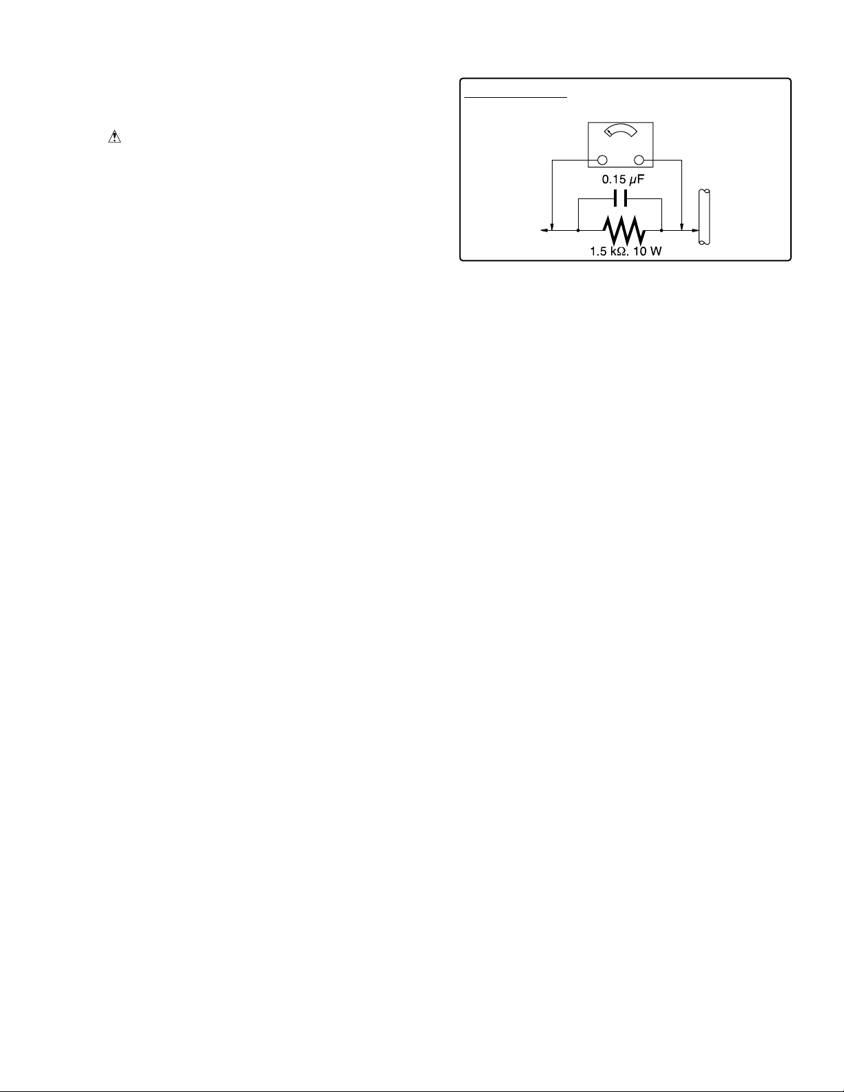
(See figure 1.)
1. Plug the AC cord directly into the AC outlet. Do not use an
2. Connect a 1.5 kΩ, 10 W resistor, in parallel with a 0.15 µF
3. Use an AC voltmeter, with 1 kΩ/V or more sensitivity, to
4. Check each exposed metallic part, and measure the volt-
5. Reverse the AC plug in the AC outlet and repeat each of the
6. The potential at any point should not exceed 0.75 V RMS.
There are special components used in this equipment
which are important for safety. These parts are marked by
in the Schematic Diagrams, Circuit Board Layout,
Exploded Views and Replacement Parts List. It is essential
that these critical parts should be replaced with
manufacturer's specified parts to prevent X-RADIATION,
shock, fire, or other hazards. Do not modify the original
design without permission of manufacturer.
servicing of AC Adaptor whose chassis is not isolated from
the AC power line. Use a transformer of adequate power
rating as this protects the technician from accidents resulting
in personal injury from electrical shocks. It will also protect
AC Adaptor from being damaged by accidental shorting
that may occur during servicing.
short circuit is found, replace all parts which have been
overheated or damaged by the short circuit.
such as insulation barriers, insulation papers shields are
properly installed.
checks to prevent the customer from being exposed to
shock hazards.
prongs on the plug.
the jumpered AC plug and each exposed metallic cabinet
part on the equipment such as screwheads, connectors,
control shafts, etc. When the exposed metallic part has a
return path to the chassis, the reading should be between
1 MΩ and 5.2 MΩ. When the exposed metal does not have
a return path to the chassis, the reading must be infinity.
isolation transformer for this check.
capacitor, between each exposed metallic part on the set
and a good earth ground, as shown in figure 1.
measure the potential across the resistor.
age at each point.
above measurements.
A leakage current tester (Simpson Model 229 or equiva-
lent) may be used to make the hot checks, leakage current
must not exceed 1/2 mA. In case a measurement is outside
of the limits specified, there is a possibility of a shock
hazard, and the equipment should be repaired and rechecked before it is returned to the customer.
Figure. 1
PREVENTION OF ELECTRO
STATIC DISCHARGE (ESD)
TO ELECTROSTATICALLY
SENSITIVE (ES) DEVICES
Some semiconductor (solid state) devices can be damaged
easily by static electricity. Such components commonly are
called Electrostatically Sensitive (ES) Devices. Examples of
typical ES devices are integrated circuits and some field-effect
transistors and semiconductor "chip" components. The following techniques should be used to help reduce the incidence of
component damage caused by electro static discharge (ESD).
1. Immediately before handling any semiconductor component or semiconductor-equipped assembly, drain off any
ESD on your body by touching a known earth ground.
Alternatively, obtain and wear a commercially available
discharging ESD wrist strap, which should be removed for
potential shock reasons prior to applying power to the unit
under test.
2. After removing an electrical assembly equipped with ES
devices, place the assembly on a conductive surface such
as aluminum foil, to prevent electrostatic charge buildup or
exposure of the assembly.
3. Use only a grounded-tip soldering iron to solder or unsolder
ES devices.
4. Use only an antistatic solder removal device. Some solder
removal devices not classified as "antistatic (ESD protected)" can generate electrical charge sufficient to damage ES devices.
5. Do not use freon-propelled chemicals. These can generate
electrical charges sufficient to damage ES devices.
6. Do not remove a replacement ES device from its protective
package until immediately before you are ready to install it.
(Most replacement ES devices are packaged with leads
electrically shorted together by conductive foam, aluminum
foil or comparable conductive material).
7. Immediately before removing the protective material
from the leads of a replacement ES device, touch the
protective material to the chassis or circuit assembly into
which the device will be installed.
CAUTION :
Be sure no power is applied to the chassis or circuit, and
observe all other safety precautions.
8. Minimize bodily motions when handling unpackaged replacement ES devices. (Otherwise harmless motion such
as the brushing together of your clothes fabric or the lifting
of your foot from a carpeted floor can generate static
electricity (ESD) sufficient to damage an ES device).
1-1

X-RADIATION (MODEL: A,
B)
WARNING :
1. The potential source of X-Radiation in EVF sets is the High
Voltage section and the picture tube.
2. When using a picture tube test jig for service, ensure that
jig is capable of handling 10 kV without causing X-Radiation.
NOTE :
It is important to use an accurate periodically calibrated
high voltage meter.
3. Measure the High Voltage. The meter (electrostatic type)
reading should indicate 2.2 kV±0.1 kV. If the meter indication
is out of tolerance, immediate service and correction is
required to prevent the possibility of premature component
failure. To prevent an X-Radiation possibility, it is essential
to use the specified picture tube.
1-2

SERVICE NOTES
NO.
1
2
3
4
PART NUMBER
LSUA0028
LSUA0020
LSUA0019
LSUA0029
PART NAME
32Pin Extension Cable
20Pin Extension Cable
8Pin Extension Cable
40Pin Extension Cable
CONNECTION
FP301 on Main C.B.A. ~ CCD F.P.C. on Lens Unit
FP701 on Main C.B.A. ~ Lens F.P.C. on Lens Unit
FP1 on Main C.B.A. ~ Mechanism Sensor F.P.C. on Mechanism Chassis Ass'y
B2 on Main C.B.A. ~ B3501 on Analog C.B.A.
NO.
5
6
7
8
9
PART NUMBER
VUVS0015
LSUA0017
LSUA0016
LSUA0018
LSUA0020
PART NAME
28Pin Extension Cable
18Pin Extension Cable
10Pin Extension Cable
24Pin Extension Cable
20Pin Extension Cable
CONNECTION
FP7 on Main C.B.A. ~ LCD F.P.C.
FP4 on Main C.B.A. ~ Capstan F.P.C. on Mechanism Chassis Ass’y
FP3 on Main C.B.A. ~ Cylinder F.P.C. on Mechanism Chassis Ass’y
FP5 on Main C.B.A. ~ Head Amp F.P.C. on Mechanism Chassis Ass’y
FP2 on Main C.B.A. ~ Mechanism F.P.C. on Mechanism Chassis Ass’y
EXTENSION CABLES FOR SERVICE POSITION
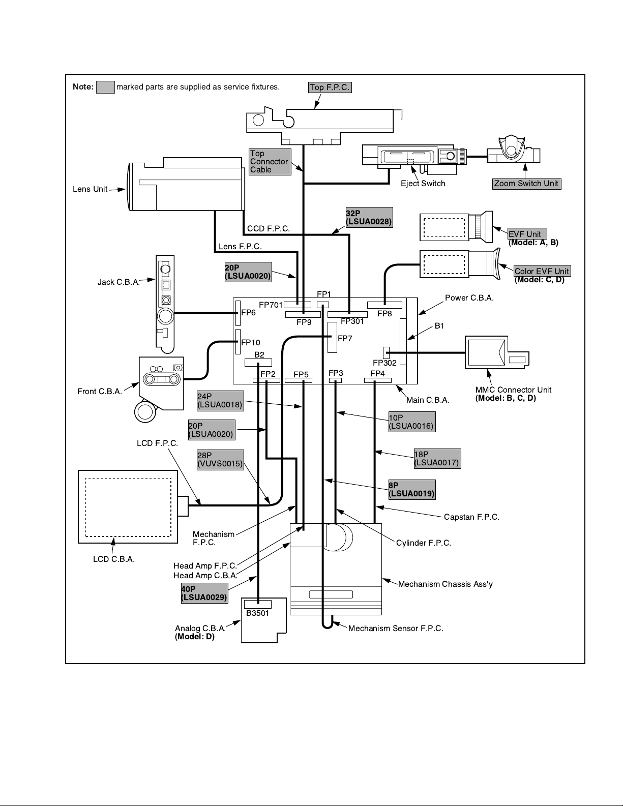
Using the following Extension Cables (No.1 ~ No.4), place the unit as shown for check and service as shown in Fig. 1-1.
Extension Cables (No.5 ~ No.9) are used for improving serviceability as shown in Fig. 1-2. (They are not necessarily used.)
Note :
1. The LCD open/close SW. is for changing between LCD Display or EVF Display. When turning on LCD Display, place some paper
or tape, etc. on LCD open/close SW. so that this SW. stays ON.
2. Use a grounded ESD wrist strap while disassembling the Lens portion.
3. Use extreme care when unplugging or plugging in connectors.
Note: marked parts are supplied as service fixtures.
Lens Unit
Lens F.P.C.
20P
(LSUA0020)
Jack C.B.A.
Front C.B.A.
Note 1
LCD open/close SW.
LCD C.B.A.
Tape
CCD F.P.C.
40P
(LSUA0029)
32P
(LSUA0028)
FP701
FP6
FP9
FP10
B2
FP2
Top F.P.C.
FP1
FP5
Main
C.B.A.
Top Operation Unit
Slide
Eject Switch
FP8
FP7
FP3
FP302
FP4
8P
(LSUA0019)
Mechanism Chassis Ass’y
FP301
B1
Power C.B.A.
Zoom Switch Unit
EVF Unit
(Model: A, B)
Or,
Color EVF Unit
(Model: C, D)
MMC Connector Unit
(Model: B, C, D)
Mechanism Sensor F.P.C.
B3501
Fig. 1-1
1-3
Analog C.B.A.
(Model: D)

Note: marked parts are supplied as service fixtures.
Lens Unit
Lens F.P.C.
20P
(LSUA0020)
32P
(LSUA0028)
24P
(LSUA0018)
28P
(VUVS0015)
20P
(LSUA0020)
Jack C.B.A.
Front C.B.A.
FP6
FP10
B2
FP2
40P
(LSUA0029)
CCD F.P.C.
FP701
FP9
Top F.P.C.
Main
C.B.A.
FP1
FP3
FP5
Eject Switch
Slide
FP4
18P
(LSUA0017)
Top Operation Unit
FP8
FP301
FP7
B1
Power C.B.A.
FP302
Zoom Switch Unit
8P
(LSUA0019)
10P
(LSUA0016)
EVF Unit
(Model: A, B)
Or,
Color EVF Unit
(Model: C, D)
MMC Connector
Unit
(Model: B, C, D)
LCD C.B.A.
LCD F.P.C.
Note 1
LCD open/close SW.
Tape
Head Amp F.P.C.
Cylinder F.P.C.
Mechanism F.P.C.
B3501
Analog C.B.A.
(Model: D)
Fig. 1-2
Head Amp C.B.A.
Mechanism Sensor F.P.C.
Capstan F.P.C.
Mechanism Chassis Ass’y
1-4
INTERCONNECTION OF EXTENSION CABLES
Lens Unit
CCD F.P.C.
Lens F.P.C.
Capstan F.P.C.
Cylinder F.P.C.
Mechanism Sensor F.P.C.
Head Amp F.P.C.
Head Amp C.B.A.
Mechanism
F.P.C.
LCD F.P.C.
LCD C.B.A.
Jack C.B.A.
Front C.B.A.
Mechanism Chassis Ass'y
Main C.B.A.
Power C.B.A.
Analog C.B.A.
(Model: D)
Eject Switch
FP8
B1
FP301
FP1
FP9
FP701
FP6
FP10
B3501
B2
FP2
FP5
FP3
FP4
FP7
FP302
20P
(LSUA0020)
32P
(LSUA0028)
18P
(LSUA0017)
10P
(LSUA0016)
8P
(LSUA0019)
20P
(LSUA0020)
40P
(LSUA0029)
24P
(LSUA0018)
28P
(VUVS0015)
Top F.P.C.
Top
Connector
Cable
Zoom Switch Unit
EVF Unit
(Model: A, B)
Color EVF Unit
(Model: C, D)
MMC Connector Unit
(Model: B, C, D)
Note:
marked parts are supplied as service fixtures.
Fig. 2
1-5
SIMPLIFIED FAULT FINDING DATA (SELF-DIAGNOSTIC SYSTEM)
When following conditions occur, the Power LED will flash according to the condition.
Power LED
CONDITION
T-Reel Lock
S-Reel Lock
Unloading Lock
Loading Lock
Cylinder Lock
Focus Motor Lock
POWER LED FLASHING TIMING & POWER OFF TIMING
After 1 minute flash, power will be turned off.
T = 2.56 sec
0.16 sec
After 1 minute flash, power will be turned off.
After 1 minute flash, power will be turned off.
After 1 minute flash, power will be turned off.
After 1 minute flash, power will be turned off.
Power LED flashes at 1 Hz timing.
Zoom Motor Lock
Dew Detection
Power LED flashes at 1 Hz timing.
After 18 seconds flash at 1 Hz timing, power will be turned off.
Fig. 3
1-6
SHORT JIG C.B.A.
DC Power Supply
(+3 VDC)
"a"
"b"
Loading
Motor
Loading
Posts
CAUTION:
Be sure to attach the Short JIG C.B.A. to protect the
microcontrollers (IC6001 and IC302) after servicing.
(1) Open the LCD Unit.
(2) Remove 2 Screws (A). Then open the Right Cover Unit.
(3) Install the Short JIG C.B.A. to Connector B3.
LCD Unit
B3
direction
Screws (A)
Right Cover
Unit
Fig. 4
Short JIG C.B.A.
METHOD FOR LOADING/UNLOADING OF
MECHANISM
CAUTION:
If loading does not start after DC Power Supply is applied,
DO NOT continue to applying DC Power Supply.
Apply +3 VDC Power Supply to the Loading Motor terminals.
Loading:
DC - to Portion "a," DC + to Portion "b"
Unloading:
DC + to Portion "a," DC - to Portion "b"
Fig. 5
1-7
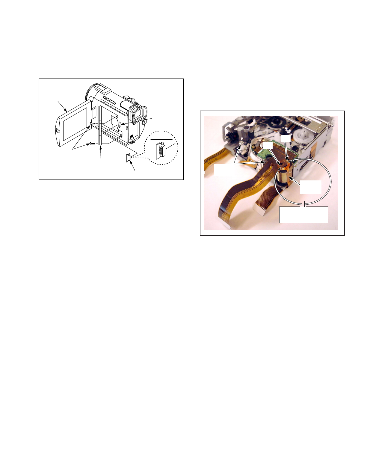
HOW TO REMOVE A JAMMED TAPE
Electrical Method
CAUTION:
If loading does not start after DC Power Supply is applied,
DO NOT continue to applying DC Power Supply. In this
case, perform in Manual Method.
Remove a jammed tape as follows:
(1) Remove the Cabinet Parts. Refer to "CABINET SECTION"
in DISASSEMBLY/ASSEMBLY PROCEDURES.
(2) Apply +3 V DC Power Supply to the Loading Motor terminals.
(3) When the Loading Posts reach the fully unloaded position,
remove the Power Supply immediately.
Note:
DO NOT let eject the Garage Unit. If the Garage Unit is in
the up position, the DV Cassette Tape may be damaged.
Manual Method
(1) Remove the Cabinet Parts. Refer to "CABINET SECTION"
in DISASSEMBLY/ASSEMBLY PROCEDURES.
(2) Remove the Head Amp C.B.A. from Mechanism. Refer to
"MECHANISM SECTION" in DISASSEMBLY/ASSEMBLY
PROCEDURES.
(3) Move the Pinch Roller Unit out so that the Pinch Roller is
separated from the Capstan Rotor Unit shaft. Then, remove
the tape from the tape path and all posts.
"b"
"a"
Loading
Posts
Loading
Motor
DC Power Supply
(+3 VDC)
Fig. 6-1
(4) Rewind the tape into the DV Cassette Tape by turning the
Capstan Rotor clockwise.
Capstan Rotor
Pinch Roller
Capstan Rotor Unit shaft
Top View
(4) Rewind the tape into the DV Cassette Tape by turning the
Capstan Rotor clockwise.
(5) Eject the DV Cassette Tape by sliding the Lock Lever.
Eject Eject
Slide
Move
Tape
Fig. 6-3
Fig. 6-2
(5) Eject the DV Cassette Tape by applying +3 VDC Power
Supply again.
(6) Take out the DV Cassette Tape from the Garage Unit.
Lock Lever
Side View
Fig. 6-4
(6) Take out the DV Cassette Tape from the Garage Unit.
1-8

EEPROM DATA
CAUTION:
Be sure to save the EEPROM data using PC-EVR
Adjustment Program before service and adjustment in
order to make sure to avoid an accidental data loss, etc. as
follows.
There are two EEPROM in this unit.
EEPROM IC
C.B.A.s EEPROM IC Ref. No.
Main C.B.A. (Camera)
Main C.B.A. (Video)
1 How to save the EEPROM data to your PC
1. How to save the EEPROM data for Camera Circuit
1) Start up the PC-EVR Adjustment Program.
2) Select “3. Check [Camera].” in Main menu, and then
press “Enter” key.
3) Select “3. Read (Save)/Write AII EEPROM data” in
Camera check menu, and then press “Enter” key.
4) Select “3. Save all data of EEPROM” in Read (Save)/
Write All EEPROM data menu, and then press “Enter”
key.
5) Input the File name, and then press the “Enter” key. The
data of EEPROM IC will be stored to your PC.
2. How to save the EEPROM data for Video Circuit
1) Start up the PC-EVR Adjustment Program.
2) Select “2. Check [Video].” in Main menu, and then press
“Enter” key.
3) Select “3. Read (Save)/Write All EEPROM data” in
Video check menu, and then press “Enter” key.
4) Select “3. Save all EEPROM data” in Read (Save)/
Write All EEPROM data menu, and then press “Enter”
key.
5) Input the File name, and then press “Enter” key. The
data of EEPROM IC will be stored to your PC.
2 How to write the EEPROM data which was
stored in your PC to EEPROM IC
When it becomes impossible to adjust during service and
adjustment, write the EEPROM data which was stored in
your PC to EEPROM IC as follows. And readjust the
camcorder.
1. How to write the EEPROM data which was stored
for Camera circuit
1) Start up the PC-EVR Adjustment Program.
2) Select “3. Check [Camera].” in Main menu, and then
press “Enter” key.
3) Select “3. Read (Save)/Write AII EEPROM data” in
Camera check menu, and then press “Enter” key.
4) Select “4. Data write using stored file” in Read [Save]/
Write All EEPROM data menu, and then press “Enter”
key.
5) Input the saved file name, and then press “Enter” key.
The data will be written in EEPROM IC.
2. How to write the EEPROM data which was stored
for Video circuit
1) Start up the PC-EVR Adjustment Program.
2) Select “2. Check [Video].” in Main menu, and then press
“Enter” key.
3) Select “3. Read (Save)/Write All EEPROM data” in
Video check menu, and then press “Enter” key.
4) Select “4. Writing from stored data files” in Read (Save)/
Write All EEPROM data menu, and then press “Enter”
key.
5) Input the saved file name, and then press “Enter” key.
The data will be written in EEPROM IC.
IC301
IC6009
3 How to initialize the EEPROM IC
When the EEPROM IC or Main C.B.A. is replaced, be sure
to write the initial data to EEPROM IC. And adjust the
camcorder.
1) Start up the PC-EVR Adjustment Program.
2) Select “3. Check [Camera].” in Main menu, and then
press “Enter” key.
3) Select “3. Read (Save)/Write AII EEPROM data” in
Camera check menu, and then press “Enter” key.
4) Select “4. Data write using stored file” in Read (Save)/
Write All EEPROM data menu, and then press “Enter”
key. Input the saved file name, and then press “Enter”
key.
OR;
Select “5. Data write with initial data,” and then press
“Enter” key. And press “Enter” key once again.
5) Select “2. Check [Video].” in Main menu, and then press
“Enter” key.
6) Select “3. Read (Save)/Write All EEPROM data” in
Video check menu, and then press “Enter” key.
7) Select “4. Writing from stored data files.” in Read
(Save)/Write All EEPROM data menu, and then press
“Enter” key. Input the saved file name, and then press
“Enter” key.
OR;
Select “5. Writing of initial data,” and then press “Enter”
key. And press “Enter” key once again. Then, input ID
Number as follows.
4 How to input ID Number
The ID number is in the EEPROM.
There are two ways to write the data of EEPROM IC after
replacing Main C.B.A. as follows:
• Selecting “4. Writing from stored data files,” ID Number with
stored data file will be written automatically.
• Selecting “5. Writing of initial data,” ID Number needs to be
input. There are two methods, “a” or “b,” to input ID Number
as follows.
a When writing ID Number from the saved data which
is stored in 1-2:
1. Select “2. Check [Video].” in Main menu, and then press
“Enter” key.
2. Select “3. Read (Save)/Write All EEPROM data” in
Video check menu, and then press “Enter” key.
3. Select “6. Writing ID from stored file.” in Read (Save)/
Write All EEPROM data menu, and then press “Enter”
key. Input the saved file name, and then press “Enter”
key. ID Number will be written automatically.
b When the original ID information can not be read
because of destruction of EEPROM etc.:
1. Select “4. Adjust [Video].” in Main menu, and then press
“Enter” key.
2. Select “7. Write products ID” in Video adjustment menu,
and then press “Enter” key. ID Number will be written
automatically.
1-9
HOW TO USE THE DVC HEAD CLEANING TAPE / LSUQ0003
Please use the cleaning tape as described below.
Note: This cleaning tape has a total playback time of 45 minutes. Once used, it is not reusable.
1. Confirm the picture.
NG
2. Playback the cleaning tape for 20 seconds.
3. Confirm the picture again.
NG
4. Playback the cleaning tape for 20 seconds.
5. Confirm the picture again.
NG
6. Playback the cleaning tape for 20 seconds.
7. Confirm the picture again.
NG
8. Replace the Cylinder Unit
OK
The picture will look like this in case of clogged video head.
OK
OK
OK
Playback any normal DVC tape
for 20 minutes or over.
Fig. 7
HOW TO REPLACE THE LAMP (VLLW0023) OF ENHANCEMENT LIGHT UNIT (MODEL: D)
DANGER:
To prevent possible burn hazard, disconnect this unit and
allow lamp to cool before replacing. Replace only with
VLLW0023 lamp, to reduce the risk of fire.
Note :
When installing the Lamp, do not touch the surface of
Lamp directly. Use a clean cloth or tissue to install the
Lamp.
Locking Tabs
Lamp
Screw
Light Case
Locking Tab
1-10
Fig. 8
REPLACEMENT PROCEDURE FOR
MODEL
PV-DV100
PV-DV200
PV-DV400
PV-DV600
NOT USED
A
B
C
D
Z
MARK
Note:
Refer to Item 3 of Schematic Diagram Notes of Schematic
Diagram and Circuit Board Layout Notes, for Mark "Z."
Tweezers
Soldering Iron
Solder
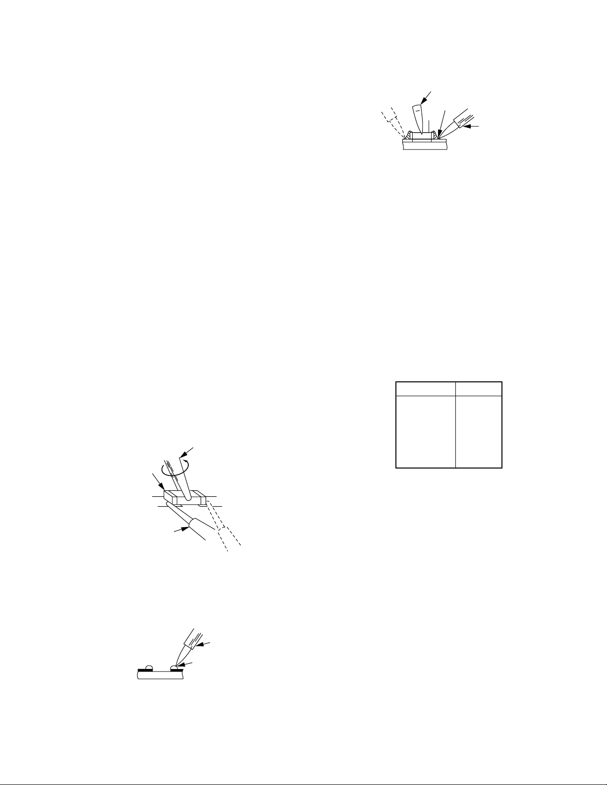
LEADLESS (CHIP) COMPONENT
The following procedures are recommended for the replacement
of the leadless components used in this Unit.
1. Preparation for replacement
a. Soldering Iron
Use a pencil-type soldering iron using less than 30
watts.
b. Solder
Eutectic Solder (Tin 63 %, Lead 37 %) is
recommended.
c. Soldering time
Do not apply heat for more than 4 seconds.
d. Preheating
Leadless capacitor must be preheated before
installation.
(130 °C ~ 150 °C, for about 2 minutes.)
Note:
a. Leadless component must not be reused after removal.
b. Excessive mechanical stress and rubbing of the
component electrode must be avoided.
2. Removing the leadless component
Grasp the leadless component body with tweezers and
alternately apply heat to both electrodes. When the solder
on both electrodes is melted, remove leadless component
with a twisting motion.
Note:
a. Do not attempt to lift the component off the board until
the component is completely disconnected from the
board by a twisting action. The leadless component is
attached to the PCB with glue. So carefully twist the
component when removing it so as not to break or
damage any fail under the component.
b. Take care not to break the copper foil on the printed
board.
b. Press the part downward with tweezers and solder both
electrodes as shown below.
Fig. 9-3
Note:
Do not glue the replacement leadless component to the
circuit board.
SPECIAL NOTE
All integrated circuits and many other semiconductor devices
are electrostatically sensitive and therefore require the special
handlings techniques described under the
"ELECTROSTATICALLY SENSITIVE (ES) DEVICES" section
of this service manual.
MODEL NO. IDENTIFICATION MARK
Use Marks shown in the chart below to distinguish the different
models included in this Service Manual.
Tweezers
Chip
Soldering Iron
Fig. 9-1
3. Installation of the leadless component
a. Presolder the contact points of the circuit board.
Soldering Iron
Presolder
Fig. 9-2
1-11

IC, TRANSISTOR AND CHIP PART INFORMATION
B
E
C
C
E
B
R1
R2
GENERAL C.B.A./ASS'Y PARTS
1
ADM3202ARU, AK4516AVF-E1, AK6480AF-E1,
AN2516S-EV1, AN8021NS-E1, BA6289F-E2,
BA10324AFVE1, BR9040FV-DE2,
LB1837MTEL3, LB1837MLTEL3, LB1837M-TE-L,
LM324DB, M5223FP-720C, M52684BFP,
M62366GP, MM1093NFBE, MN31121SAE1,
NJM2112V-TE1, NJM2115V-TE1,
NJM2151AVTE1, NJM2151V-TE1, NJM2285VTEL1, NJM2407R-TE1, NJM2538VTE2, S29453AFE, S3514AEFSTB, S93C66AMFNTB,
SNLV125APW, SNLV244APW, SNLV4053AFE,
TC7W32FU, TC4W66F, TC4W53FUTEL,
TC90A45F-ELP, UN224-TX, UPD6462GS712,
Z4C2973
MAIN C.B.A.
TSB13LV21GHE MN2MP0006F,
MN103004KBA1
5
4
1
2
3
S814A24AUC
1
2
3
S81333HGKFT1
1
AD80008BUS, AN2109NFHQ,
AN2536FHQ, AN2545FHQ,
AN3742FHN-EB, AN3732FHQ,
BH7086KV, BA9737KV,
F712525APBW, M2-855,
M34521, M5238FP, MN5293-1,
MN102L62GBA, T3W23XB,
TB6534F
E
C
B
2SB1073,
2SB1386T100R,
2SB1386T100Q,
2SD968A
4
3
1
2
PST9328UR
C
B
E
2SD1819, 2SD1819A,
2SC4081T106R, MSB1218A,
2SA1576T106R, 2SB1218A,
2SB1218AI, 2SB1585, 2SB970,
2SA1037K146R, 2SB709A,
2SC3931, 2SK1580, 2SD1119,
2SD2150T100R, 2SD601A,
2SC4617, 2SC2412K1,
2SD2216J, 2SK1958,
2SA1576T106R, 2SC3938,
2SD2436, 2SD1820A, 2SD1328,
2SB1462J, 2SA1774-TLR
1
5
XC6365C503MR,
RN5RG46AATR,
TA75S558FTEL,
NJM2125F-TE2,
NJM2380AFTE1
AC ADAPTOR
4
1
PC357N2N
3
2
UN5114 (R1=10K, R2=47K),
UN5115 (R1=10K, R2=OPEN),
UN9111J (R1=10K, R2=10K),
UN9115J (R1=10K),
DTA114YU (R1=10K, R2=47K),
DTA114TU (R1=10K),
DTA114EE (R1=10K, R2=10K),
DTA114TE (R1=10K),
C
B
E
B
UN2211 (R1=10K, R2=10K),
UN5212 (R1=22K, R2=22K),
UN5213 (R1=47K, R2=47K),
UN9212J (R1=22K, R2=22K),
UN9213J (R1=47K, R2=47K),
DTC144EU (R1=47K, R2=47K),
DTC124EE (R1=22K, R2=22K),
DTC124EU (R1=22K, R2=22K),
DTC144EE (R1=47K, R2=47K)
C
R1
E
R2
CCD C.B.A.
1
MN37290FT
HOW TO READ THE IDENTIFICATION
MARK OF CHIP COMPONENTS.
MARKING PART NO. MARKING PART NO.
B
2SC4081T106R
B 2SB709A
6D UN5114
F
2SA1037L146R
8C UN5213
8B UN5212
6E UN5115
Z 2SD601A
G 2SK1958
Z 2SD1819A
Y 2SD1819
B 2SB1218A
1R 2SB970
U 2SC3931
1X 2SC3938
S 2SC3929
1R 2SB1585
T 2SD1119
MC MA143
1B MA111
1-12
MARKING
BE
UN5212
C
8B
hfe classification
MARKING
C
A
Q
BE
2SB709

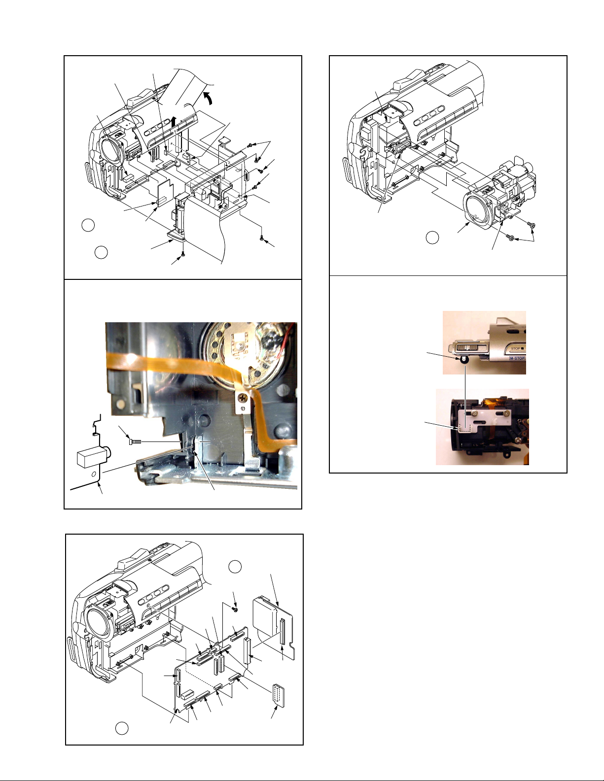
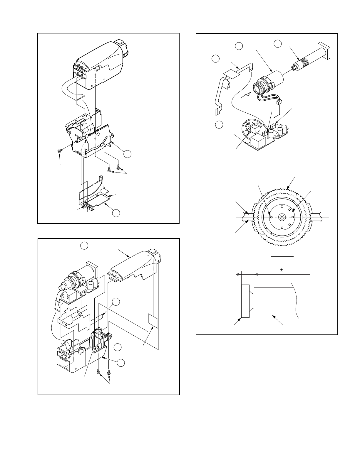
DISASSEMBLY/ASSEMBLY PROCEDURES
CABINET SECTION
Disassembly Flowchart
This flow chart indicates the disassembly steps of the cabinet parts and the P.C.Boards in order to gain access to item (s) to be
serviced. When reassembling, perform the step (s) in the reverse order. Bend, route and dress the wires as they were originally.
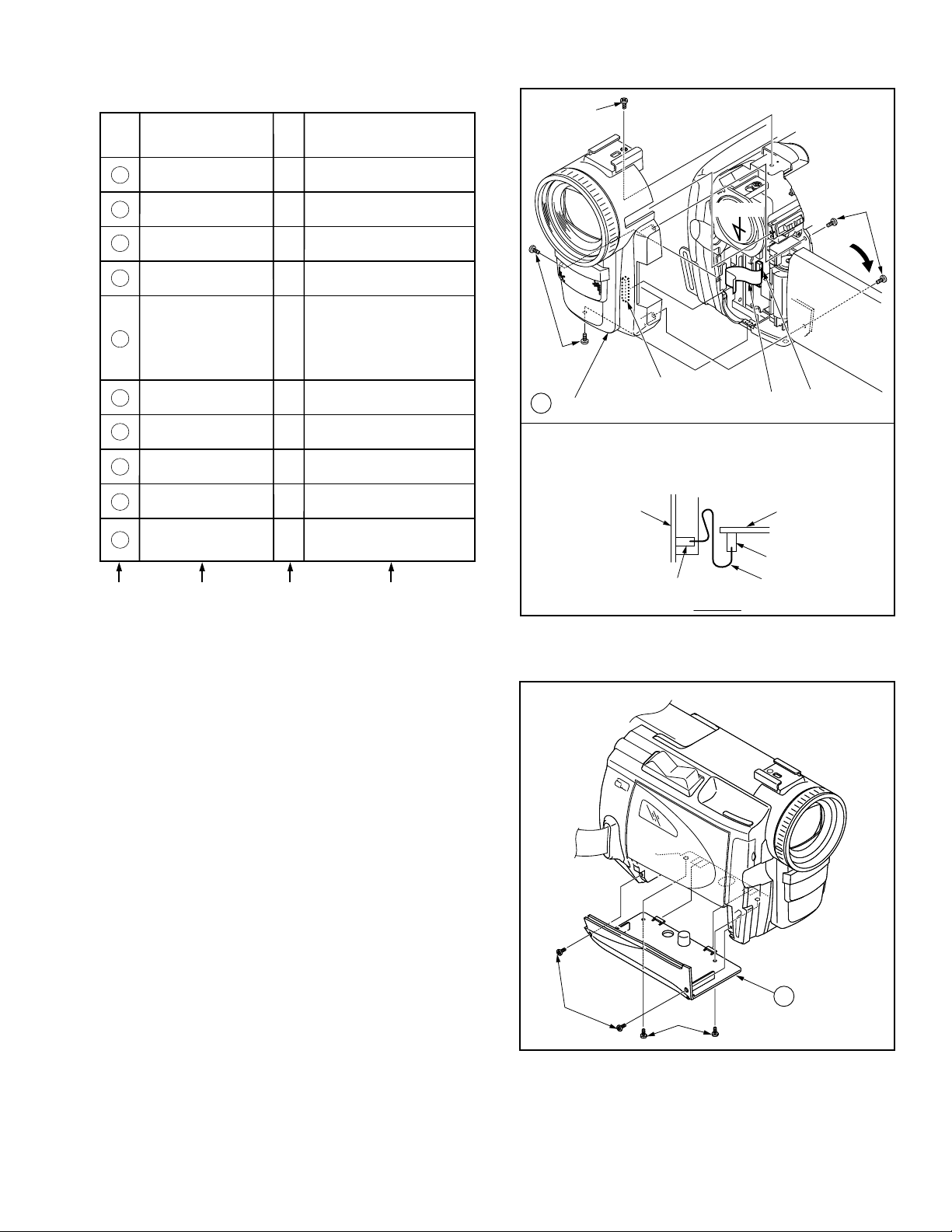
1 Front Case Unit
2 Left Cover
3 Side Case R Unit
4 Analog C.B.A.
(Model: D)
5 Main C.B.A.
6 Power C.B.A.
7 Lens Unit
8 Cassette Cover Unit
9 Mechanism Chassis Ass’y
10 Top Case Ass’y
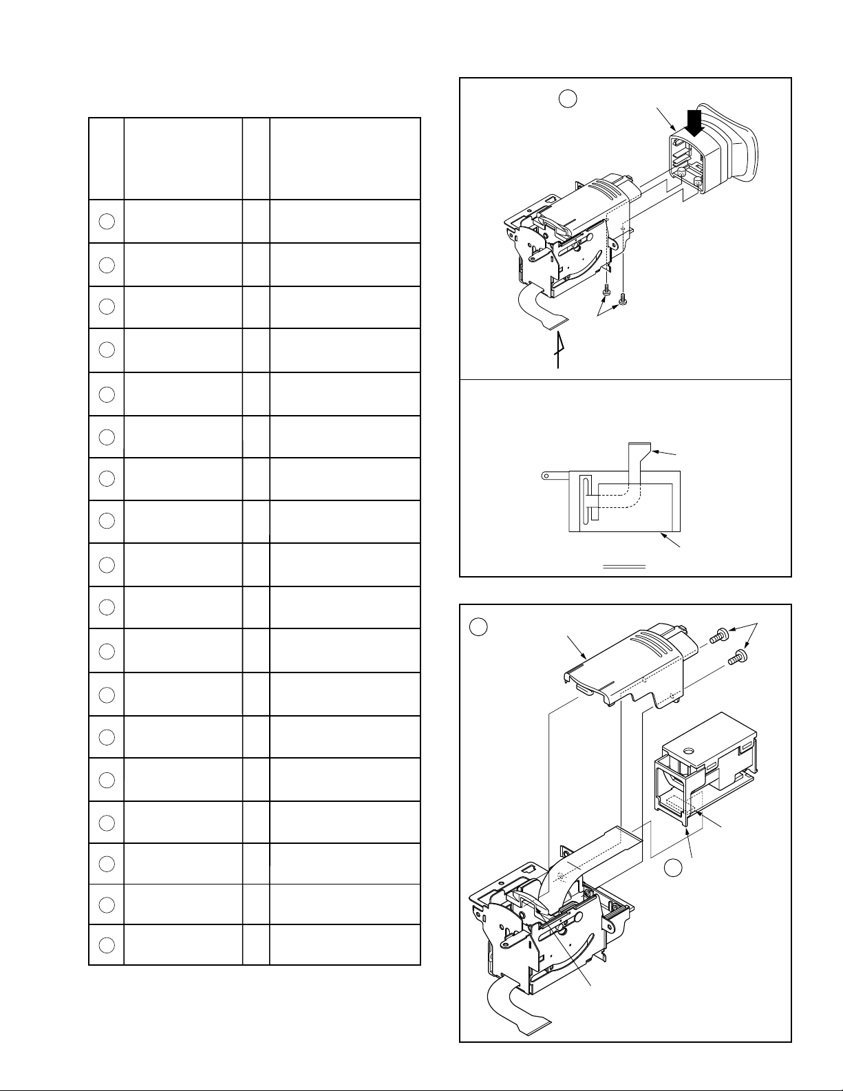
LENS PORTION A
1 CCD C.B.A.
2 Filter Rubber
3 Optical Filter
LENS PORTION B
1 Lens Piece Unit
2 Lens Insulator
3 IR Filter Plate
(Model: C, D)
4 Focus Motor Unit
5 Zoom Motor Unit
FRONT CASE UNIT PORTION
1 Front C.B.A.
2 Shoe
3 Hood Screw
4 IR Panel
(Model: C,D)
SIDE CASE R UNIT PORTION
1 LCD Case Unit
2 Right Cover Unit
3 Speaker Unit
4 Toripod Frame
LCD PORTION
1 LCD Case A Unit
2 LCD Shield Case
3 LCD Shaft Unit
4 LCD Case B
5 LCD C.B.A.
6 LCD Panel Unit
7 LCD Lamp Unit
SIDE CASE L UNIT PORTION
1 Jack Ass’y
2 Strap Angle
3 Jack Cover
4 IN/OUT Knob
5 Jack F.P.C.
6 S-Jack C.B.A.
7 Jack C.B.A.
8 Jack Angle
9 Battery Eject Piece
10 Zoom Switch Unit
11 Hand Strap
TOP CASE UNIT PORTION
1 Top Case Unit
2 Color EVF Unit
or EVF Unit
3 Top Angle
4 Top Connector Cable
5 Top Operation Unit
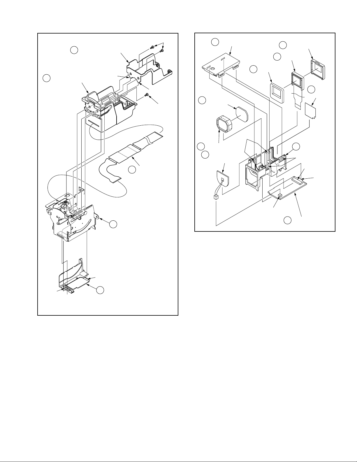
EVF PORTION (Model: A,B)
1 Eye Cap Unit
COLOR EVF PORTION
(Model: C,D)
1 Eye Cap Unit
2 LCD EVF Case A
3 EVF Panel Unit
4 EVF F.P.C. Unit
5 EVF Fixing Angle
6 LCD EVF Case
7 EVF F.P.C.
8 LCD EVF Angle Unit
9 Color EVF A C.B.A.
10 EVF Protect A
11 Protect Plate
12 Color EVF B C.B.A.
13 LED Diffusion Plate
14 LED Lens
15 EVF LCD Holder
16 LCD Panel
17 EVF Rubber
18 EVF Protect B
Fig. D1
2-1
2 EVF Angle Unit
3 EVF F.P.C. Holder
4 EVF Case A Unit
5 Dust Cover
6 EVF ESD Angle Unit
7 EVF Case B
8 EVF F.P.C.
9 CRT
10 Deflection Yoke
11 EVF C.B.A.
Main Parts Portion
STEP
/LOC.
No.
1
PART REMOVE
Front Case Unit D2 3(S-1), 2(S-2), FP4801
Fig.
No.
(S-1)
Left Cover D3 2(S-3), 2(S-4)
2
Side Case R Unit D4
3
Analog C.B.A. D4 B3501
4
Main C.B.A. D5
5
Power C.B.A. D5 B1001
6
Lens Unit D6 2(S-8), (L-1)
7
Cassette Cover
8
Unit
Mechanism Chassis
9
Ass’y
Top Case Ass’y D8
10
5(S-5), (S-6),
FP7, FP302
(S-7),
FP1, FP2, FP3, FP4, FP5,
FP6, FP8, FP9, FP301,
FP701, B3,
Short JIG C.B.A.
D7 ------
D7 3(S-9)
2(S-10), 2(S-11),
Top F.P.C.
A B C D
How to read chart shown above:
A: Order of steps in Procedure
When reassembling, perform the step(s) in the reverse
order. These numbers are also used as the identification
(location) No. of parts in Figures.
B: Part to be removed or installed.
C: Fig. No. showing Procedure or Part Location.
D: Identification of part to be removed, unhooked, unlocked,
released, unplugged, unclamped, or unsoldered.
2(S-1)=2 Screws (S-1), 2(L-1)=2 Locking Tabs (L-1)
View A
(S-2)
Open
(S-1)
FP4801 of Front C.B.A.
1
Front Case Unit
Front
Cable
FP10 of
Main C.B.A.
Reassembly Note:
When installing the Front Case Unit, connect it between
FP10 and FP4801 so that the Front Cable is positioned
correctly as shown.
Front C.B.A.
Main C.B.A.
FP10
FP4801
Front Cable
View A
Fig. D2
Note :
a. When removing the cabinet, work with care so as not to
break the Locking Tabs.
b. Place a cloth or some other soft material under the P.C.
Boards or Unit to prevent damage.
c. When reinstalling, ensure that the connectors are connected
and electrical components have not been damaged.
d. Do not supply power to the unit during disassembly and
reassembly.
2-2
(S-3)
(S-4)
Fig. D3
2
Left Cover
B2
FP7
FP302
(L-1)
up
raise
Power C.B.A.
(S-5)
(S-6)
(S-5)
B3501
Slot A
Analog C.B.A.
4
(Model: D)
3
Side Case
R Unit
(S-5)
(S-5)
Reassembly Note:
When installing the Side Case R Unit, install so that the
Power C.B.A. inserts to the Slot A. Then, tighten Screw
(S-5).
(S-5)
Power C.B.A.
Slot A
Rubber of
IR Filter Knob
(Model: C, D)
7
Lens Unit
Slot of IR Filter Plate
(S-8)
(Model: C, D)
Reassembly Note:
When installing the Lens Unit, install so that the Rubber of
IR Filter Knob inserts to Slot of IR Filter Plate.
Rubber of
IR Filter Knob
(Model: C, D)
Slot of IR
Filter Plate
(Model: C, D)
Fig. D6
FP6
5
Main C.B.A.
Fig. D4
FP9
Fig. D5
FP701
FP1
FP2
B3
FP5
6
Power C.B.A.
(S-7)
FP8
FP4
FP3
Short JIG
C.B.A.
B1
FP301
B1001
2-3

Slot B
Boss A
Slot B
Pin B
8
Cassette Cover Unit
Garage
Boss A
Unit
Pin B
Lock Lever
Slide
Cylinder F.P.C.
Hooking Portion
FRONT CASE UNIT PORTION
STEP
/LOC.
No.
1
2
3
4
PART REMOVE
Front C.B.A.
Shoe
Hood Screw
IR Panel
Fig.
No.
2(S-1)
D9
D10
(S-2)
3(S-3), Lens Ring,
D10
Hood Piece
2(L-1)
D10
9
Mechanism
Chassis Ass’y
Slot A
(S-9)
Slot A
(S-9)
Note:
Remove both the Cassette Cover Unit and the Mechanism
Chassis Ass’y.
Reassembly Note:
(1) Install the Mechanism Chassis Ass’y, and then tighten
3 Screws (S-9).
(2) Eject the Garage Unit by sliding the Lock Lever of
Mechanism Chassis Ass’y.
(3) Install the Cassette Cover Unit so that 2 Slot B are
inserted to 2 Pin B. Then, insert 2 Boss A to 2 Slot A.
Fig. D7
Connector
of Zoom Switch
(S-10)
(S-11)
Unit
Side Case L
Unit
Top F.P.C.
Front Case Unit
Fig. D9
1
Front C.B.A.
(S-1)
(S-11)
Fig. D8
(S-10)
10
Top Case Ass’y
2-4
(L-1)
4
IR Panel
(Model: C, D)
3
Hood Screw
Lens Ring
Front Case
Unit
Hood Piece
Fig. D10
2
Shoe
(S-2)
(S-3)

SIDE CASE R UNIT PORTION
STEP
/LOC.
No.
1
PART REMOVE
LCD Case Unit
Fig.
No.
D11
2(S-1), (L-1), Unsolder
3
Speaker Unit
2
Right Cover Unit
Open
(S-2)
(S-2)
(L-2)
Right Cover Unit 2(S-2), (S-3), 2(L-2)
2
Speaker Unit (S-4)
3
Toripod Frame
4
1
D12
D12
D12
(S-5)
LCD Case Unit
(L-1)
Unsolder
(S-1)
(S-4)
(S-3)
(S-5)
Fig. D12
Boss
4
Toripod Frame
Slot
Slot
Slot
Bosses
Side Case R Unit
Note:
(1)To gain access 2 Screws (S-1), close the LCD Case
Unit, or turn it to the right or left.
(2)Work carefully so as not to damage F.P.C.
Fig. D11
2-5

LCD PORTION
(LCD Case B Unit)
Slots
LCD Case B
4
STEP
/LOC.
No.
LCD Case A Unit
1
2
LCD Shaft Unit
3
LCD Case B
4
LCD C.B.A.
5
LCD Panel Unit
6
LCD Lamp Unit
7
PART REMOVE
LCD Shield Case
Fig.
No.
D14
2(S-1), 6(L-1)
D15
2(S-2)
FP8001
D15
D15
2(S-3)
D16
FP8003, Unsolder
D16
8(L-2)
3(L-3), LCD Sheet Unit
D17
LCD Unit
(S-3)
Case
LCD Shield
2
raise
FP8001
(S-2)
LCD Shaft Unit
3
(S-3)
Note:
When removing the LCD Case B, pull the LCD Unit out of
the slots while raising the lower portion of LCD Unit as
indicated by the arrow.
Fig. D15
(LCD Case Unit)
LCD Case B Unit
Turn
LCD Shaft
Unit
(S-1)
Note:
To gain access to 2 Screws (S-1), turn the LCD Shaft Unit
to the right or left.
Fig. D14
1
LCD Case A Unit
(L-1)
(L-1)
(L-1)
2-6

6
7 LCD Lamp Unit
LCD Lamp Unit
LCD Panel Holder
LCD Panel
Holder
LCD
Reflect
Sheet
LCD Reflect Sheet
Open
Lead Light Panel
(Lead Light Panel Unit)
Lead Light Panel
When installing the LCD Lamp Unit, confirm that the
LCD Lamp Unit is positioned as shown below.
Use extreme care when handling the Lead Light Panel
and the LCD Sheet Unit to avoid damage, dust, and
spots (especially fingerprints, etc.).
Reassembly Note:
(1)
(2)
LCD Sheet
Unit
LCD
Sheet
Unit
(L-3)
(L-3)
View A
View A
LCD Panel Unit
(L-2)
Lead Light Panel Unit
(L-2)
5
(L-2)
LCD C.B.A.
LCD Lamp
Unit
Note:
(1)
When replacing the Lead Light Panel Unit, make sure
to remove Protection Sheet as shown below.
(2)
Use extreme care when handling the Lead Light Panel
Unit and the LCD Panel Unit to avoid damage, dust,
and spots (especially fingerprints, etc.).
The use of clean cotton gloves when available is
highly recommended.
Be careful not to apply any pressure to Portion "a" and
(3)
"b" of the LCD Lamp Unit as shown below.
Portion "a"
After replacing the Lead Light Panel Unit, confirm
(4)
that the Terminal of LCD Lamp Unit is soldered
correctly as shown below.
(L-2)
LCD Lamp Unit
Lead Light Panel Unit
Solder
Unsolder
FP8003
Unsolder
Portion "b"
Protection Sheet
Fig. D17
LCD C.B.A.
Hole of
Lead Light
Panel Unit
1~1.4mm
Fig. D16
Terminal of
LCD Lamp Unit
2-7

LENS PORTION A
Optical
Filter
Filter
Rubber
Filter
Rubber
View B
View B
CCD
Surface
Plate
CCD
F.P.C.
Hole
(B)
Hole
(B)
Hole (A)
Hole (A)
CCD
CCD
CCD
C.B.A.
Thinnest layer
(Model: A, B)
(Model: C, D)
Lens
Unit
(S-1)
Lens
Unit
Note:
This Optical Filter
is reversible to use.
Reassembly Note:
1. Installation of the Optical Filter
(1) Install the Optical Filter in the Lens Unit correctly.
Note:
(Model: A, B)
Be sure to install the Optical Filter with the thinnest
layer of the Optical Filter facing toward the Lens Unit.
Make sure that no dust gets on the Optical Filter and
in the Lens Unit. Clean the Optical Filter with lens
cleaning paper dampened with lens cleaner if
necessary.
2. Installation of the Filter Rubber
(1) Install the Filter Rubber in the Lens Unit correctly as
shown bellow.
Note:
Make sure that no dust gets on the Filter Rubber.
3. Installation of the CCD C.B.A.
(1) Place the CCD Surface Plate so that Holes (A) are
aligned with Holes (B) on the CCD F.P.C.
(2) Carefully install the CCD onto the CCD F.P.C. by
soldering.
Note:
Do not apply heat to the CCD directly when soldering.
Keep soldering time to a minimum to prevent damage
to the CCD.
Install the CCD and CCD Surface Plate so that there
are no gaps between them.
When installing, do not touch the CCD window surface
and make sure that no dust gets on the CCD. Clean
the CCD window surface with lens cleaning paper
dampened with lens cleaner if necessary.
(3) Install the CCD C.B.A. to the Lens Unit. Then, secure
2 Screws (S-1) while keeping the CCD C.B.A. pressed
toward the upper right corner.
Solder
STEP
/LOC.
No.
1
2
3
PART
CCD C.B.A.
Filter Rubber
Optical Filter
Fig.
No.
D18
D18
D18
2(S-1)
-----
-----
Lens Unit
Optical Filter
3
Filter Rubber
2
CCD
CCD
Pin
1
CCD
C.B.A.
Unsolder
Note:
1. Removal of the CCD and the CCD Surface Plate
(1) Unsolder the CCD Pins on the CCD F.P.C.
(2) Remove the CCD and the CCD Surface Plate from the
(S-1)
CCD F.P.C.
CAUTION:
(1) When removing the CCD C.B.A., take care so that the
Optical Filter does not fall out.
(2) Take extreme care when removing the CCD because
it is easily damaged by static electricity.
Use a Wrist Strap while removing and installing.
(3) Do not apply heat to the CCD directly when soldering.
Keep soldering time to a minimum to prevent damage
to the CCD.
(4) Do not touch the CCD window surface when servicing.
Fig. D18
REMOVE
CCD
Surface
Plate
CCD
F.P.C.
Fig. D19
2-8

LENS PORTION B
STEP
/LOC.
No.
1
PART REMOVE
Lens Piece Unit
Fig.
No.
D20
3(S-1)
5
Zoom Motor Unit
(S-3)
Unsolder
Portion A
4
Focus
Motor
Unit
Holder
Slots of Holder
Lens Insulator -----
2
IR Filter Plate 2(S-2)
3
Focus Motor Unit
4
5
D20
D20
D21
D21
2 Lens Insulator
(S-1)
(S-1)
1
Lens Piece
Unit
3 IR Filter Plate
2(S-3), Unsolder
2(S-4), UnsolderZoom Motor Unit
Lens Unit
(Model: C, D)
Pin of IR
Lever
(Model: C,D)
Slot
(S-2)
(S-4)
View A
Unsolder
Reassembly Note:
When installing the Zoom Motor Unit, install so that the
Portion A of Zoom Motor Unit is inserted to Slots of Holder
by sliding the Holder.
Slide
Slots of
Holder
Holder
View A
Fig. D21
Note:
When installing the IR Filter Plate, install so that the Pin of
IR Lever is inserted to Slot of IR Filter Plate. After installing,
confirm that the IR Filter Plate and IR Lever are slide correctly.
Fig. D20
2-9
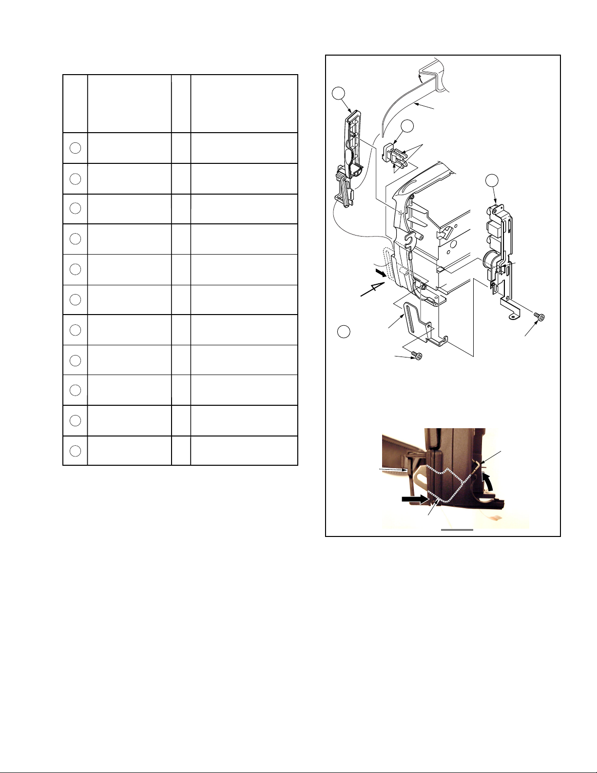
SIDE CASE L UNIT PORTION
STEP
/LOC.
No.
PART REMOVE
Fig.
No.
3
Jack Cover
Open
Hand Strap
4
IN/OUT Knob (Model: D)
Jack Ass’y
1
Strap Angle (S-2)
2
Jack Cover Hand Strap
3
IN/OUT Knob
4
5
6
7
8
9
10
D22
D22
D22
D22
D23
D23
D23
D23
D24
D24
(S-1)
2(L-1)
FP3701, FP3751Jack F.P.C.
(S-3)S-Jack C.B.A.
(S-4)Jack C.B.A.
-----Jack Angle
(S-5)Battery Eject Piece
2(S-6)Zoom Switch Unit
(L-1)
1
Jack Ass'y
IN/OUT
Push
Switch
(Model: D)
View A
2
Strap Angle
(S-1)
(S-2)
Note:
When removing the Strap Angle, push Strap Angle lower
portion to release as shown.
DO NOT remove the Jack Cover before removing the Strap
Angle.
11
D24
-----Hand Strap
Strap Angle
Jack Cover
Push
lower portion
View A
Fig. D22
2-10

8
Jack Angle
7
Jack C.B.A.
10
Zoom Switch Unit
(S-6)
(S-6)
Eject Plate
6
S-Jack C.B.A.
(S-3)
FP3751
Fig. D23
hole
5
Jack F.P.C.
(S-4)
FP3701
Portion A
Eject Knob Piece
Tab of Switch
(Model: B,C,D)
(S-5)
Portion B
9
Battery Eject
Piece
Slot of MMC Exchange Knob
(Model: B, C, D)
11
Hand Strap
Eject Knob Piece
Bosses
Eject Plate
Note: Work carefully so as not to damage the F.P.C.
Reassembly Note:
(1) When installing the Zoom Switch Unit, install Portion B
after installing Portion A.
(2) When installing Portion B, install so that the Tab of
Switch inserts to Slot of MMC Exchange Knob.
Slot of MMC
Exchange Knob
(Model: B, C, D)
Tab of Switch
(Model: B,C,D)
Fig. D24
2-11
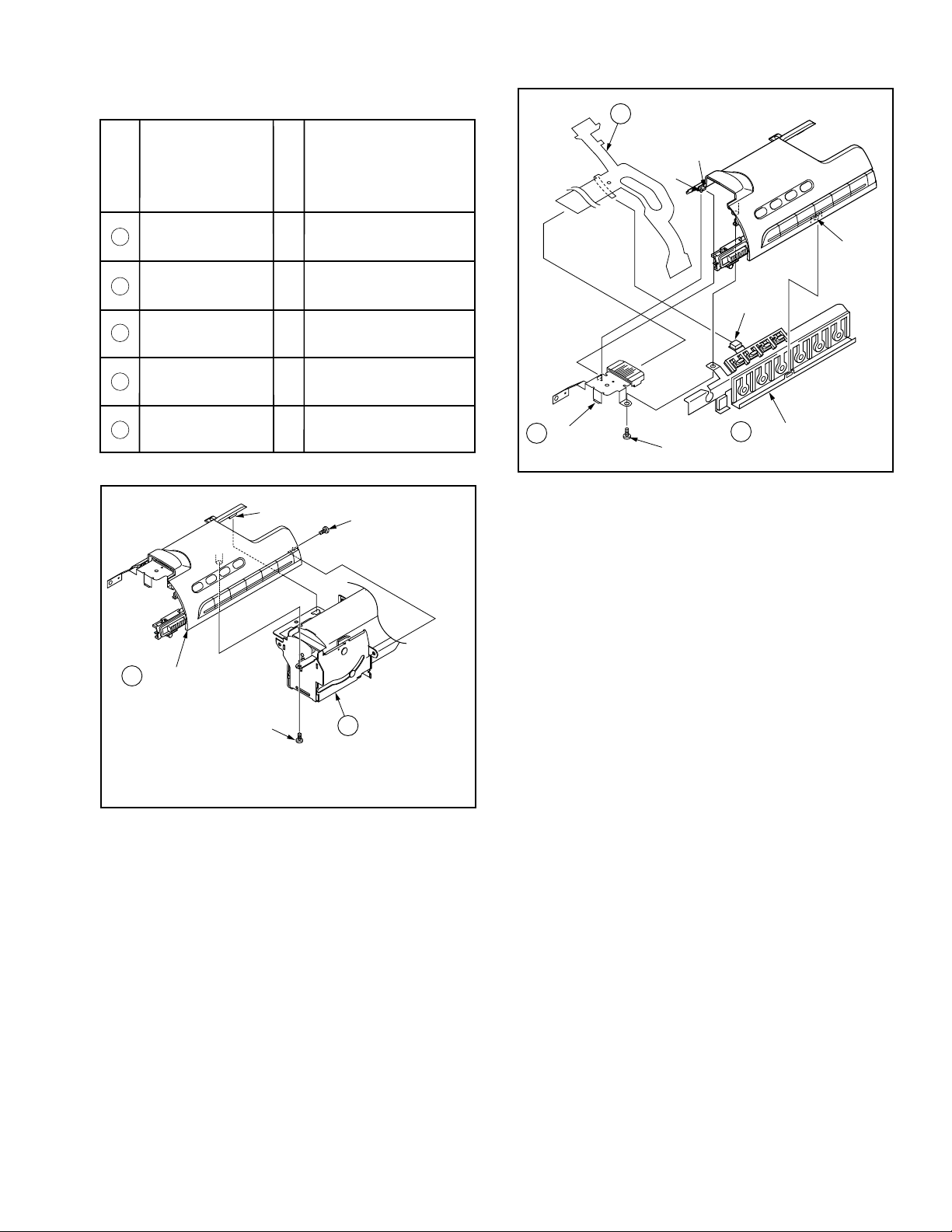
TOP CASE UNIT PORTION
4
Top Connector Cable
STEP
/LOC.
No.
1
2
3
4
PART REMOVE
Top Case Unit
Color EVF Unit
or EVF Unit
Top Angle (S-3), (L-2)
Top Connector Cable
5
Fig.
No.
D25
D25
D26
D26
D26
(L-1)
(S-1), (S-2), (L-1)
-----
Connector
(L-3)Top Operation Unit
(S-2)
3
Top Angle
Boss
(S-3)
(L-2)
Connector
Fig. D26
5
Top Operation Unit
(L-3)
1
Top Case Unit
(S-1)
Fig. D25
2
Color EVF Unit
(Model: C, D)
or
EVF Unit
(Model: A, B)
2-12
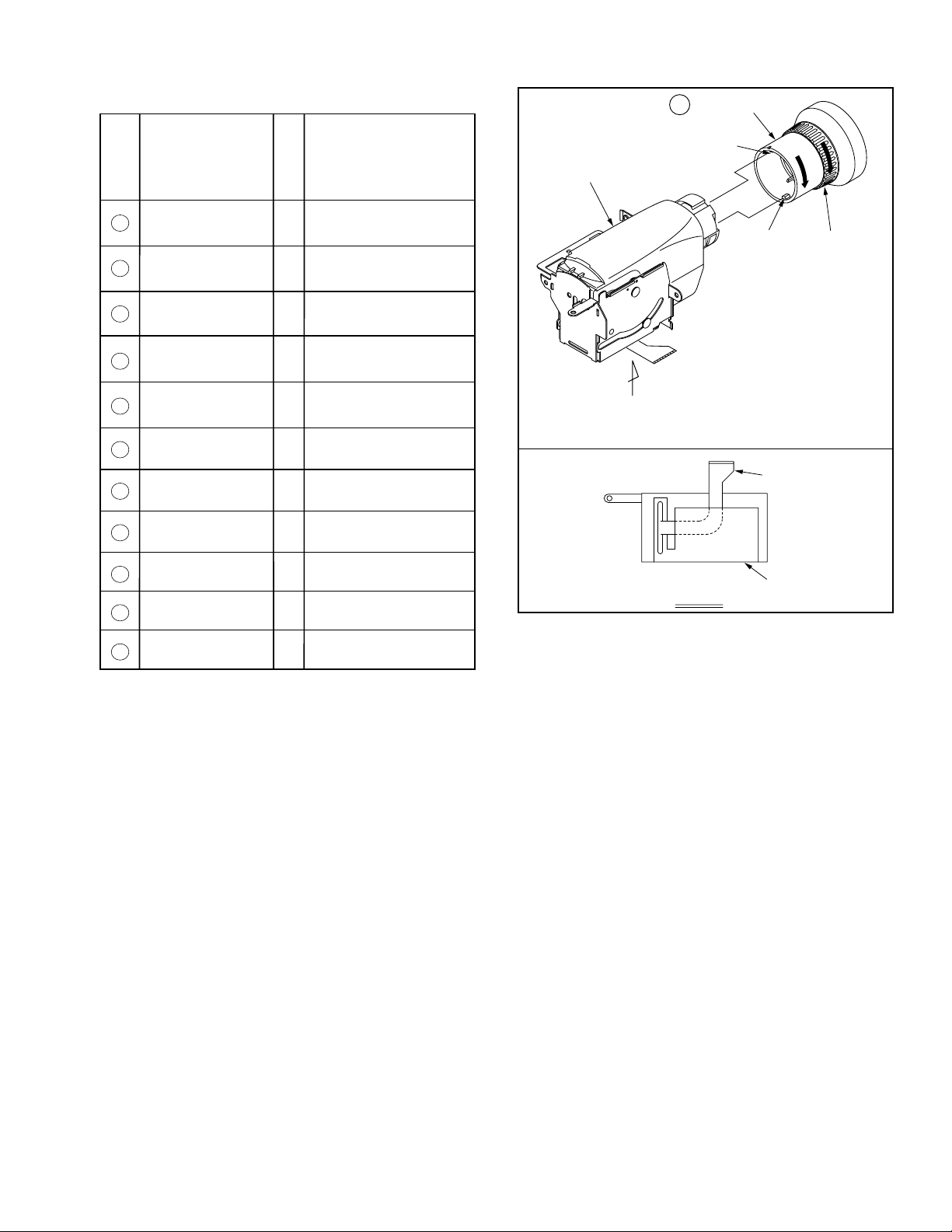
EVF UNIT PORTION (Model: A, B)
1
Eye Cap Unit
STEP
/LOC.
No.
1
2
3
4
5
6
7
8
9
10
11
PART REMOVE
Eye Cap Unit
EVF Angle Unit (S-1), 2(S-2)
EVF F.P.C. Holder
EVF Case A Unit 2(S-3)
Dust Cover -----
EVF ESD Angle Unit -----
EVF Case B (L-3)
EVF F.P.C. FP801
CRT -----
Deflection Yoke P902, CRT Socket Unit
EVF C.B.A. -----
Fig.
No.
D27
D28
D28
D29
D29
D29
D29
D30
D30
D30
D30
2(L-1)
2(L-2)
(L-1)
Turn
EVF Case Unit
(L-1)
Eye Sight RIng
View A
Note:
The Eye Cap Unit is very tight. Use extreme so as not to
damage the unit.
EVF F.P.C.
EVF F.P.C. Holder
View A
Fig. D27
Note:
When disassembling or reassembling, make sure that no dust
gets in EVF Unit.
2-13
8
EVF F.P.C.
10
Deflection
Yoke
9
CRT
(S-1)
(L-2)
Fig. D28
4
EVF Case A Unit
2
EVF Angle Unit
(S-2)
(L-2)
3
EVF F.P.C. Holder
View A
11
EVF
C.B.A.
CRT
Socket
Unit
Lead (YELLOW)
Lead (BLUE)
FP801
Anode Pin
5.35 mm 1.35 mm
P902
Deflection Yoke
CRT
View "A"
(L-3)
(S-3)
Fig. D29
6
EVF ESD
Angle Unit
5
Dust Cover
7
EVF Case B
2-14
CRT
Deflection Yoke
Fig. D30
COLOR EVF UNIT PORTION (Model: C,
D)
1
Eye Cap Unit
Push
STEP
/LOC.
No.
1
2
3
4
5
6
7
8
PART REMOVE
Eye Cap Unit
LCD EVF Case A 2(S-2)
EVF Panel Unit FP901
EVF F.P.C. Holder
EVF Fixing Angle 3(S-3), 2(L-2)
LCD EVF Case -----
EVF F.P.C. -----
LCD EVF Angle Unit -----
Fig.
No.
D31
D32
D32
D33
D33
D33
D33
D33
2(S-1)
(S-1)
2(L-1)
View A
Reassembly Notes:
When installing the Eye Cap Unit, tighten 2 Screws (S-1)
while pushing as indicated by the arrow.
EVF F.P.C.
Color EVF A C.B.A. (L-3), P901, FP902
9
EVF Protect A 4(L-4)
10
Protect Plate -----
11
Color EVF B C.B.A. -----
12
LED Diffusion Plate -----
13
LED Lens -----
14
EVF LCD Holder -----
15
LCD Panel -----
16
EVF Rubber -----
17
EVF Protect B -----
18
D34
D34
D34
D34
D34
D34
D34
D34
D34
D34
2
LCD EVF Case A
View A
Fig. D31
EVF F.P.C. Holder
FP901
3
EVF Panel Unit
(S-2)
Note:
When disassembling or reassembling, make sure that no dust
gets in Color EVF Unit.
2-15
hole
Fig. D32
6
LCD EVF Case
5
EVF Fixing Angle
(L-2)
(L-2)
(S-3)
(S-3)
10
EVF Protect A
13
LED Diffusion
Plate
17
(L-4)
15
16
LCD Panel
EVF Rubber
EVF LCD Holder
11
Protect
Plate
7
EVF F.P.C.
8
LCD EVF Angle Unit
(L-1)
4
(L-1)
Note:
Work carefully so as not to damage the F.P.C.
EVF F.P.C. Holder
14
LED Lens
12
Color EVF B
C.B.A.
P901
Fig. D34
18
EVF
Protect B
(L-4)
FP902
9
Color EVF A
C.B.A.
(L-3)
Fig. D33
2-16
 Loading...