Panasonic PNA2602M Datasheet

Darlington Phototransistors
PNA2602M
Darlington Phototransistor
For optical control systems
Features
Darlington output, high sensitivity
Easy to combine light emission and photodetection on same
printed circuit board
Small size, thin side-view type package
Long lead and visible light cutoff design with PN205
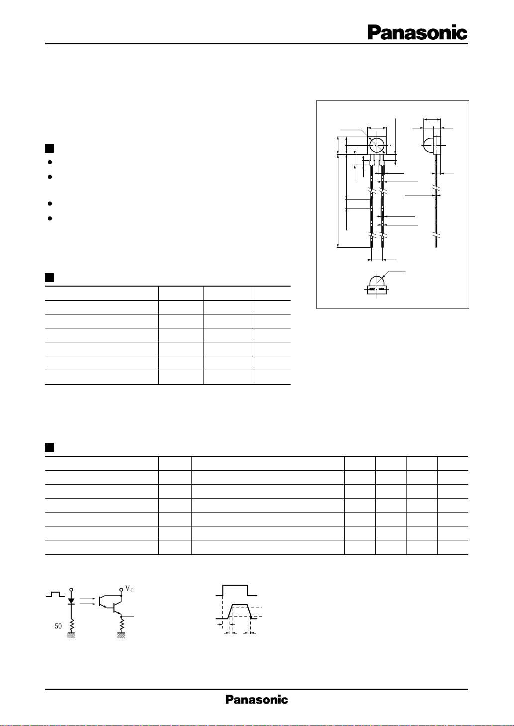
Absolute Maximum Ratings (Ta = 25˚C)
Parameter Symbol Ratings Unit
Collector to emitter voltage
Emitter to collector voltage
Collector current I
Collector power dissipation
Operating ambient temperature
Storage temperature T
V
CEO
V
ECO
C
P
C
T
opr
stg
20 V
5V
30 mA
100 mW
–25 to +80 ˚C
–30 to +100 ˚C
ø3.5±0.2
2.4
4.8±0.336.6±0.5
2.414.52.2±0.2
2.95
1.0
4.5±0.3
12
Not soldered
2-1.12
2-0.45±0.15
2-0.6±0.15
2-0.45±0.15
2.54
R1.75
4.2±0.3
2-0.4±0.15
Unit : mm
1.92.3
1.2
1: Emitter
2: Collector
Electro-Optical Characteristics (Ta = 25˚C)
Parameter Symbol Conditions min typ max Unit
Dark current I
Sensitivity to infrared emitters
CEO
S
Peak sensitivity wavelength
Acceptance half angle θ
Response time tr, t
Collector saturation voltage
*1
Measurements were made using infrared light (λ = 940 nm) as a light source.
*2
Switching time measurement circuit
Sig.IN
50Ω
V
R
CC
Sig.OUT
L
V
CE(sat)
(Input pulse)
(Output pulse)
VCE = 10V 0.5 µA
*1
VCE = 10V, H = 3.75 µW/cm
IR
λ
VCE = 10V 850 nm
P
Measured from the optical axis to the half power point
*2
VCC = 10V, IC = 1mA, RL = 100Ω 150 µs
f
*1
IC = 100µA, H = 3.75 µW/cm
90%
t
d
t
r
10%
t
f
2
0.1 3.0 mA
35 deg.
2
t
: Delay time
d
: Rise time (Time required for the collector photo current to
t
r
increase from 10% to 90% of its final value)
: Fall time (Time required for the collector photo current to
t
f
decrease from 90% to 10% of its initial value)
1.5 V
1

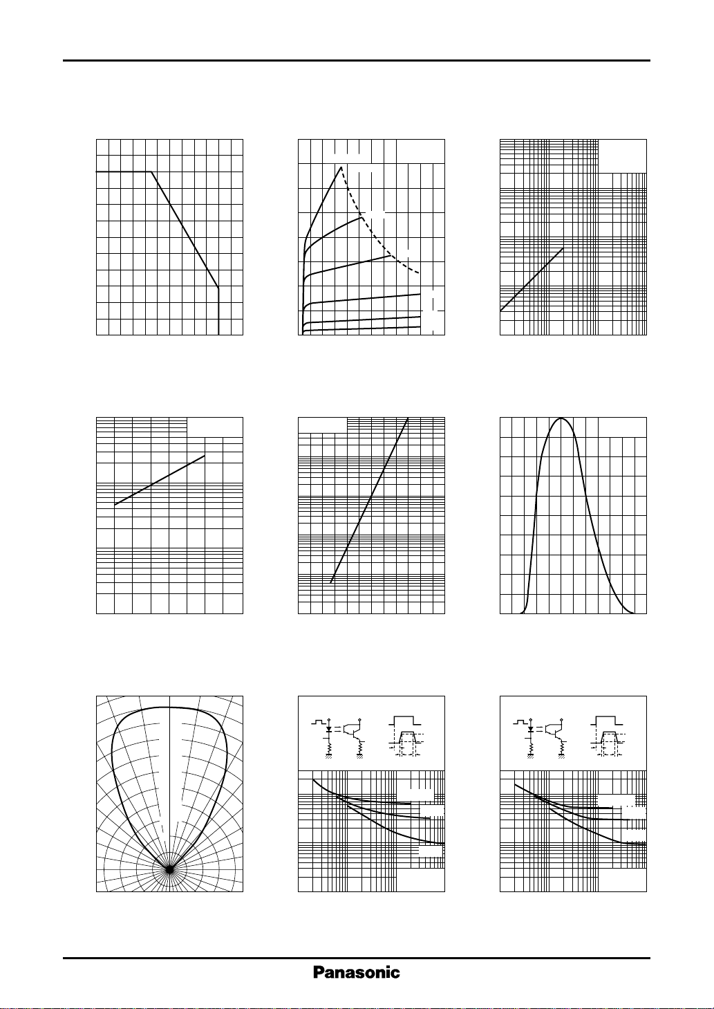
PNA2602M Darlington Phototransistors
P
— Ta
120
100
(mW)
C
80
60
40
20
Collector power dissipation P
0
– 20
C
0 20406080100
Ambient temperature Ta (˚C )
I
— Ta
10
CE(L)
(mA)
1
CE(L)
VCE = 10V
T = 2856K
I
— V
16
PC = 100mW
L = 50 lx
(mA)
12
CE(L)
8
4
Collector photo current I
0
02016812424
CE(L)
30 lx
CE
Ta = 25˚C
T = 2856K
20 lx
10 lx
5 lx
2 lx
3
10
2
(mA)
10
CE(L)
10
1
Collector photo current I
–1
10
1
Collector to emitter voltage VCE (V)
I
— Ta
2
10
10
(µA)
1
CEO
CEO
VCE = 10V
Spectral sensitivity characteristics
100
80
60
I
— L
CE(L)
10 10
2
Illuminance L (lx)
V
= 10V
CE
Ta = 25˚C
T = 2856K
V
= 10V
CE
Ta = 25˚C
3
10
–1
10
Collector photo current I
–2
10
– 40 0 40 80 120
Ambient temperature Ta (˚C )
Directivity characteristics
0˚ 10˚ 20˚
100
90
80
70
60
50
40
Relative sensitivity S (%)
30
20
30˚
40˚
50˚
60˚
70˚
80˚
90˚
–1
10
Dark current I
–2
10
–3
10
– 20 0 40 8020 60 100
Ambient temperature Ta (˚C )
t
— I
r
CE(L)
Sig.IN
Sig.
OUT
50Ω
(µs)
r
3
10
V
CC
Sig.
OUT
t
L
d
trt
RL = 1kΩ
R
Rise time t
2
10
VCC = 10V
10
–2
10
–1
10
Collector photo current I
Ta = 25˚C
110
CE(L)
90%
10%
f
500Ω
100Ω
(mA)
40
Relative sensitivity S (%)
20
0
700 800 900 1000 1100 1200
600
Wavelength λ (nm)
t
— I
f
Sig.IN
Sig.
OUT
50Ω
(µs)
f
3
10
V
CC
Sig.
OUT
R
L
Fall time t
2
10
10
–2
10
–1
10
Collector photo current I
CE(L)
90%
10%
t
d
t
rtf
RL = 1kΩ
500Ω
100Ω
VCC = 10V
Ta = 25˚C
110
(mA)
CE(L)
2
 Loading...