

http://cxema.ru
ORDER NO. VRD0102006C2
Video Cassette Recorder
NV-FJ621EG / NV-FJ621EGY / NV-FJ621B / NV-FJ621EC /
NV-FJ621ECM / NV-FJ621ECN / NV-FJ621ECY
Z-MECHANISM
SPECIFICATIONS
© 2001 Matsushita Electric Industrial Co., Ltd. All rights reserved. Unauthorized copying and distribution is a violation of
law.

http://cxema.ru
1. INTRODUCTION
This service manual contains technical information which will allow service personnel to understand and
service this model.
If the circuit is changed or modified, this information will be followed by supplementary service manual to be
filed with original service manual.
Note:
1. Adjustment procedures, Disassembly Procedures and Assembly Procedures for Mechanism Chassis are separate
volume from this service manual. / Please refer to the service manual for Z-Mechanism Chassis. (Order No.
VRD9802005C2)
2. The Model No. is indicated on the Schematic Diagram and Circuit Board Diagrams as follows.
Model No. Indication Mark
NV-FJ621EG (A)
NV-FJ621EGY (B)
NV-FJ621B (C)
—————— (D)
NV-FJ621EC/ECM/ECN (E)
NV-FJ621ECY (F)
2. GENERAL DESCRIPTIONS
2.1. SERVICE CAUTION
2.1.1. REPLACING IC7702/EEPROM
When the EEPROM: IC7702 is replaced, applicable model code, option code and electrical adjustment data
will not be available.
Therefore, enter and/or adjust the necessary data after replacing IC7702 by referring following procedure.
STEP1.REPLACE THE IC7702
1. Remove the C.B.A. with Mechanism unit by referring the Disassembly procedure.
2. Disconnect the AC plug and replace the IC7702.
STEP2.INPUT THE MODEL & OPTION CODE
1. Set up the applicable model code and option code by ordering the following table.
http://cxema.ru
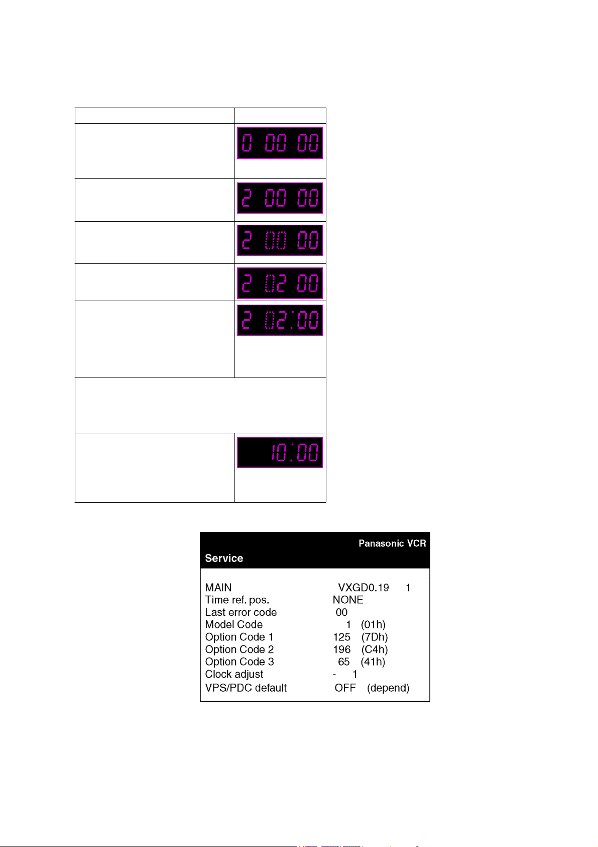
PROCEDURE F.I.P. DISPLAY
Turn on the Service Mode
1.Press the FF key and the
EJECT key simultaneously for
more than 3 seconds.
Activate the Service Mode 2
2.While keep placing FF key,
press the EJECT key in twice.
Activate the Entering Mode.
3.Press the EJECT key for more
than 3 seconds.
Set the Mode 2.
4.Press the CH UP key in twice.
Display the Setting Code.
5.Press the POWER Button to
turn the power on.
Enter the Model and Option Code.
6.Set the applicable Model and Option code by using
REW, PLAY, STOP and FF keys on the Remote
Controller. (See Fig.S1 & S2)
Exit from Service Mode.
7.Press the POWER Button to
turn the power off.
8. Press FF and EJECT keys
simultaneously in 6 times.
(Colon starts
flashing)
(Normal Indication)
Fig.S1 Service Secreen (sample)
http://cxema.ru
Model No. Model
Code
NV-FJ621EG/
81 / (51h) 8 / (08h) 212 /
/ EGY
NV-FJ621EC/
82 / (52h) 8 / (08h) 212 /
/
Option
Code 1
Option
Code 2
(D4h)
(D4h)
Option
Code 3
6 / (06h)
6 / (06h)
ECM/ECN/ECY
NV-FJ621B 83 / (53h) 40 / (28h) 212 /
5 / (05h)
(D4h)
Fig. S2 Model Code & Option Code
NOTE:
Since all electrical adjustments data is still not available, perform the Electrical Adjustment continuously.
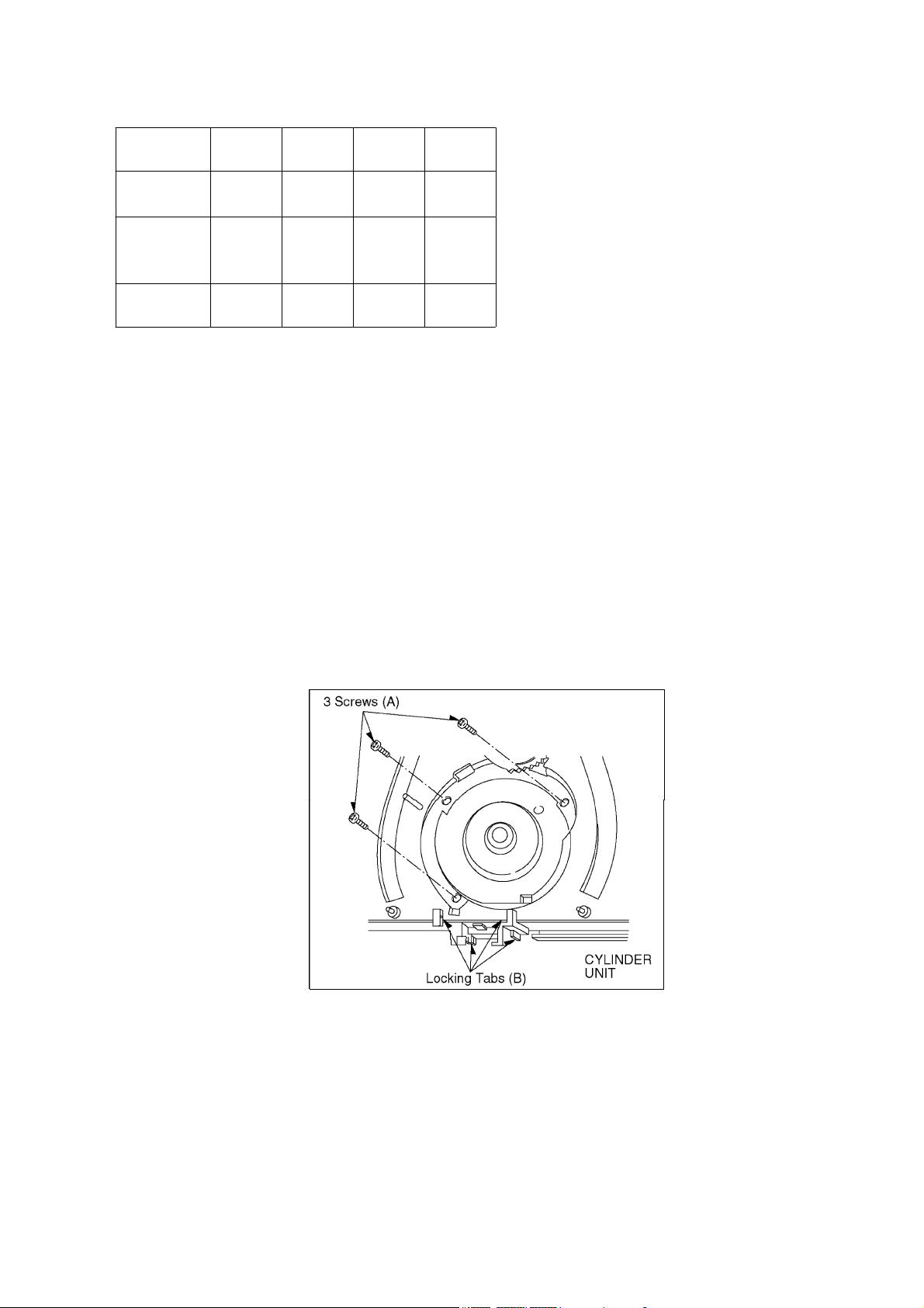
2.1.2. CYLINDER UNIT REPLACEMENT
1. CYLINDER UNIT REPLACEMENT
A. Remove the mechanism unit from MAIN C.B.A./Chassis by referring “SECTION 2. Disassembly Procedure”.
B. Remove the 3 screws (A) of the CYLINDER UNIT with a screw driver.
C. Unlock the 4 locking tabs (B) and disconnect the Cylinder fiexible card from the FPC Holder.
D. Remove the CYLINDER UNIT.
CAUTION:
Handle the Cylinder fiexible card with care. When it damaged, you should replace whole Cylinder unit.
Fig. S3
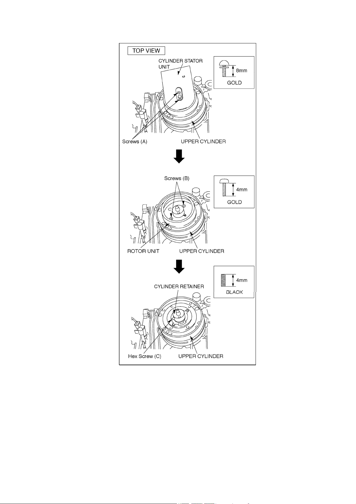
2. UPPER CYLINDER DISASSEMBLY
A. Remove 2 screws (A).
B. Remove the Cylinder Stator Unit.
C. Remove 2 screws (B).
D. Remove the Cylinder Rotor Unit.
E. Loose Hex screw (C) (1.5 mm) and remove the CYLINDER RETAINER.
F. Remove the Upper Cylinder.
Fig. S4
http://cxema.ru
3. UPPER CYLINDER ASSEMBLY
When reassembling, perform the steps in the reverse order.
Notes:
1. Install the Cylinder Retainer so that the 2 holes on top of the Cylinder Retainer are at right angles with the P3502
Connection.
2. Tighten the Hex screw (C) (1.5 mm) while pressing down on top of the Cylinder Retainer.
Fig. S5
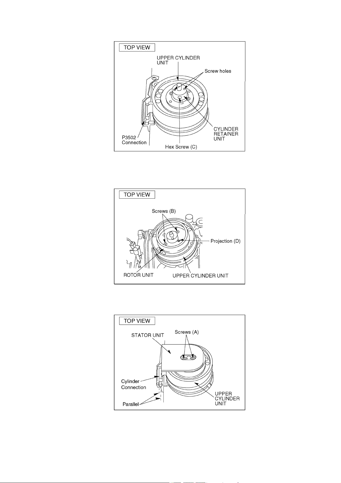
http://cxema.ru
3. Install the Cylinder Rotor Unit so that the inner hole of the Cylinder Rotor Unit fits to the small projection (D) on top of the
Upper Cylinder.
4. Tighten 2 screws (B).
Fig. S6
5. install the Cylinder Stator Unit.
6. Tighten 2 screws (A).
Fig. S7
7. Confirm the PG SHIFTER ADJUSTMENT with the alignment tape (PAL: VFJ8125H3F) and adjust it if necessary.
http://cxema.ru
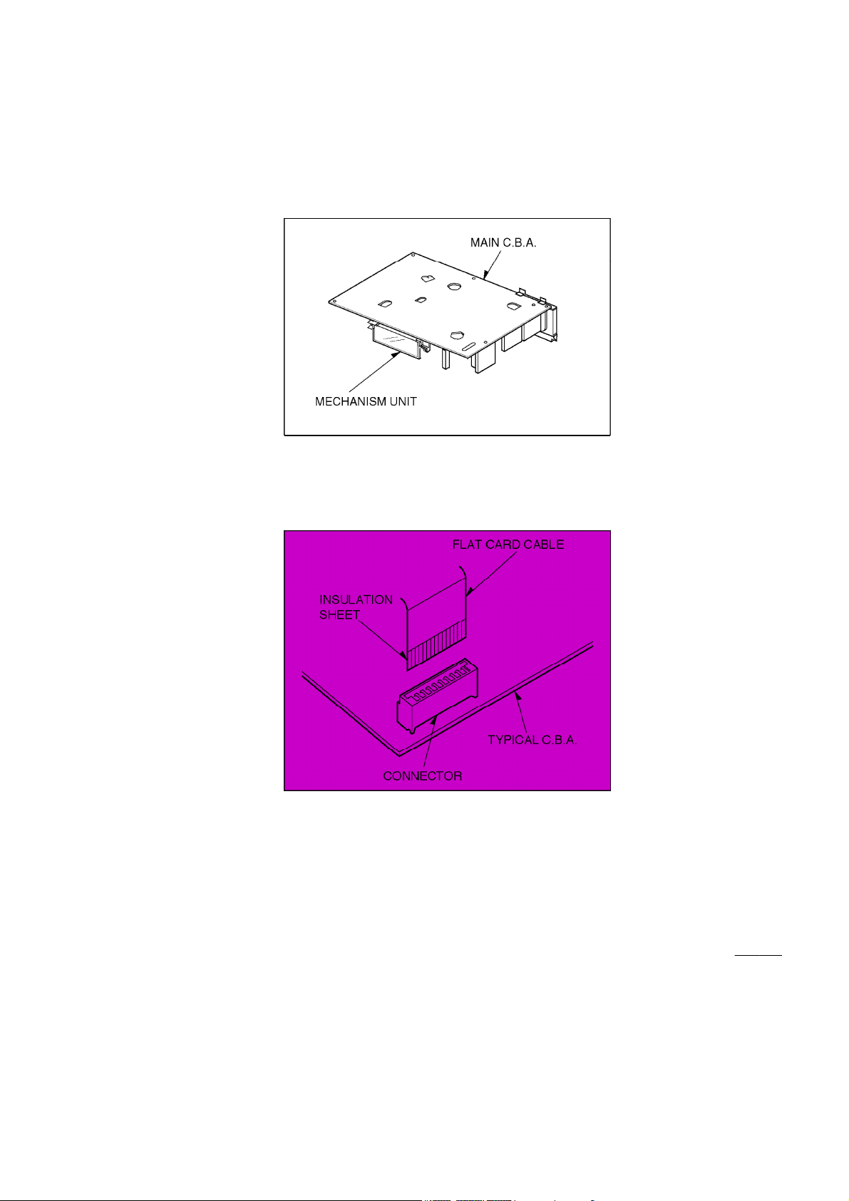
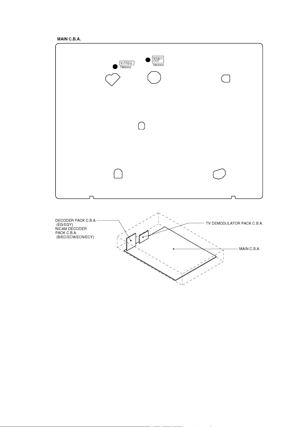
2.1.3. CHECKING OF MAIN C.B.A.
When servicing the MAIN C.B.A., take out the MAIN C.B.A. and mechanism from the frame and turn over.
Fig. S8
2.1.4. FLAT CARD CABLE INSTALLATION
When installing the Flat Card Cable on the connector, install the Flat Card Cable with the cable contacts
facing the connector contacts.
Fig. S9
2.2. REMOVAL OF CASSETTE TAPE
There are 2 ways to remove a cassette tape.
1. Service Information Display Operation
A. Press the FF and EJECT keys simultaneosly for 3 seconds and set the Service Mode 7.
B. Press STOP key in order to rotate the Loading Motor for unloading operation. (Pay an attention of tape slack)
2. Manual Operation
A. Disconnect the AC Mains Lead and remove the Top Panel.
B. Rotate the Main Cam Gear clockwise until the Loading Posts move to fully unloaded position as shown in
Fig. S10 .
(Tape is remaining)
Fig. S10
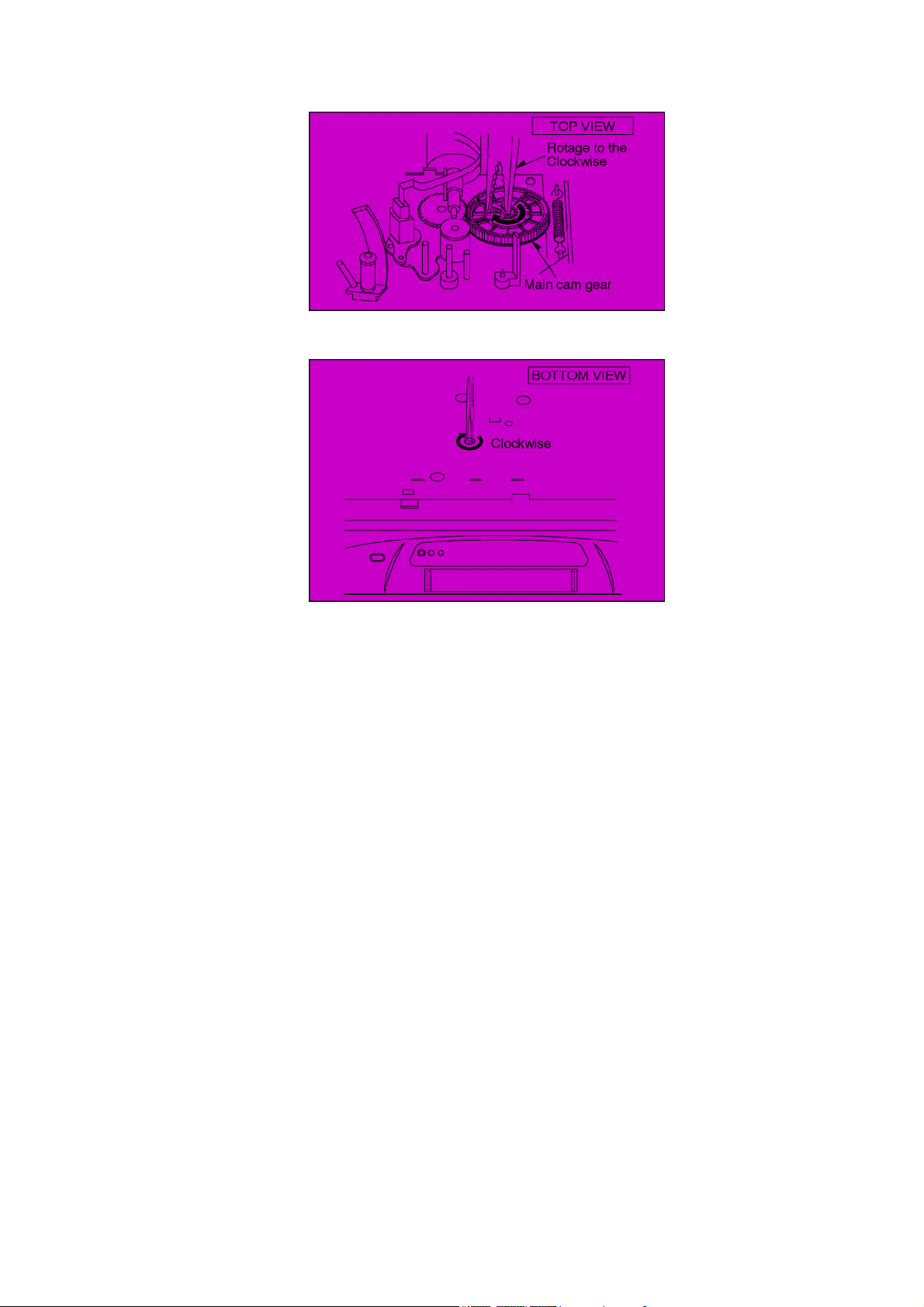
http://cxema.ru
C. Rotate the Capstan Motor clockwise from the bottom side to take up the tape.
Fig. S11
D. Rotate the Main Cam Gear clockwise until the cassette tape is ejected.
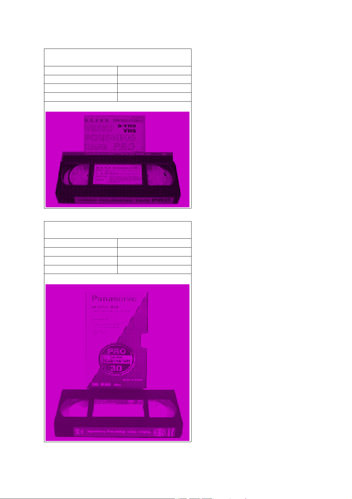
2.3. INTRODUCTION OF VIDEO HEAD CLEANING CASSETTE /
(POLISHING TYPE)
1. We are pleased to introduce Panasonic Video Head Cleaning Cassette, VFK0923FT [for service purposes] and
VFK0923FSE [ for end users] for all VHS/SVHS VCP and VCR.
2. These cleaning cassettes are exclusive removing the hard and sticky clogging on video heads.
3. These improve the efficiency of video head cleaning service and shortening cleaning time for end users.
http://cxema.ru
VFK0923FT
(For Service usage)
Type of Cassette Full VHS Cassette
Cleaning Time 10 Seconds/Time
Tape Length 20 m
Usability in a Path 180 Times
VFK0823FSE
(For end users)
Type of Cassette Full VHS Cassette
Cleaning Time 10 Seconds/Time
Tape Length 3.34 m
Usability in a Path 30 Times
http://cxema.ru
Note:
s
g
r
p
e
The tape material itself is the same in both types.
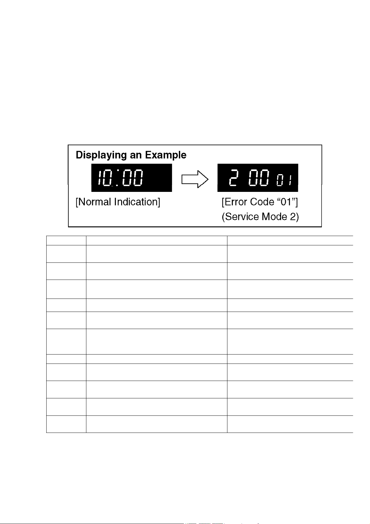
2.4. SELF-DIAGNOSIS RESULT DISPLAY
The "SELF-DIAGNOSIS RESULT DISPLAY & MEMORY function is built in this VTR.
It means that when the VCR detects undesirable condition, it can be displayed a “Error code (Two numbers
from the left)” with Service Mode 2.
Since the "Error code" is stored in the EEPROM, it can be displayed although after disconnected the AC leads.
It can be displayed with Service Mode 2.
(If a second error had been detected, only the most recent error is displayed. )
For more details, refer to the Service Manual for Z-Mechanism Chassis Order number VRD9612M129.
INDICATION CAUSE REMEDY/CHECK
01 After cylinder lock is detected, the cylinder does
Check the cylinder motor drive circuit.
not start rotating again even after tape unloading.
02 Cassette tape is not wound up during the tape
Check the capstan motor drive circuit.
unloading except EJECT mode.
03 Mechanism locks during mode transition except
EJECT mode.
04 Mechanism locks during tape unloading.
06 Mechanism locks after tape unloading in EJECT
mode.
07 During recording mode, recording signal is less
than the normal condition.
1. Check the loading motor drive circuit.
2. Check the mechanism phase alignment.
3. Check the mode switch.
1. Check the loading motor drive circuit.
2. Check the mechanism phase alignment.
1. Check the loading motor drive circuit.
2. Check the mechanism phase alignment for cassette holder un
Protection of the over-current flowing in transi
which produces the power supply for recordin
mode.
08 Recording circuit works except recording mode. Check the recording circuit.
16 Cylinder lock detection. Check the cylinder unit and the cylinder moto
drive circuit.
17 Supply reel mechanism lock detection Check the supply reel mechanism and the su
reel circuit.
18 Take-up reel mechanism lock detection Check the Take-up reel mechanism and the
Take-up reel circuit.
2* PG shifter automatic adjustment error. Check the servo/system control circuit and th
cylinder unit.
2.5. CAUTION FOR AC MAINS LEAD (NV-FJ621B)
Fig. T1 Self-Test indication Display
http://cxema.ru
3. ADJUSTMENT PROCEDURES
3.1. DISASSEMBLY METHOD
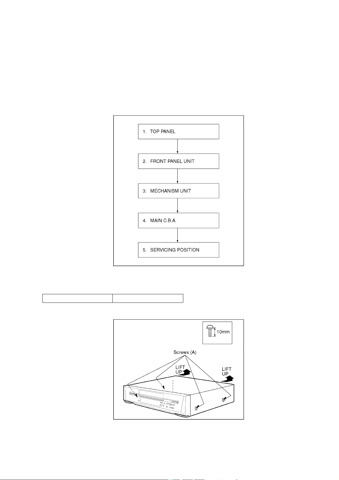
3.1.1. DISASSEMBLY FLOW CHART
This flow chart indicates disassembly steps of the cabinet parts and the circuit boards in order to find the
necessary items for servicing.
When reassembling, perform the steps in the reverse order.
Fig. D1
3.1.2. DETAIL OF DISASSEMBLY METHOD
1. REMOVAL OF THE TOP PANEL
Remove 4 Screws (A)
Fig.D2
2. REMOVAL OF THE FRONT PANEL UNIT
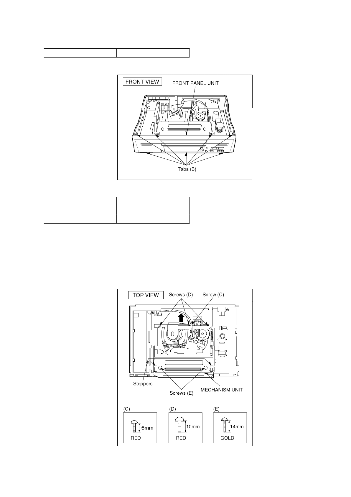
http://cxema.ru
Unlock 7 Tabs (B)
3. REMOVAL OF THE MECHANISM UNIT
Remove Screw (C)
Remove 3 Screws (D)
Remove 2 screw (E)
Fig. D3
Note:
1. Keep pressing 2 stoppers on Cassette Holder Plate and Press Cassette Holder Plate to the rear.
2. Remove the Mechanism Unit after bend the Cylinder Shield in the direction of the arrow.
Fig. D4
http://cxema.ru
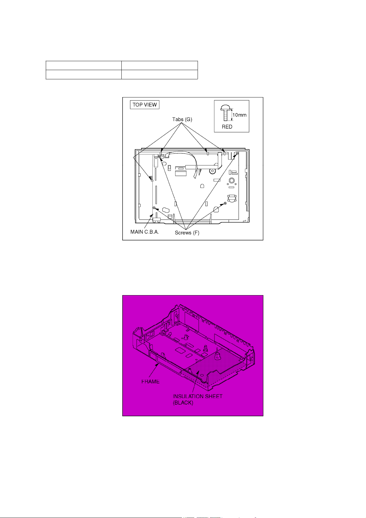
4. REMOVAL OF THE MAIN C.B.A.
Remove 4 screws (F)
Unlock 4 Tabs (G)
Fig. D5
NOTE:
Before mounting the MAIN C.B.A. onto the frame, be sure to confirm that the insulation sheet is mounted on
the frame as shown in Fig. D6.
Fig. D6
5. SERVICING POSITION
Fig. D7

http://cxema.ru
3.2. MECHANICAL ADJUSTMENT PROCEDURES
Refer to the Service Manual for Z-Mechanism Chassis. / (Order No. VRD9802005C2)
3.3. ELECTRICAL ADJUSTMENT PROCEDURES
3.3.1. TEST EQUIPMENT
The following equipments are required for Electrical Adjustments.
1. Dual-Trace Oscilloscope
- Voltage Range: 0.005-5V/div
- Frequency Range: DC-35MHz
- Probes: 10:1 / 1:1
2. Frequency Counter
- Frequency Range: 0-10MHz
- Probes: 1:1
3. Universal Counter
4. Digital Volt Meter (D.V.M.)
5. Video Sweep Generator
6. Sinewave Generator
7. Video Pattern Generator
8. Monitor TV
9. DC Power Supply
10. VHS Blank Tape
11. VHS Alignment Tape
3.3.2. VCR SETTING
When no indication in the procedure, set each selector as follows.
1. TAPE SPEED: SP
2. CHANNEL: AV1/AV2
(Set to signal input terminal number)
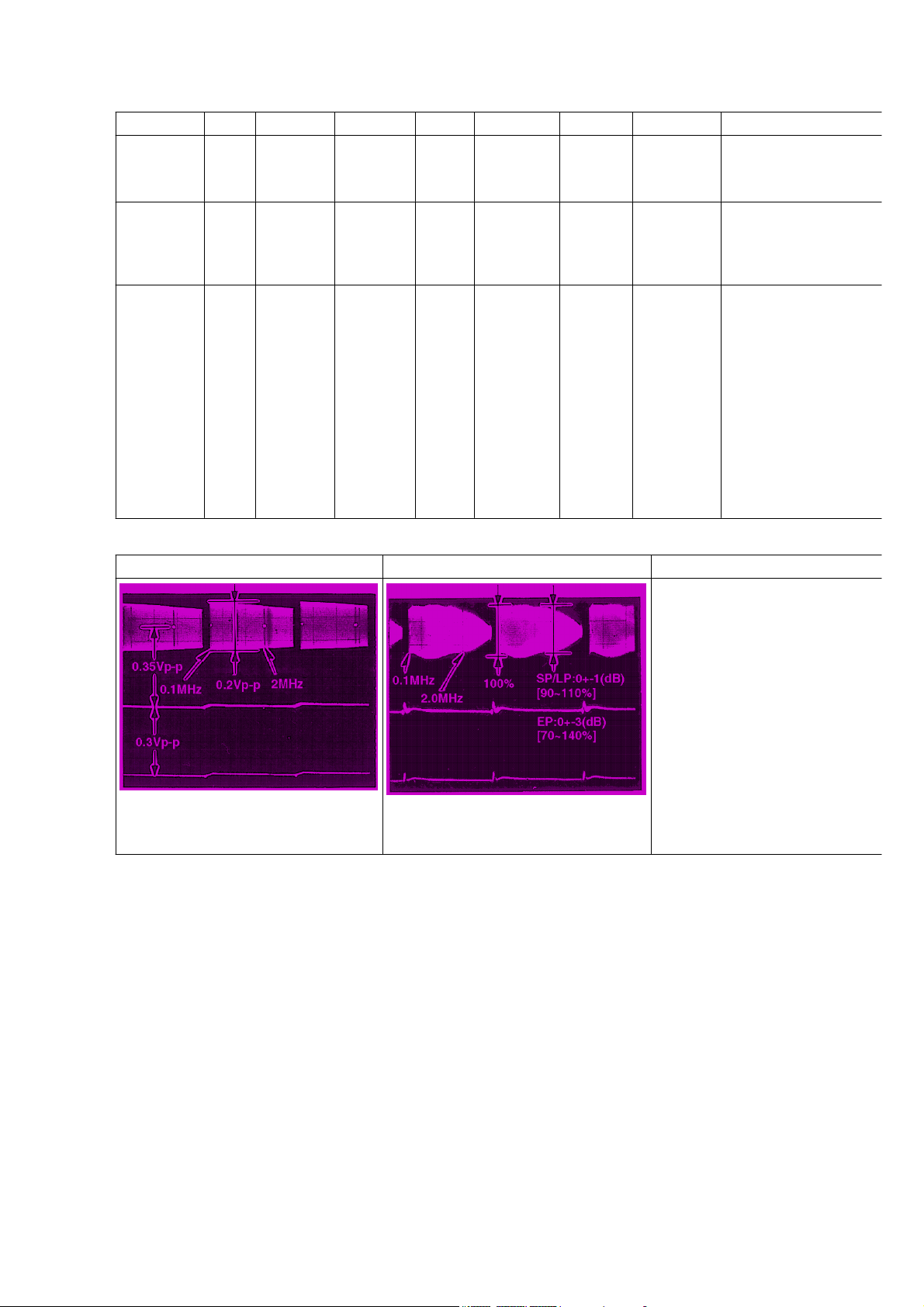
3.3.3. ADJUSTMENTS
- Parts No.: VFJ8125H3F(PAL)
http://cxema.ru
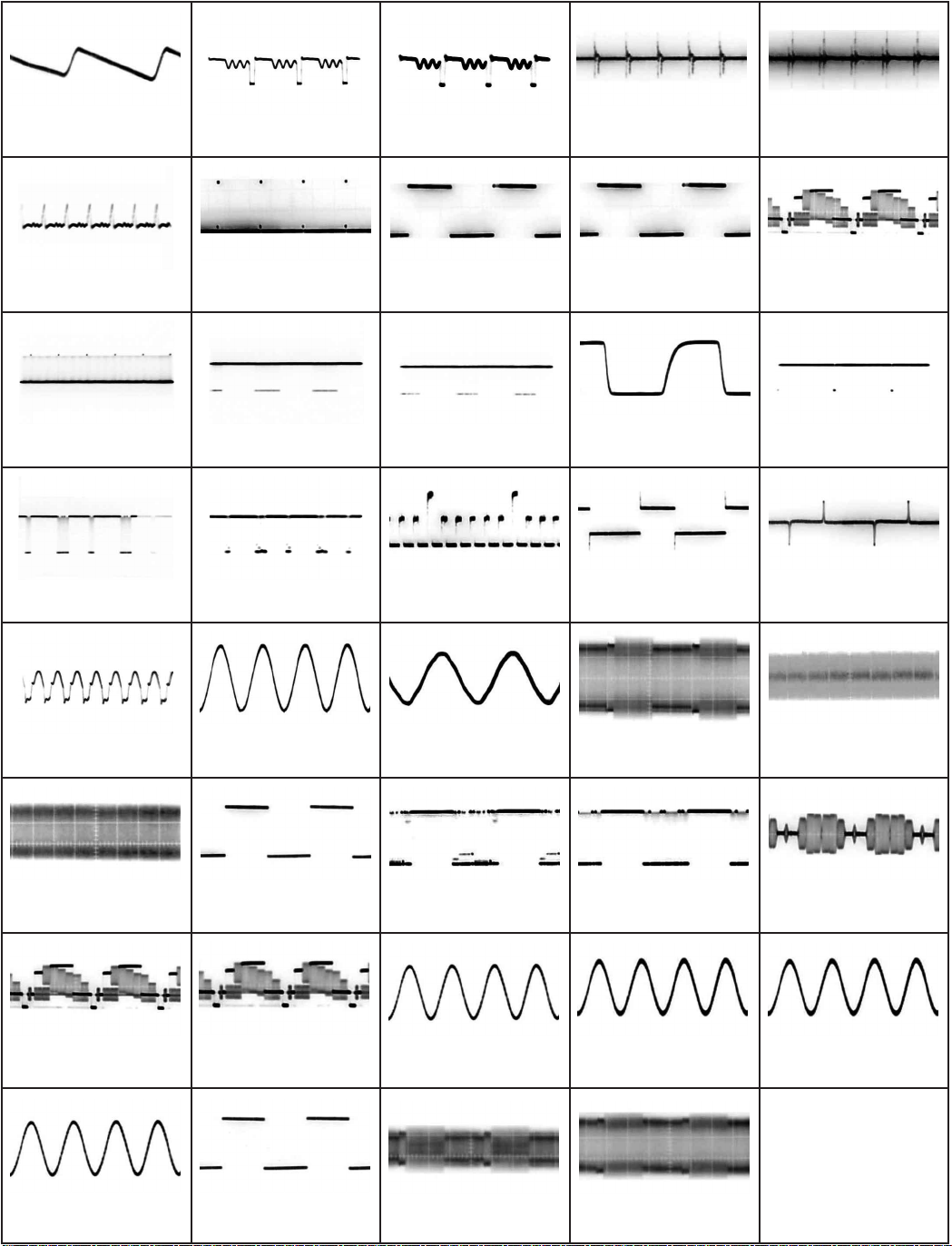
ITEM TP ADJ. MODE INPUT TAPE M. EQ. SPEC. REMARKS
P
N
w
w
PG
SHIFTER /
ADJUSTMENT
AI
FUNCTION
/
ADJUSTMENT
VIDEO /
FREQUENCY
/
RESPONSE
/
ADJUSTMENT
--- ---
--- ---
VIDEO
OUT
--- SP/LP/EP
Fig.E1 Fig.E2
PLAYBACK
PLAYBACK
/
(SELF-REC)
/
PLAYBACK
/
(SELF-REC)
---
PAL /
COLOUR
/ BAR
VIDEO
/
SWEEP
/ (See
Fig.E1)
ALIGNMENT
TAPE /
(PAL)
BLANK /
TAPE
BLANK
TAPE
--- --- Refer to procedure of
SHIFTER ADJUSTME
as shown in Fig.E3.
--- --- Refer to the procedure
AI FUNCTION
ADJUSTMENT as sho
in Fig.E4.
OSCILLO
/
SCOPE/
/ VIDEO
SWEEP
GENERATOR
SP: 0+-1
(dB)
(90~110%)
LP: 0+-1
(dB)
(90~110%)
EP: 0+-3
(dB)
(70~140%)
(See Fig.
E2)
Refer to the procedure
VIDEO FREQUENCY
RESPONSE
ADJUSTMENT as sho
in Fig. E5.
CONDITION: BURST SIGNAL OFF /
75 ohm TERMINATED
3.3.4. PG SHIFTER ADJUSTMENT / (AUTOMATIC)
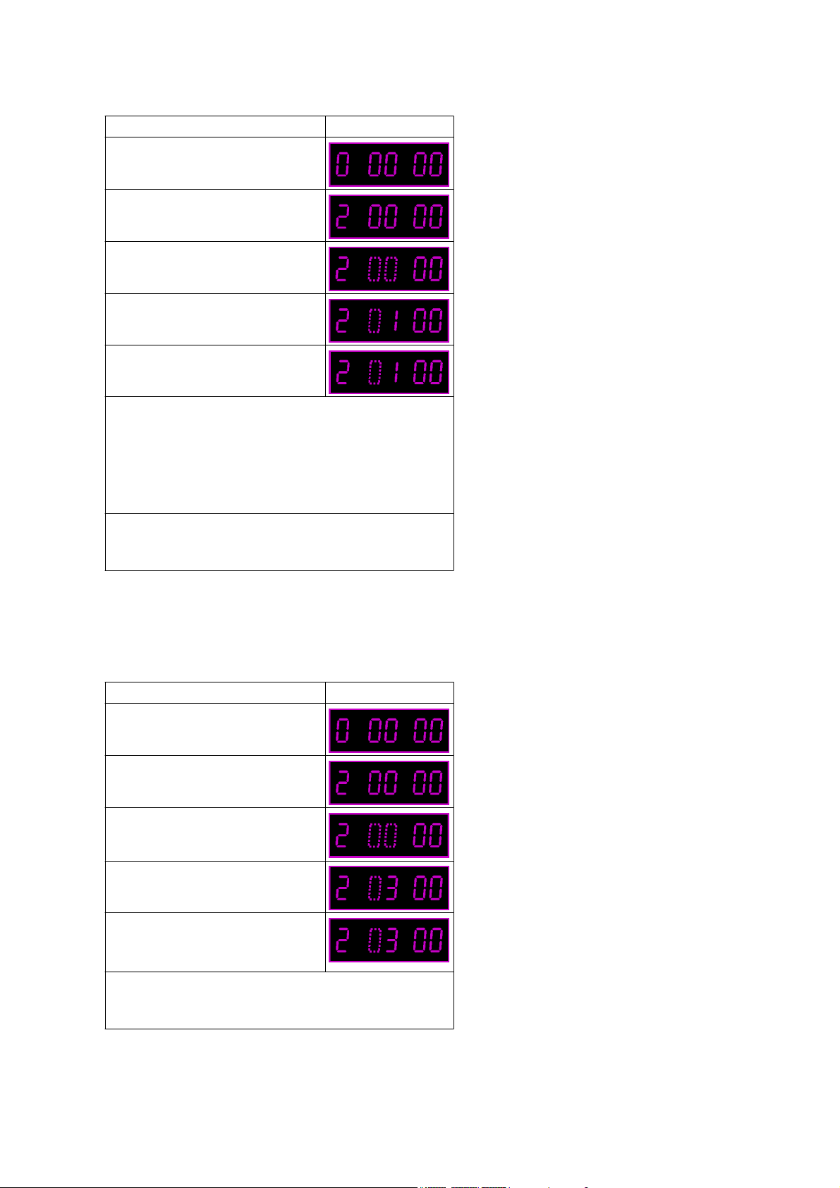
http://cxema.ru
PROCEDURES FIP DISPLAY
Press the FF and EJECT Keys
simultaneously for 3 seconds.
Press the FF and EJECT Keys
simultaneously twice.
Press the EJECT key for 3
seconds.
Press the CH UP key once.
Insert the Alignment cassette
tape. (PAL:VFJ8125H3F)
When the sequence of the automatical adjustment has
been terminated, the following action has been made.
*SUCCEED: The cassette tape is ejected.
*ERROR : The "F2"is displayed on the FIP.
(Check the Servo/Syscon circuit and Cylinder
unit.)
Release the Service mode by pressing the EJECT and
FF keys simultaneously in 6 times until the FIP
becomes normal indication.
Fig. E3
3.3.5. AI FUNCTION ADJUSTMENT (AUTOMATIC)
PROCEDURES FIP DISPLAY
Press the FF and EJECT Keys
simultaneously for 3 seconds.
Press the FF and EJECT Keys
simultaneously twice.
Press the EJECT key for 3
seconds.
Press the CH UP key in 3 times.
Insert the blank cassette tape.
(The adjustment is automatically
started.)
When the sequence of the automatical adjustment has
been terminated successfully, the VCR goes to STOP
mode.
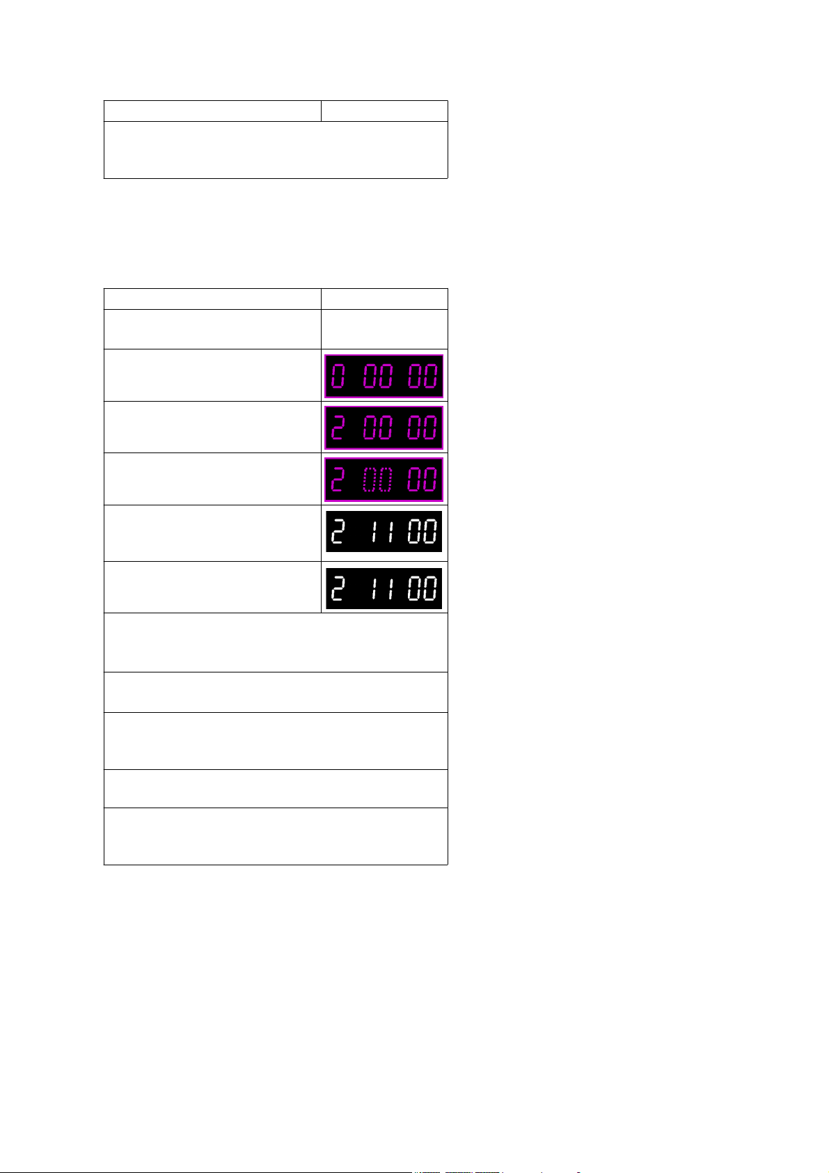
http://cxema.ru
PROCEDURES FIP DISPLAY
Release the Service mode by pressing the EJECT and
FF keys simultaneously in 6 times until the FIP
becomes normal indication.
Fig. E4
3.3.6. VIDEO FREQUENCY RESPONSE ADJUSTMENT
PROCEDURES FIP DISPLAY
Input the Video sweep signal.
(See Fig.E1)
Press the FF and EJECT Keys
simultaneously for 3 seconds.
Press the FF and EJECT Keys
simultaneously twice.
Press the EJECT key for 3
seconds.
Press the CH UP and/or CH
DOWN key until "11" is displayed
on FIP.
Insert the Self-recorded tape and
playback it. (SP/LP/EP mode)
Connect the Oscilloscope to:
*CH1....Video Out (TW3002).
*CH2....V.FREQ.(TW6002)
Press the "4" key on the remote controller.
(Confirm that TW6002 becomes high(5V)).
Adjust the Frequency response by pressing the
"2"(increase) and/or "8"(decrease) key on the Remote
Controller. (See Fig.E2)
Store the Adjusted value by pressing the "5" key on
the Remote Controller.
Release the Service mode by pressing the EJECT and
FF keys simultaneously in 6 times until the FIP
becomes normal indication.
Fig. E5
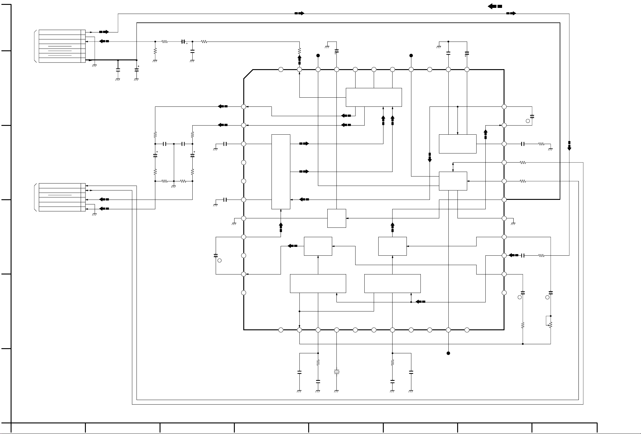
3.3.7. LOCATION OF TEST POINTS & CONTROLS
http://cxema.ru
3.3.8. CIRCUIT BOARD LAYOUT
T1101-3 STOP
9.0Vp-p (2msec. div.)
T1101-7 STOP
100Vp-p (5µsec. div.)
IC1101-1 STOP
470Vp-p (5µsec. div.)
IC1101-2 STOP
8.0Vp-p (10µsec. div.)
IC1101-4 STOP
0.5Vp-p (10µsec.div.)
IC1101-5 STOP
0.6Vp-p (10µsec.div.)
IC6001-68 REC
5.0Vp-p (10msec.div.)
IC6001-99 REC
5.0Vp-p (10msec.div.)
IC2501-1,2,16 REC
8.6Vp-p (5msec.div.)
IC6001-20 PAUSE
5.0Vp-p (10msec.div.)
IC6001-89 REC
5.0Vp-p (10msec.div.)
IC6001-100 REC
5.0Vp-p (10msec.div.)
IC3001-2 REC
1.2Vp-p (5msec.div.)
IC6001-21 REC
5.0Vp-p (10msec.div.)
IC6001-90,91 REC
5.0Vp-p (10msec.div.)
IC6001-107 REC
5.0Vp-p (10msec.div.)
IC3001-4 PLAY
5.0Vp-p (5msec.div.)
IC6001-24 REC
5.0Vp-p (10msec.div.)
IC6001-93,94 FF/REW
5.0Vp-p (1msec.div.)
IC6001-111,112 REC
6.0Vp-p (10msec.div.)
IC3001-14 REC
0.4Vp-p (5msec.div.)
IC6001-61 REC
2.4Vp-p (20µsec.div.)
IC6001-97,98 REC
5.0Vp-p (10msec.div.)
IC6001-114 PLAY
4.2Vp-p (10msec.div.)
IC3001-15 PLAY
0.5Vp-p (20µsec.div.)
IC3001-20 PLAY
150mVp-p (20µsec. div.)
IC3001-48,50 REC
1.0Vp-p (20µsec. div.)
IC4501-53,57
REC/PLAY
1.2Vp-p (5msec. div.)
IC3001-24 REC/PLAY
5.0Vp-p (10msec. div.)
IC3001-52 REC/PLAY
2.0Vp-p (20µsec. div.)
IC3501-1 REC/PLAY
5.0Vp-p (10msec. div.)
IC3001-37 REC/PLAY
5.0Vp-p (5msec. div.)
IC3001-78 REC/PLAY
1.2Vp-p (5msec. div.)
IC3501-30 PLAY
0.4Vp-p (5msec. div.)
IC3001-38 REC/PLAY
5.0Vp-p (5msec. div.)
IC4501-9,14 REC
1.2Vp-p (5msec. div.)
IC3501-31 REC
0.3Vp-p (5msec. div.)
IC3001-42,43 PLAY
0.4Vp-p (20µsec. div.)
IC4501-21 REC
1.2Vp-p (5msec. div.)
123
4
0.01.24.90
0.01.24.90
0.01.24.80
0.01.22.40
0.01.22.30
8910111213141
8910111213141
--4.90.01
2
--4.90.01
0
--4.90.01
--4.90.01
0
--4.90.01
4
0
0
0
8910111213141
4
4
8
ECBEC
B
B
4
1.60.00.90.04.90
4
1.60.00.90.04.90
4
1.60.00.90.04.90
4
1.60.00.90.04.90
4
1.60.00.90.04.90
ECBEC
B
1
0.00.04.90.00.04
1
0.01
0.00.04
1
0.00.04.90.00.04
1
0.00.04.90.00.04
1
0.00.04.90.00.04
I
Q
Q
I
I
I
Q
Q
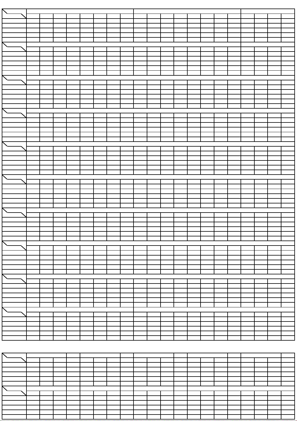
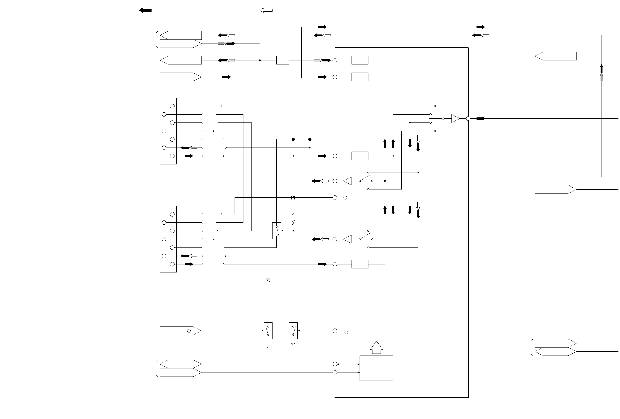
SYSTEM CONTROL & SERVO ICs DC VOLTAGE CHART (SP MODE)
I
I
I
I
I
Ref. No.
MODE1234
STOP 1.2 2.3 4.9 0.0
PLAY 1.2 2.3 4.2 0.0
REC 1.2 2.3 4.8 0.0
F.F 1.2 2.3 2.2 0.0
REW 1.2 2.3 2.4 0.0
Ref. No.
MODE1234567
STOP 16.8 16.8 16.8 4.94.9 1.2 1.10.02.71.50.04.14.13.70.0 16.8
PLAY 14.9 14.9 15.2 1.14.9 1.1 1.20.62.41.50.03.83.83.80.0 14.9
REC 15.1 15.1 15.4 1.04.9 1.1 1.20.62.41.50.03.83.83.80.0 15.1
F.F 14.4 14.4 14.6 1.04.9 1.1 1.20.62.41.50.03.83.83.80.0 14.7
REW 14.3 14.3 14.6 1.14.9 1.1 1.20.62.41.50.03.83.83.80.0 14.9
Ref. No.
MODE1234567
STOP 0.0 1.9 0.0 0.03.5 0.0 0.00.02.40.00.04.94.94.74.1 0.0 4 .9 0.00.00.0
PLAY 4.7 1.8 0.0 0.03.9 0.0 0.00.02.40.04.34.94.94.60.1 0.0 0 .0 0.00.00.0
REC 4.7 1.9 0.0 0.02.2 0.0 0.00.02.40.00.04.94.84.64.0 0.0 0 .0 0.04.90.0
F.F 4.9 1.8 0.0 0.03.5 0.0 0.00.02.40.00.04.94.84.84.1 0.0 4 .9 0.00.00.0
REW 4.9 1.8 0.0 0.03.4 0.0 0.00.02.40.00.04.94.94.64.1 0.0 4 .9 0.00.00.0
Ref. No.
MODE 21 22 23 2425262728293031323334353637383940
STOP 0.0 0.0 2.5 2.40.0 4.8 0.04.90.00.0
PLAY 2.4 0.0 4.9 2.4
REC 2.4 0.0 4.8 2.4
F.F 0.0 0.0 0.0 2.40.0 4.8 0.04.90.00.0
REW 0.0 0.0 0.0 2.4
Ref. No.
MODE 41 42 43 44
STOP 0.0 0.0 5.0 4.90.0 0.0 0.00.04.90.04.94.91.52.14.9 1.9 0 .0 2.44.90.0
PLAY 0.0 0.0 5.0 4.90.0 0.0 0.00.04.90.04.94.91.52.14.9 1.9 0 .0 2.44.90.0
REC 0.0 4.9 5.0 4.90.0 0.0 0.00.00.00.04.94.91.52.14.8 1.9 0 .0 2.44.90.0
F.F 0.0 0.0 5.0 4.94.9 0.0 0.00.04.90.04.94.91.52.14.9 1.9 0 .0 2.54.90.0
REW 0.0 0.0 5.0 4.94.9 0.0 0.00.04.90.04.94.91.52.14.9 1.9 0 .0 2.44.90.0
Ref. No.
MODE 61 62 63 6465666768697071727374757677787980
STOP 1.9 2.1 0.0 0.00.0 0.0 0.00.40.00.04.94.90.00.00.0 5.2 5 .2 0.00.02.7
PLAY 1.9 2.1 0.0 0.00.0 0.0 0.00.40.00.04.94.80.00.00.0 5.2 5 .2 0.02.42.4
REC 1.9 2.1 0.0 0.00.0 0.0 0.00.40.00.04.94.80.00.00.0 5.2 5 .2 0.02.42.4
F.F 1.9 2.1 0.0 0.00.0 0.0 0.00.41.60.04.94.80.00.00.0 5.2 5 .2 0.02.92.4
REW 1.9 2.1 0.0 0.00.0 0.0 0.00.41.60.04.94.80.00.00.0 5.2 5 .2 0.02.92.4
Ref. No.
MODE 81 82 83 84858687888990919293949596979899100
STOP 0.0 0.0 0.0 0.00.3 0.0 0.00.04.94.94.92.44.94.94.9 4.9 4 .8 4.84.14.1
PLAY 0.0 0.4 0.0 0.00.3 0.0 0.00.04.94.94.92.44.14.84.9 4.9 4 .8 4.84.24.1
REC 0.0 0.4 0.0 0.04.5 0.0 0.00.04.94.94.92.44.24.84.9 4.9 4 .8 4.84.14.0
F.F 0.0 4.8 0.0 0.00.3 0.0 0.00.04.94.94.92.42.32.34.9 4.9 4 .8 4.84.24.1
REW 0.0 4.8 4.9 0.00.3 0.0 0.00.04.94.94.92.42.22.34.9 4.9 4 .8 4.84.24.1
Ref. No.
MODE 101 102 103 104105 106 107108109110111112113114115 116
STOP 0.0 0.0 2.5 2.50.0 0.0 4.92.52.50.02.52.52.52.54.9 4.9
PLAY 0.0 0.0 2.5 2.5
REC 0.0 0.0 2.4 2.40.0 0.0 1.02.42.40.01.92.32.52.54.9 4.9
F.F 0.0 0.0 2.5 2.5
REW 0.0 0.0 2.5 2.5
Ref. No.
MODE1234567
STOP 0.0 0.0 0.0 4.84.8 0.0 0.40.04.92.50.02.50.02.52.5 1.5 1 .3 0.04.94.9
PLAY 0.0 0.0 0.0 4.84.8 0.0 0.40.04.93.00.03.10.03.53.1 1.5 1 .3 0.04.94.9
REC 0.0 0.0 0.0 4.8
F.F 0.0 0.0 0.0 4.8
REW 0.0 0.0 0.0 4.84.8 0.0 0.40.04.92.50.02.50.02.52.5 1.5 1 .3 0.04.94.9
Ref. No.
MODE1234567
STOP 0.0 0.0 0.0 0.04.8 4.8 4.94.9
PLAY 0.0 0.0 0.0 0.04.8 4.8 4.94.9
REC 0.0 0.0 0.0 0.04.8 4.8 4.94.9
F.F 0.0 0.0 0.0 0.04.8 4.8 4.94.9
REW 0.0 0.0 0.0 0.04.8 4.8 4.94.9
IC1501
C2501
C6001
C6001
.4 4.8 0.00.00.00.0
.0 4.8 0.04.90.00.0
.0 4.8 0.04.90.00.0
5464748495051525354555657585960
.0 0.0 1.12.52.50.02.52.52.52.54.9 4.9
.0 0.0 1.02.52.50.02.52.52.52.55.0 5.0
.0 0.0 1.12.52.50.02.52.52.52.55.0 5.0
.8 0.0 0.40.04.92.40.02.50.02.52.5 1.5 1 .3 0.04.94.9
.8 0.0 0.40.04.92.50.02.50.02.52.5 1.5 1 .3 0.04.94.9
IC7702
C6001
C6001
C6001
C6001
C7701
C1502
.0
.0
.0
.0
.0
516
51617181920
.5 3.0 0 .0 0.00.04.9
.5 3.0 4 .9 0.00.04.9
.5 3.0 0 .0 4.94.90.0
.5 3.0 0 .0 0.00.04.9
.5 3.0 0 .0 0.00.04.9
51617181920
SYSTEM CONTROL & SERVO TRs DC VOLTAGE CHART (SP MODE)
Ref. No.
MODE
STOP 4.7 0.0
PLAY 4.7 0.0
REC 4.6 0.0
F.F 4.7 0.0
REW 4.9 0.0
Ref. No.
MODE E C B E C B
STOP 0.0 4.2 0.0
PLAY 0.0 4.2 0.0
REC 0.0 4.2 0.0
F.F 0.0 4.2 0.0
REW 0.0 4.2 0.0
Q1501 Q1502
+- +-
Q7704 Q7705
.9 0.0
.9 0.0
.8 0.0
.9 0.0
.9 0.0
.2 4.9 1.9
.3 4.9 1.9
.2 4.9 1.9
.2 4.9 1.9
.2 4.9 1.9
7701
R6001
2.30.0
7702
.0 0.0 0.00.6
.0 0.0 0.00.6
.0 0.0 0.00.5
.0 0.0 0.00.5
.0 0.0 0.00.5
R6006
.9
.8
.8
.8
.8
Q7703
EC
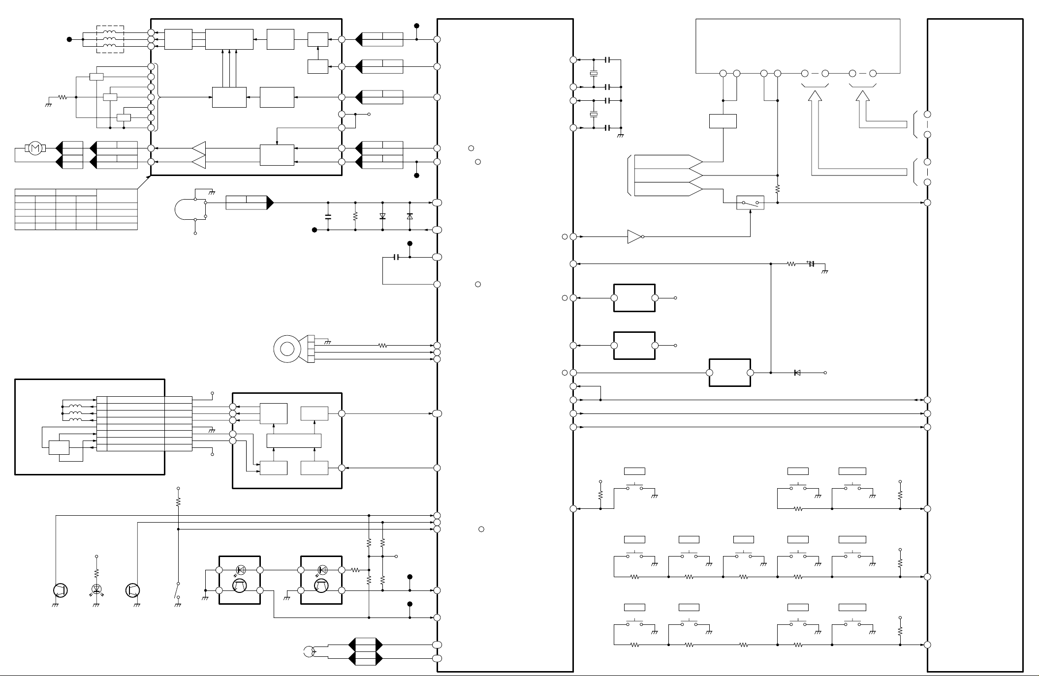
AUDIO
OUT (R)
AUDIO
OUT (L)
JK4902
(AV2)
DECODER/EXT
TO
TUNER
FROM
DECODER
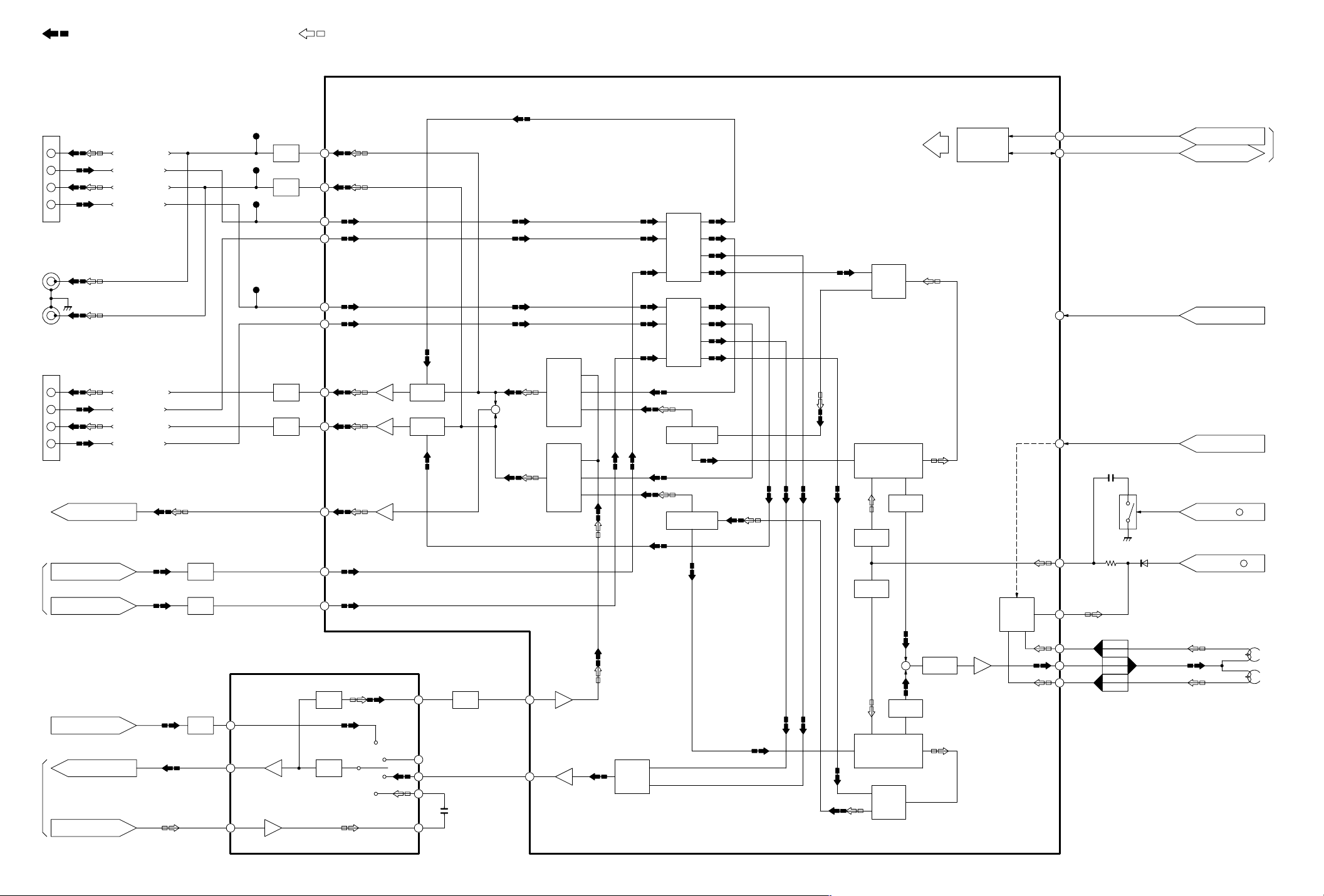
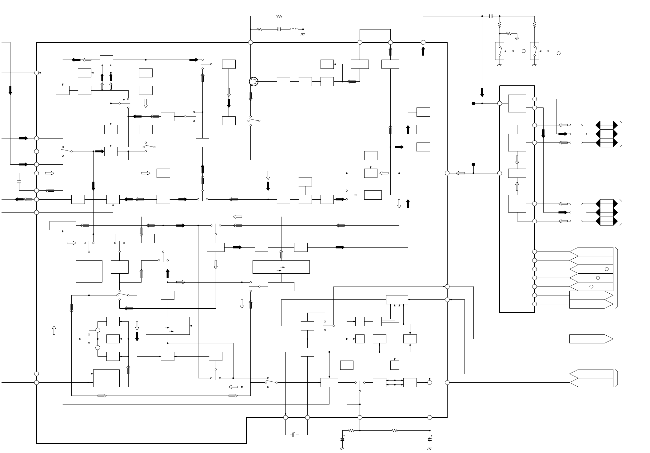
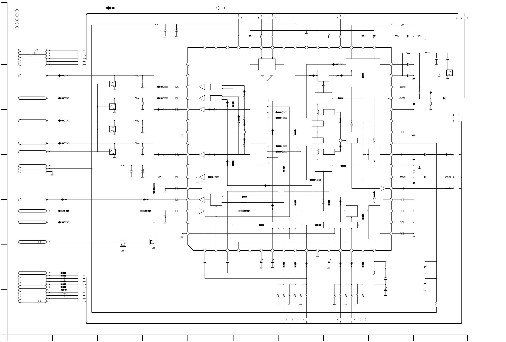
MAIN SIGNAL PATH IN REC MODE
JK4903
(AV1)
TV
1
2
3
6
JK4901
1
2
3
6
RFC AUDIO OUT
TUNER AUDIO (R)
TUNER AUDIO (L)
AUDIO OUT (R)
AUDIO IN (R)
AUDIO OUT (L)
AUDIO IN (L)
AUDIO OUT (R)
AUDIO IN (R)
AUDIO OUT (L)
AUDIO IN (L)
QR7604
MUTE
QR7603
MUTE
TW4907
TW4903
TW4902
TW4901
QR4502
MUTE
QR4501
MUTE
QR4503
MUTE
QR4504
MUTE
MAIN SIGNAL PATH IN PLAYBACK MODE
IC4501
53
57
9
10
14
15
51
52
59
8
13
SWITCH
RCH
SWITCH
LCH
+
OUTPUT
SELECT
SWITCH
RCH
OUTPUT
SELECT
SWITCH
LCH
INPUT
SELECT
SWITCH
RCH
INPUT
SELECT
SWITCH
LCH
PNR RCH
PNR LCH
AGC
&
SWITCH
FM MODULATOR/
DEMODULATOR
LPF
BPF
BPF
IIC BUS
INTERFACE
PREAMP
&
SWITCH
VCO
F0
42
43
45
27
30
29
SYS IIC CLOCK
SYS IIC DATA
FSC
AUDIO H.SW
PB 60Hz
H
D.FM REC
L
TO/FROM
SYSTEM
CONTROL
FROM
LUMINANCE &
CHROMINANCE
FROM
SYSTEM
CONTROL
FROM
SYSTEM
CONTROL
FROM
SYSTEM
CONTROL
FROM
DECODER/
TV DEMODU
TO/FROM
AC HEAD
TUNER AUDIO (N)
A.HEAD (W)
A.HEAD (R)
QR7601
MUTE
IC3001
75
2
4
SW
GAIN
ALC
QR4004
78
71
73 61
8
7
MUTE
24
AGC
+
62
FM MODULATOR/
DEMODULATOR
NORMAL
SELECT
SWITCH
AGC
&
SWITCH
LPF
21
22
P3502
8
P3502
9
P3502
10
L
Hi-Fi
AUDIO
HEAD
R
PIN 15
LOADING
MOTOR
INPUT
PIN 16
H
L
L
TL0201
P1501H2P2501 P0201
1
P1501
2
OUTPUT
PIN 21
PIN 19
L
H
H
L
H
L
LH
OPEN
L
H
L
OPEN
CAPSTAN
MOTOR
L0201
H3
H1
9
P2501 P0201
8
MODE
FORWARD
REWIND
BRAKE
STOP
(CAPSTAN MOTOR DRIVE)
IC0201
24
MOTOR
22
DRIVE
25
1
2
3
4
5
6
9
19
21
R0206
CAPSTAN
FG HEAD
CAP FG5V
DIFFERENTIAL
AMPRIFIER
POSITION
SIGNAL
PROCESS
P0201 P2501
4
TORQUE
CONTROL
TORQUE
DIRECTION
CONTROL
LOGIC
TL
AMP
EC
AMP
TW2015
12
10
7
26
18
15
16
P0201 P2501
1
P2501P0201
2
P2501P0201
3
REG
14V
P2501P0201
12
P2501P0201
11
TL2503
TL2502
TW2002
IC6001
(SYSTEM CONTROL/SERVO IC)
CURRENT
1
LIMIT
CAPSTAN
ERROR
79
TORQUE
CAPSTAN
83
REVERSE/
FORWARD
67
66
104
103
LOADING
UNLOADING
CAPSTAN
FG IN
CAPSTAN
FG OUT
H
H
20MHz IN
20MHz OUT
32KHz IN
32KHz OUT
FIP
L
DP7501
TIMER DISPLAY
31
X6002
32
34
X6001
35
HEATER(+)
FROM
POWER
48
HEATER(-)
UNREG -29V
QR1001
Q1001
BUFFER
F+F+
21
Q1006
F-F-
5
2333394544
IC7501
SEG1
36
|
SEG18
18
GRID1
11
|
GRID7
17
VEE
19
CYLINDER STATOR UNIT
MAIN COIL 2
MAIN COIL 1
MAIN COIL 3
HALL
IC
REG
5V
Q1501
TAKE UP
PHOTO
SENSOR
D1501
SENSOR
LED
P2901
6,7
1
9
3
5
8
4
2
VM
M2
M1
M3
GND
HEHE+
VH+
Q1502
SUPPLY
PHOTO
SENSOR
P2501-3,4
P2501-9
P2501-1
P2501-7
P2501-5
P2501-2
P2501-6
P2501-8
N.SW
5V
S7507
SAFETY
TAB SW
S1501
MODE
SW
REG
14V
REG
5V
IC1501
(T-REEL SENSOR)
12
4
(CYLINDER MOTOR DRIVE)
IC2501
2
1
16
7
6
SCHMIT
3
MOTOR
DRIVE
1
2
3
4
PG/FG
DIFFERENTIAL
AMPLIFIER
TORQUE
CONTROL
IC1502
(S-REEL SENSOR)
12
43
CTL
HEAD
114
CTL OUT
69
EX.FF/REW
33
BACK UP 5V
L
76
P.FAIL
L
IC7504
12
RESET
N.SW
5V
C7507
IC7502
45
POSITION SW2
44
POSITION SW3
46
POSITION SW1
107
4
9
REG
5V
TL6013
TL6012
P4003
5
P4003
6
CYL PFG
CYLINDER
ERROR
80
TORQUE
14
TAKE-UP PHOTO
13
SUPPLY PHOTO
65
SAFETY TAB
94
S-REEL PULSE
93
T-REEL PULSE
111
CTL HEAD(-)
112
CTL HEAD(+)
L
IR
RESET
L
S.DATA IN
S.DATA OUT
S.CLOCK
FIP CS
POWER SW
77
52
90
91
89
92
43
IR
13
RECEIVER
N.SW
5V
POWER
S7506
FF
S7514 S7513
REW
N.SW
5V
IC7503
RESET
12
T.REC
PLAY
S7511S7512
STOP
S7515
EJECT
S7505
REC
S7501
PAUSE
N.SW
5V
EXT LINK
S7508
CH DOWN
S7502
CH UP
S7504S7503
N.SW
5V
N.SW
5V
N.SW
5V
1
SERIAL DATA
2
SERIAL CLOCK
CS
3
5
A2
A5
6
7
A4
MAIN SIGNAL PATH IN REC MODE
MAIN SIGNAL PATH IN PLAYBACK MODE
TO/FROM
SYSTEM
CONTROL
TO TUNER
FROM TV
DEMODULATOR
Y/C VIDEO OUT
VIDEO OUT
RFC VIDEO OUT
TUNER VIDEO
JK4903
(AV1)
TV
8
7
11
15
16
19
20
JK4902
(AV2)
DECODER/EXT
8
7
11
15
16
19
20
PB +12V
BLUE
GREEN
RED
BLANKING
VIDEO OUT
VIDEO IN
PB +12V
BLUE
GREEN
RED
BLANKING
VIDEO OUT
VIDEO IN
Q4904
AMP
Q4903
PS
12V
IC4901
TO
SYSTEM
20
7
TW3002TW3003
36
34
33 PB
26
28
CLAMP
CLAMP
18
CLAMP
H
CLAMP
CONTROL
FROM
SYSTEM
CONTROL
C SYNC
ART V/H/N
FROM
SYSTEM
CONTROL
TO/FROM
SYSTEM
CONTROL
AV1 PB
OSD IIC DATA
OSD IIC CLOCK
Q4901
H
PS
12V
QR4903
RGB
16
OFF
H
TO/FROM
SYSTEM
CONTROL
2
3
IIC BUS
INTERFACE
SYS IIC CLOCK
SYS IIC DATA
IC3001
56
48
46
50
43
42
52
54
1H
DELAY
COLOUR
KILLER SW
HSS
LPF
AMP
VV
BPF
(FAMI)3.58M
(PAL-PB)2.2M
(NTSC-PB)
1.79M
67
EE/
FAMI
VV
EE
EE
VV
MAIN
LPF
VV/FAMI
EE VV
630KHz
BPF
NLE
NLDE
DTE
EE
FAMI
VV
FAMI
CACC
BM-B
(PB)2.2/1.79M 4.43/3.58M
(FAMI)2.2M 4.43M
NTSC
VV
ALTERNATION
SUB
LPF
MAIN
EMPH
W/D
CLIP
REC-C
ADJ
FM
DEM
DEV
ADJ
ENV
DET
DOUB
LIM
FM
MOD
YNR
NC1
PICT
DDC
NOR
CLP1
DET
Y/C
AGC
C
ART
SYNC
FAMI
EE
BPF
3.58M/
4.43M
EE
FAMI
VV
FAMI
FAMI/VV
VV
EE
NC2
Y/C
VV/
FAMI
C
Y
Y/C
MIX
SUB
CLAMP
BURST
UP/DOWN
LPF
Y
EE
20
PEAKING
AGC
DET
RF
AGC
VV
EE
L-TRAP
&HPF
19
H-TRAP
PHASE
ROTATION
14
TW3030
C
Y/C
MIX
REC-Y
ADJ
Y
LPF
TW3001
Y
C
15
27
24
QR3502
IC3501
31
30
LP
AMP &
H.AMP
SW
PREAMP
& H.SW
H.AMP
SW
PREAMP
& H.SW
QR3501
H
10
23
25
32
27
34
PAL
EP
H
3
HEAD SW
H.AMP SW
CURR.EMPH
H
D.REC
H
LP
P3502
3
P3502
2
P3502
1
P3502
6
P3502
5
P3502
4
H
TO/FROM
CYLINDER
VIDEO
HEAD
TO/FROM
CYLINDER
VIDEO
HEAD
TO/FROM
SYSTEM
CONTROL
7
9
4
6
1
2
LP L
LP COM
LP R
SP L
SP COM
SP R
TRACKING ENV.
ENV. SELECT
2HDL
1HDL
+
0HDL
+
0HDL
38
37
FAMI MODE:When setting the NTSC CONVERTER to ON on the OSD Screen Display,
the signals from NTSC Signal Source (ex.NTSC GAME Machine)connected
to the VCR can be appeared on the PAL TV.However when recording,
IIC BUS
TRANSCEIVER
it is not recorded correctly.
BM-A
(REC)4.43/3.58M
(PB)630K 2.2/1.79M
(FAMI)3.58M 2.2M
ACC
ACC
DET
EE
EE
VV
VV LP
FAMI/
VV SP
31
X3001
X2
VXO
30
2fsc
fsc
APC
CK DET
VCO
1/4
1/2
1/4
VV
25
SUB
BM
EE
AFC
1/40
F.DET
SIDE
LOCK
FH
PB Q
+
12
ADJ
23
FSC
ROTARY SW
F.ADJ.
TO
SYSTEM
CONTROL/
Hi-Fi AUDIO
FROM
SYSTEM
CONTROL
R0206
(FG HEAD)
D
P0201
CURR LIMIT
CAP ET
CAP ED/S
CAP FG1
GND (FG)
REG 5V
GND (MOTOR)
LOAD MOTOR (-)
C
TO SYSTEM CONTROL & SERVO
LOAD MOTOR (+)
PS 14V
UNLOADING
LOADING
SECTION P2501(F-21)
B
1234
R0213
R0212
Q0203
1
2
3
4
5
6
7
8
9
10
H
11
H
12
C0201
R0207
HOLE
HOLE
SENSOR
SENSOR
H3
H3
R0208
HOLE
SENSOR
H1
R0209
HOLE
SENSOR
H2
43
12
34
21
34
21
R0201 R0211
IC0201
(CAPSTAN MOTOR DRIVE)
RCC SET
H3-
1
+
2
H3+
H1-
3
+
4
H1+
H2-
10
11
12
13
14
5
6
7
8
9
H2+
ED/S
GND
VH+
EC
ECR
TL
PCV
PC1
+
TORQUE
DIRECTION
EC AMP
VCC
HALL
POWER
POSITION SIGNAL
PROCESS
TL
AMP
DIFFERENTAL AMP
AMP
VM1
A3
A1
A2
TSD
DRIVER
DRIVER
CONTROL
LOGIC
VCC
NC
VM1
A3
A1
ATC
A2
OUT2
RNF
OUT1
VM2
RIN
FIN
28
27
26
25
24
23
22
21
20
19
18
17
16
15
D0203
R0204
R0210
TL0204 TL0202 TL0203
C0208
C0209
TL0205
C0210
Q0202
Q0201
L0201
1
2
34
CAPSTAN MOTOR
MAIN COIL
TL0201
6
5
A
C0206
1
2345
C0207
67
CYLINDER SERVO SPEED LOOP
A
MAIN COIL 2
MAIN COIL 3
HALL IC
MAIN COIL 1
P2901
1
2
3
4
5
6
7
8
9
M2
VH+
M3
HE+
GND (CYL)
VM
VM
HEM1
TO SYSTEM CONTROL
& SERVO SECTION
P2502(B-21)
NOTE:DO NOT USE ANY PART NUMBER SHOWN ON THIS SCHEMATIC DIAGRAM FOR
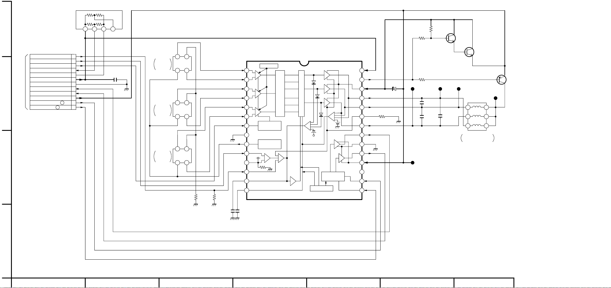
ORDERING.WHEN YOU ORDER A PART,PLEASE REFER TO PARTS LIST.
123
AUDIO SIGNAL PATH
E
D
F
PK7301
SIF
GND
TUNER AUDIO (N)
TO POWER SUPPLY/RF
TO POWER SUPPLY/RF
TUNER 5V
SECTION PK7301
(C-10)
PK7302
SYS IIC CLOCK
SYS IIC DATA
TUNER AUDIO (R)
GND
TUNER AUDIO (L)
SECTION PK7302
(B-10)
1.6
1
2
0
3
4
5
6
5.0
7
C7316
0.1
5.0
1
5.0
2
3
0
4
5
0
6
C7317
6V100
R7314
3300
R7307
6800
C7313
16V10
R7318
0
R7315
0
C7327
1500P
R7320
3300
C7318
16V10
C7326
1500P
C7328
1500P
R7319
3300
R7316
6800
R7308
6800
C7312
16V10
R7317
0
C7310
0.01
C7309
0.01
IC7301
TDA7873H
2.4
1
2.4
2
2.4
3
0
4
0
5
2.4
6
7
R7309
220
0
2.4
44 43 42 41 40 39 38 37 36 35 34
STEREO
DECODER
STEREO
ADJUST
TL7302
0
C7319
16V47
2.4 2.4 2.4 2.4
AF SWITCH
POWER
SUPPLY
TL7301
00
C7320
4700P
2.5 2.5
DIGITAL
IDENTIFICATION
PILOT
NARROW-BAND PLL
IIC BUS
TRANSCEVER
C7321
50V0.47
2.4
33
C7322
50V0.47
C7323
0.1
R7312
100
R7313
100
N
R7311
7500
2.4
32
2.9
31
5.0
30
5.0
29
5.0
28
27
C
B
A
C7308
50V0.47
2.4
8
0
2.4
9
10
0
11
12 13 14 15 16 17 18 19 20 21 22
00
N
AF
AMPLIFIER
1
FM DEMODULATOR
NARROW-BAND
PLL SC1
2.9 2.6
R7306
C7307
680P
5600
C7306
0.012
00
X7301
VSX1086
AF
AMPLIFIER
2
FM DEMODULATOR
NARROW-BAND
PLL SC2
2.8
00
R7305
5600
C7305
0.012
C7304
680P
2.3
TL7303
0
1.4
26
C7301
2.4
0.01
25
1.5
24
0
23
N
C7303
50V0.47
R7304
4700
R7301
0
N
C7302
50V0.47
VR7301
10KB
DO NOT USE ANY PART NUMBER SHOWN ON THIS SCHEMATIC DIAGRAM FOR
NOTE:THE MEASUREMENT MODE OF THE DC VOLTAGE ON THIS DIAGRAM IS STOP MODE.
NOTE:
ORDERING.
WHEN YOU ORDER A PART,PLEASE REFER TO PARTS LIST.
1234567
8
:TO POWER SUPPLY/RF SECTION
R
:TO SYSTEM CONTROL & SERVO SECTION
S
V
:TO LUMINANCE & CHROMINANCE/AUDIO SECTION
:TO INPUT/OUTPUT SECTION
I
:TO TIMER SECTION
T
G
D.FM REC
S
PB 60Hz
S
MUTE
S
SYS IIC CLOCK
S
SYS IIC DATA
S
FSC
V
AUDIO OUT2 (R)
I
H
H
H
A6
A5
A4
A3
A2
A1
F
AUDIO OUT2 (L)
I
I
AUDIO OUT1 (R)
E
AUDIO OUT1 (L)
I
P.FAIL MUTE
T
PS 12V
R
PS 5V
R
GND
R
D
AUDIO IN (N)
V
AUDIO OUT (N)
V
RFC AUDIO OUT
C
R
AUDIO MUTE
S
H
AUDIO MAIN SIGNAL PATH IN REC MODE
L4503
1.2u
R4529
220
-0.4
-0.4
-0.4
-0.4
0
QR4503
UN2216
(MUTE)
0
QR4504
UN2216
(MUTE)
0
QR4502
UN2216
(MUTE)
0
QR4501
UN2216
(MUTE)
L4501
0
QR4505
UN2113
(BUFFER)
0
R4531
220
R4536
220
R4535
220
C4537
0.01
-0.4
R4530
100K
R4532
100K
R4533
100K
R4534
100K
C4538
16V47
R4528
390
0
QR4506
UN2216
(MUTE)
C4524
0.01
R4527
4700
C4525
6V100
0.2
0.5
C4529
16V10
5.8
C4530
16V10
5.8
C4531
16V10
5.8
C4532
16V10
5.8
12.3
C4533
16V10
6.0
C4534
10V22
0.7
C4535
16V10
2.4
C4536
0.1
2.4
IC4501
AN3656NFBP
48 47 46 45 44 43 42 41 40 39 38 37 36 35 34 33
49
50
51
52
53
0
54
GND
55
0
56
57
VCC2
58
59
60
61
62
63
64
SWITCH
RCH
SWITCH
LCH
DET
NORMAL
OUTPUT
SWITCH
123456789
2.3
C4540
0.1
B
TUNER AUDIO (R)
R
AUDIO IN1 (R)
I
AUDIO IN2 (R)
I
TUNER AUDIO (L)
R
AUDIO IN1 (L)
I
AUDIO IN2 (L)
I
AUDIO HEAD COM
V
AUDIO HEAD R
V
AUDIO HEAD L
V
A.HEAD SW
S
ABS NORMAL
S
H
B10
B11
B1
B2
B3
B4
B5
B6
B7
B8
B9
AUDIO MAIN SIGNAL PATH IN PLAYBACK MODE
A1 A2 A3 A4
R45370C4528
2.0 3.2 4.2 4.3 4.9
VCO-
FO
+
0
2.3
00
C4541
0.1
16V10
OUTPUT
SELECT
SWITCH
RCH
OUTPUT
SELECT
SWITCH
LCH
R45241KR4525
1K
IIC BUS
INTERFACE
INPUT SWITCH RCH INPUT SWITCH LCH
VREF
2.4 2.0
C4501
16V10
000
C4502
16V10
R4510 10K
R4517 22K
R4511 5600
R4522
R4538
30K
1K
0
VCC
10 11 12 13 14 15 16
R4509 68K
R4503 68K
R4504 5600
1.7
GND(R)
REC AGC
AGC &
SWITCH
FM
MODULATOR/
DEMODULATOR
LPF
BPF
BPF
LPF
FM
MODULATOR/
DEMODULATOR
GND
(L)
2.0
0
MUTE
CONTROL
ADJ.
+
000
C4503
16V10
R4513 10K
R4518 22K
R4514 5600
2.4
AGC
AGC &
SWITCH
R4512 68K
0.3
(0.7)
PNR RCH
R4501 68K
R4502 5600
C4521
16V10
2.54.72.52.5
PREAMP
&
SWITCH
PNR
LCH
2.4
C4520
16V22
REC AGC
DET
ENV.DET
OUT
R4515
4700
REC
DC2
VCC
GND
32
31
30
29
28
27
26
25
24
23
22
21
20
19
18
17
R4516
510
C4504
0.047
C4505
10V33
2.5
2.4
(1.0)
1.7
(4.1)
1.8
(4.3)
0.1
(4.1)
2.4
(0)
0
(2.0)
4.9
0.7
(2.0)
0.7
(2.0)
0
(1.8)
0
(1.9)
2.5
2.5
0.3
(0.7)
R4521
510
R4523
4700
C4516
0.1
C4509
0.033
C4508
0.015
C4507
16V22
C4506
16V10
C4522
0.047
R4520
120K
C4519
0.015
C4518
0.22
C4512
150P
C4511
150P
R4519
820
TL4503
TW4501
C4523
10V33
C4515
6V100
C4514
0.01
C4513
0.01
C4510
0.01
L4504
180u
TW4502
C4517
100P
(PB 60Hz
QR4507
UN2211
R4506
22K
C4539
18P
0
(0.2)
H
:ON)
D4502
MA165
L4502
1.2u
A5 A6
0
B11
B10
B9
B8
B7
A
B1
B2
B3
NOTE:THE MEASUREMENT MODE OF THE DC VOLTAGE IN THE BRACKETS( )ON THIS DIAGRAM IS RECORD MODE
WITH PAL COLOUR.(SP MODE)
THE MEASUREMENT MODE OF THE DC VOLTAGE OUT OF THE BRACKETS ON THIS DIAGRAM IS PLAYBACK MODE
WITH PAL COLOUR SIGNAL.(SP MODE)
1234567
B4
B5
B6
NOTE:DO NOT USE ANY PART NUMBER SHOWN ON THIS
SCHEMATIC DIAGRAM FOR ORDERING.WHEN YOU
ORDER A PART,PLEASE REFER TO PARTS LIST.
89
10
 Loading...