

Page 1

LVDS Network
LVDS Network
Camera System
Camera System
Panasonic Electronic
Panasonic Electronic
Panasonic Communication
Panasonic Communication
Company
Company
Molex Japan
Molex Japan
Ansoft
Ansoft
Devices
Devices
s
s
Page 2

Seminar Contents
• Introducing Panasonic
• Defining the Project
• Approaching to the Project
• Improving the Design
• EYE Design Tools from Ansoft
• Activity Introduction with Molex Japan
• Conclusion
Page 3
Main Domains of Panasonic Group
Matsushita Electric Industrial Co., Ltd
Head Office (Group&Global)
P anasonic AV C Networks C ompany S emiconductor C ompany
P anasoni c C om munications Co., Lt d. P anasonic E l ectroni c Devi ces Co., Ltd.
Panasonic Mobile Communications Co., Ltd.
Panasonic Autom otive Systems Company
P anasonic Syst em Solut ions Company
AVC Netwo rk s
P anasoni c Shikoku Electroni cs Co., Ltd.
Mat sushita Home Appl iances Company
Healthcar e Business C om pany
Li ghti ng Company P anas onic Fact ory S olut ions C o., Ltd.
Appliances
Matsushit a Ecology Systems Co. , Ltd. Matsushit a W elding S y stems Co. ,Lt d.
Matsushita Electric Works, Ltd.
Victor Company of Japan, Ltd.
Matsushit a Batte ry I ndus trial C o., Ltd.
Devices
Motor Company
P anaHome Cor por ati on
Others
Others
Page 4
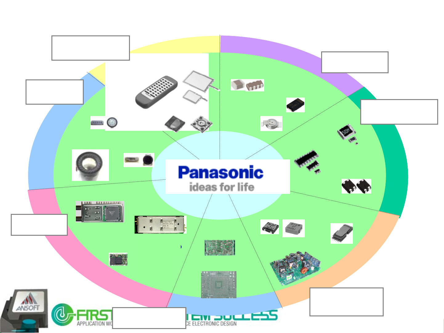
Main Products in PED
Electro-
Mechanical BU
構
機
リモコン
部
品
タッチパネル
MLCC
コン
デ
ン
サ
Capacitor G
Speaker BU
ピー
ス
Module BU
マイクロス ピーカ
カ
チタンドームスピーカ
デジタルチュー ナ
モ
ジ
Bluetooth SDIO-11b
ュ
ー
ル
ライトタッチスイッチ
レシーバ
基地局モジュー ル
電気二重層
コンデンサ
多層基板
ALIVH
機能性コンデンサ
チップR(アレイ)
パワーチョークコイル
電源ユ ニット
チップR
コモンモ ード
ノイズフィルタ
インバータトランス
・
Circuit
Components BU
回
路
部
品
器
Printed Circuit
Board BU
回
路基
板
変成
Inductive
Products BU
Page 5
Global production and R&D base list
PEDTJ
PTCC
●
■
●
●
PEDUK
PEDEU
PEDEU-TC
PEDEU-SK
PEDTH
MAPREC
PEDMA
MEDEM
PEDSG
PEDSG-ST
PEDHK
PEDJM
●
●
●●
●
■
●
●
◆◆
●
●
◆
▲
■
▲
◆
PEDBJ
PEDCBJ
PEDQD
●
PTW
PMX
PEDCA
PEDCA-TC
■
●
●
PEDCA-BC
P E D
P E D
●
PEDCA-TA
●
● Electronic part special producing company 16
▲ Part overseas production business place 2
◆ Joint venture company 4
■ R&D base 4
PACOB-AM
PEDSG-BT
PEDIDA
Page 6

LCR Solution on PED WEB Site
http://panasonic.co.jp/ped/
http://panasonic.co.jp/ped/
Device Library
・・・Data
・・・Data
s
for
for
Suppression Solutions
・・・
・・・
SMD Capacitor Selection Guide
・・・
・・・
imulation
s
imulation
Device selection guide
Device selection guide
Device selection guide
Device selection guide
Library
Library
Page 7
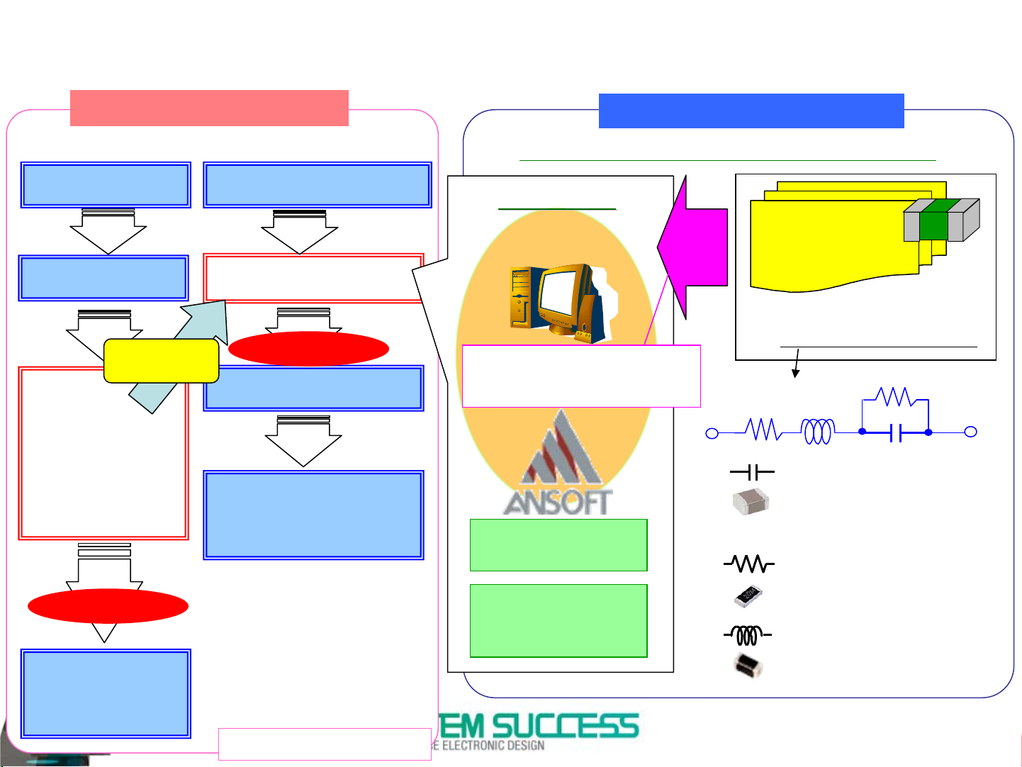
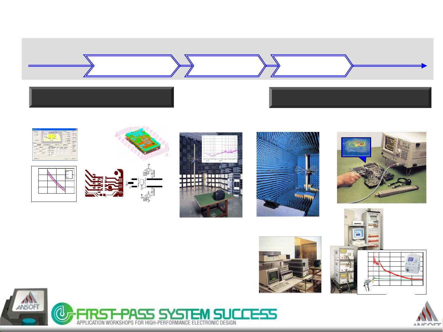
Purpose of Device Library
Customer/Set
【Conventional】 【Current】
Catalog retrieval
Sample order
Shortening
Circuit design and
Experimental
evaluation
Device selection
Experimental
evaluation
Catalog retrieval on WEB
Circuit design(simulation)
Device selection
Sample order on WEB
Experimental
evaluation
PED/Device
http://industrial.panasonic.com/i/library.html
Simulator
Simulator
High frequency circuit & system
design tool
Please downloads from Web
and registers it as a component
for the simulator.
Improvement of
design perfection
Efficiency
improvement of
design
C
C
R
R
L
L
Device
Device
Parameter
Parameter
S Parameter
Equivalent circuit model
例) Capacitor
●Chip multi-layer
ceramic capacitors
<MLCC’s>
(270 parts numbers)
●Chip resistors
(186 parts numbers )
●Chip inductors
(45 parts
numbers )
Circuit design process
Page 8
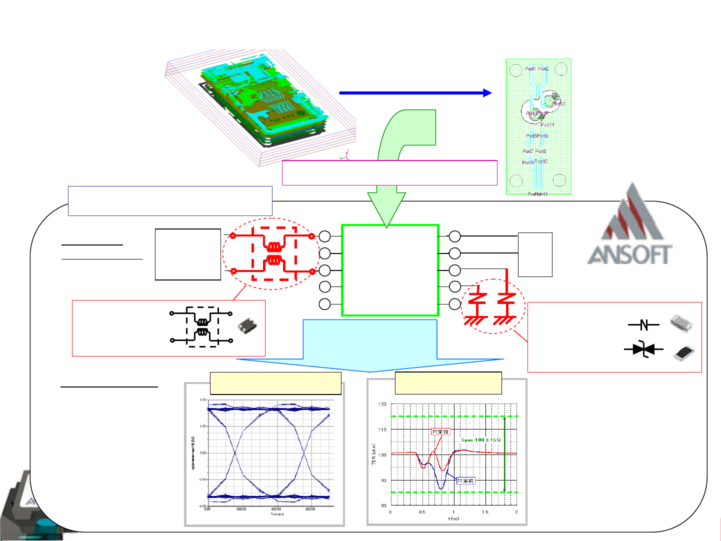
Simulation analysis with substrate CAD data and Device Library
Evaluation block
cutting out
Material constant setting
Substrate CAD data
Electromagnetic field analysis
Circuit simulation
Simulation
block diagram
Connector
S parameter
of circuit board
IC
Device LibraryDevice Library
Common
mode
noise filter
Simulation result
Transmission
characteristic analysis
Eye pattern analysis
Chip varistors
ESD Suppressor
TDR analysis
Page 9
LCR solution activity flow
Plan
Development step of set circuit design
Making
for trial purposes
Selection of the
Simulation
best parts
Device selection and recommended
pattern proposal
Electromag
netic field
analysis
60
55
50
Z(Ohm)
45
40
100 150 200 250 300
Line Width (um)
4.2
4.4
4.6
Impedance
design
Circuit simulation
①Solution corresponding to design phase
②Total solution with a lot of devices
Radiation obstruction
wave measurement
Conduction obstruction wave
voltage measurement
EvaluationCircuit design
Noise evaluation at EMC Site
Electromagnetic radiate
field immunity
examination
Mass
production
Analysis by
electromagnetic field
probe
Radio
frequency
conduction
obstruction
1200
1000
800
600
)
400
Volts (V )
電圧
(V
200
0
-200
-20 20 60 100 140 180
examination
0
Tim e s (nS e c s )
時間
(nSec)
Page 10

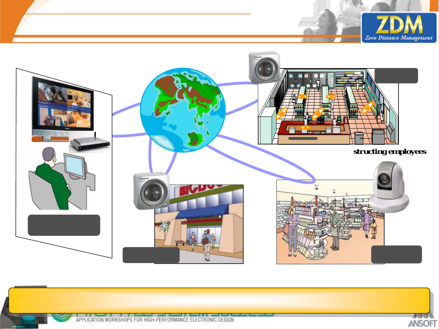
Remote IP Monitoring
Demand of Remote IP Monitoring
I want to monitor my branch
shops at any time, any place.
(Franchise retail store owner)
I want to check the present
Condition or change
for large facility.
(Parking lot, warehouse)
I want to check branches to
make sure if everything is fine
(Branch, factory, school)
I want to install Security
system, but expensive!
I need something at
reasonable cost .
I want to make HP
more attractive.
(Live monitoring)
I want to improve customer
satisfaction, energy saving
(Building, apartment, hotel)
Remote IP Monitoring corresponds to such needs!!
Remote IP Monitoring corresponds to such needs!!
10
Page 11
Remote IP Monitoring
ZDM [ Zero Distance Management ]
INTERNET
Multiple- Franchises
Store A
Cashier
Supervising and instructing employees
Multiple- Offices
Owner’s
Home or Office
Store C
Security use at night
Grocery Stores
Store B
Monitoring traffic of visitors
Improve the Quality of Management by IP Monitoring
Page 12

Remote IP Monitoring
ZDM [ Zero Distance Management ]
Remote IP Monitoring
Provides effective solution and benefit
to improve the Quality of Management
•Distance Free!
•High Reliability!
•Save Time & Cost!
•Integration with
IP-PBX, POS, ATM!
Multi Display
PBX
PC
Network
Video Recorder
POS
PC
Network
ATM
12
Page 13

Remote IP Monitoring
Network Camera
Line up
Wireless
BB-HCM580
Zoom
PoE
BB-HCM581
BB-HCM511
BB-HCM531
Out Door
BB-HCM515
BL-C131
In Door
BL-C111
Pan/Tilt
Page 14

Introducing
Project Definitions
Page 15

Motivation of the Project
• Panasonic to employ Computer Aided
Engineering in their System.
– Time to Market…Initial Design to Product
– Robust Design
• EYE Design
• EMI/EMC Regulation
• Establish the methodology of designing
products using Simulator instead of Cut
and Try method.
Page 16

Why not Cut and Try?
• If Engineer is lucky, then it will probably find
solution quickly modifying the design.
• It all depends on the engineer’s skill and
experiences.
• Just making the prototype board takes 2 months
and measurements takes additional one month.
• CAE based approach not just reveal all the
problems but also gives path to greatly
enhance their products.
Page 17

Ansoft Tools ready to Solve their
requirements?
• LVDS system in Network Camera is huge. No
Electromagnetic Simulator can possibly solve the entire
problem.
• Ansoft has suggested to use combination of
Electromagnetic Simulator as well as Circuit
Simulator to find the causes of their prototype board.
• PED/PCC/Molex Japan together with Ansoft formed
project to establish design flow using prototype boards.
(System and Boards which failed.)
• Knowledge and experiences obtained through this
project has been implemented in Panasonic for future
products.
Page 18

Project Scope
LVDS TxTx
LVDS
LVDS
TX
[d B (μ V /m)]
Maintain Quality Eye Diagram
60
50
40
基板
基板
コ
ネ
FPC
ク
タ
コ
ネ
ク
タ
中継基板
中継基板
LVDS差動ライン
Suppress Radiation Noise (EMI/EMC)
Implication is to reduce Common Mode Degeneration
through out the system
30
レベル
20
LVDS Rx
LVDS Rx
コ
ネ
ク
タ
FFC
コ
ネ
ク
タ
基板
基板
LVDS
Rx
10
0
30 100050 100 500
周波数
[M H z]
Page 19

Approaches to the
Project
LVDS TxTx
LVDS
LVDS
TX
基板
基板
LVDS Rx
中継基板
中継基板
コ
ネ
FPC
ク
タ
コ
ネ
ク
タ
LVDS差動ラ
イン
コ
ネ
FFC
ク
タ
LVDS Rx
コ
ネ
ク
タ
基板
基板
LVDS
Rx
Duplicate the System in Simulation
Match to the Measurements if available
Use the system to improve the performance
Page 20

LVDS TxTx
LVDS
基板
基板
中継基板
中継基板
LVDS Rx
LVDS Rx
基板
基板
LVDS
TX
Port1
Port2
1
2
SiWave Analysis
HFSS Analysis
コ
ネ
ク
タ
FPC
コ
ネ
ク
タ
LVDS差動
ライン
コ
FFC
ネ
ク
タ
コ
ネ
ク
タ
FPC and Molex Con nectors
VIDEO Board
U2
5
6
VIDEO Board
VIDEO Board
LVDS Tx基板 LVDS Rx基板中継基板
7
8
ref
0
3
4
LVDS FPC and Connector
Port1
FPC and Mol ex Connector
Port2
PlanarEM
Nexxim W-element
Port3
Port4
1
2
5
6
TILT Board
T ILT Board CPU Bo a rd
SiWave Analysis
HFSS Analysis
ref
0
LVDS
Rx
FFC and Mol ex Connectors
U11
FFC and Connector
7
8
3
Port1
Port2
4
FFC and Molex Connector
PlanarEM
Nexxim W-element
Port3
Port4
1
2
5
6
CPU Boa rd
7
8
ref
0
3
Port3
4
Port4
SiWave Analysis
HFSS Analysis
FFC Mid Secti on
Port1
Port2
n4
n3
ref
0
3
4
0
n2
n1
0
1
2
n2
n1
U2
seg1
Port1
Port5
n5
n6
Port2
Port6
Port3
Port7
n7
n8
Port4
Port8
U4
seg2
n4
n3
Port1 Port2
1
2
0
n5
n6
Port3 Port4
Port5 Port6
n7
n8
Port7 Port8
Port3
ref
0
3
4
Port4
Port1
Port2
FFC
n1
3
4
n3 n4
ref
n5
1
2
n7
FFC
n2
n6
n8
n2
n2
n1
n1
n3 n4
n4n3
n5
n5
n6
n7
n7
n8
1
2
Port3
ref
n6
3
4
n8
Port4
Page 21

Port2
Port1
Examine Total System
FPC and Molex Con nectors
U2
1
2
5
6
VIDEO Board
VIDEO Board
LVDS Tx基板 LVDS Rx基板中継基板
7
8
ref
0
3
4
LVDS FPC and Connector
Port1
FPC and Mol ex Connector
Port2
Port3
Port4
1
2
5
6
TILT Board
T ILT Board CPU Bo a rd
FFC and Mol ex Connectors
U11
FFC and Connector
7
8
ref
0
3
Port1
Port2
4
FFC and Molex Connector
Port3
Port4
1
2
5
6
CPU Boa rd
7
8
ref
0
3
Port3
4
Port4
Ansoft Corporation LVDS TDR folded
150.00
140.00
130.00
120.00
110.00
100.00
-V(Diff1)/I(Diff1)
90.00
80.00
70.00
We may want to do
60.00
Impedance
Transient
something
50.00
0.00 1.00 2.00 3.00 4.00 5.00 6.00 7.00 8.00 9.00 10.00
for this
Tim e [ns]
Curve Inf o
-V(Diff1)/I(Diff1)
Page 22

LVDS TxTx
LVDS
基板
基板
中継基板
中継基板
LVDS Rx
LVDS Rx
基板
基板
LVDS
TX
コ
ネ
ク
タ
FPC
コ
ネ
ク
タ
LVDS差動ラ
イン
LVDX Tx Board
コ
ネ
FFC
ク
タ
コ
ネ
ク
LVDS
Rx
タ
Ansoft Corporation VIDEO board
0.00
-20.00
-40.00
XY Plot 1
0~8GHz
-60.00
Y1
-80.00
-100.00
-120.00
0.00 1.00 2.00 3.00 4.00 5.00 6.00 7.00 8.00
F [GHz]
Curv e Inf o
dB(S(Port1,Port1))
LinearFrequency
dB(S(Port1,Port2))
LinearFrequency
dB(S(Port1,Port3))
LinearFrequency
dB(S(Port1,Port4))
LinearFrequency
dB(S(Port1,Port5))
LinearFrequency
dB(S(Port1,Port6))
LinearFrequency
dB(S(Port1,Port7))
LinearFrequency
dB(S(Port1,Port8))
LinearFrequency
dB(S(Port2,Port1))
LinearFrequency
Page 23

Video Board Time Domain
Ans oft Corporation LVDS TDR folded
150.00
140.00
130.00
Impedance
Curve Inf o
-V(Diff1)/I(Diff1)
Transient
• It is a little high
120.00
• Needs to investigate for the thickness of the board
112Ω
110.00
100.00
-V(Diff1)/I(Diff1)
90.00
80.00
Pad
70.00
Via
60.00
50.00
0.00 1.00 2.00 3.00 4.00 5.00 6.00 7.00 8.00 9.00 10.00
Tim e [ns ]
Page 24

~100Ω Differential Line
May cause Skew if the components are placed.
~54Ω Differential Line
Page 25

LVDS TxTx
LVDS
基板
基板
中継基板
中継基板
LVDS Rx
LVDS Rx
基板
基板
LVDS
TX
コ
ネ
ク
タ
FPC
コ
ネ
ク
タ
LVDS差動ラ
イン
Molex (25435-2771)
FPC
Port2
Port1
n2
n1
1
2
ref
3
4
0
n4
n3
n5
0
0
n6
n7
n8
Port1
Port5
Port3
Port7
U2
seg1
Port2
Port6
Port4
Port8
n2
n1
n4
n3
n6
n8
W-Element W-Element
コ
ネ
ク
タ
Port1 Port2
n5
Port3 Port4
Port5 Port6
n7
Port7 Port8
FFC
U4
seg2
コ
ネ
ク
LVDS
Rx
タ
1
0
0
2
ref
3
4
Port3
Ansoft Corporation LVDS Signal Pass
Name X Y
m1 257.0000 -2.5648
0.00
-20.00
-40.00
-60.00
Y1
-80.00
-100.00
-120.00
0.00 100.00 200.00 300.00 400.00 500.00
XY Plot 1
Port4
m1
F [MHz]
LinearFrequency
LinearFrequency
LinearFrequency
LinearFrequency
LinearFrequency
LinearFrequency
LinearFrequency
LinearFrequency
LinearFrequency
LinearFrequency
LinearFrequency
LinearFrequency
LinearFrequency
LinearFrequency
LinearFrequency
Curve In f o
dB(S(Port1,Port1))
dB(S(Port1,Port2))
dB(S(Port1,Port3))
dB(S(Port1,Port4))
dB(S(Port2,Port1))
dB(S(Port2,Port2))
dB(S(Port2,Port3))
dB(S(Port2,Port4))
dB(S(Port3,Port1))
dB(S(Port3,Port2))
dB(S(Port3,Port3))
dB(S(Port3,Port4))
dB(S(Port4,Port1))
dB(S(Port4,Port2))
dB(S(Port4,Port3))
Page 26

FPC Straight and Bobbin effect
Ansoft Corporation LV DS TDR
150.00
140.00
130.00
120.00
110.00
100.00
-V(Diff1)/I(Diff1)
90.00
80.00
70.00
60.00
50.00
0.00 1.00 2.00 3.00 4.00 5.00 6.00 7.00 8.00 9.00 10.00
Loose Winding
Single Layer FPC
Impedance
Transient
Curv e Info
-V(Diff1)/I(Diff1)
Measurement stays in this range
Time [ns]
LVDS TxTx
LVDS
基板
基板
LVDS
TX
Ansoft Corporation LVDS TDR folded
-V(Diff1)/I(Diff1)
~15Ω
コ
ネ
ク
タ
150.00
140.00
130.00
120.00
110.00
100.00
90.00
80.00
70.00
60.00
50.00
0.00 1.00 2.00 3.00 4.00 5.00 6.00 7.00 8.00 9.00 10.00
Tight Winding
Multi-Layer FPC
中継基板
中継基板
コ
FPC
ネ
ク
LVDS差動ラ
タ
Impedance
Time [ns]
コ
ネ
ク
タ
FFC
LVDS Rx
LVDS Rx
コ
ネ
ク
タ
Transient
イン
Curv e Info
-V(Diff1)/I(Diff1)
LVDS
Rx
基板
基板
Page 27

LVDS TxTx
LVDS
基板
基板
中継基板
中継基板
LVDS Rx
LVDS Rx
基板
基板
LVDS
TX
コ
ネ
ク
タ
FPC
コ
ネ
ク
タ
LVDS差動ラ
コ
ネ
FFC
ク
タ
コ
ネ
ク
LVDS
Rx
タ
イン
TILT Board
Ansoft Corporation TILT board
0.00
-10.00
-20.00
-30.00
Y1
-40.00
-50.00
-60.00
-70.00
0.00 1.00 2.00 3.00 4.00 5.00 6.00 7.00 8.00
XY Plot 1
F [GHz]
Cur v e Inf o
dB(S(Port1,Port1) )
LinearFrequency
dB(S(Port1,Port2) )
LinearFrequency
dB(S(Port1,Port3) )
LinearFrequency
dB(S(Port1,Port4) )
LinearFrequency
dB(S(Port2,Port1) )
LinearFrequency
dB(S(Port2,Port2) )
LinearFrequency
dB(S(Port2,Port3) )
LinearFrequency
dB(S(Port2,Port4) )
LinearFrequency
dB(S(Port3,Port1) )
LinearFrequency
dB(S(Port3,Port2) )
LinearFrequency
dB(S(Port3,Port3) )
LinearFrequency
Page 28

TILT Board Time Domain
Ans oft Corporation LVDS TDR folded
150.00
140.00
130.00
120.00
110.00
100.00
-V(Diff1)/I(Diff1)
90.00
80.00
TILT
70.00
60.00
50.00
0.00 1.00 2.00 3.00 4.00 5.00 6.00 7.00 8.00 9.00 10.00
VIA
Impedance
Ansoft Corporation LVDS TDR
150.00
140.00
130.00
120.00
110.00
100.00
-V(Di ff1)/I(Diff1 )
90.00
80.00
70.00
60.00
50.00
Tim e [ns]
Curv e Info
-V(Diff1)/I(Diff 1)
Transient
Impedance
TILT 0~2GHz
Transient
Transient
Curv e Info
-V(Diff1)/I(Diff 1)
-V(Diff1)/I(Diff 1)
TILT 0~8GHz
0.00 1.00 2.00 3.00 4.00 5.00 6.00 7.00 8.00 9.00 10.00
Time [ns ]
Page 29

LVDS TxTx
LVDS
基板
基板
中継基板
中継基板
LVDS Rx
LVDS Rx
基板
基板
Port2
Port1
LVDS
TX
コ
ネ
ク
タ
FPC
コ
ネ
ク
タ
LVDS差動ラ
コ
ネ
FFC
ク
タ
コ
ネ
ク
LVDS
Rx
タ
イン
Molex Connector
FFC
n2
n6
n8
n1
n5
n7
FFC Mid Section
FFC
n2
n1
n3 n4
n4n3
n5
n6
n7
n8
n2
n6
n8
1
2
ref
3
4
Port3
Port4
FFC
n1
3
4
ref
1
2
n3 n4
n5
n7
Page 30

FFC Geometry
B1:5±1.5
B2:5±1.5
M:0.5±0.1
Page 31

PQJE10183XA-SV.pdf
B1:5±1.5
.layerstack FFC_edge
+ layer = (air, 'Air_thickness'),
+ layer = (Base, 188um) ,
+ layer = (Polyester, 40um) ,
+ layer = (Base, 'FFC_Base_Thickness') ,
+ layer = (Polyester, 'FFC_polyester_Thickness+FFC_Conductor_Thickness') ,
+ layer = (air, 'Air_thickness+FFC_polyester_Thickness+FFC_Base_Thickness')
B2:5±1.5
M:0.5±0.1
.layerstack FFC_mid
+ layer = (air, 'Air_thickness+188um+40um'),
+ layer = (Base, 'FFC_Base_Thickness') ,
+ layer = (Polyester, '2*FFC_polyester_Thickness+FFC_Conductor_Thickness') ,
+ layer = (Base, 'FFC_Base_Thickness') ,
+ layer = (air, 'Air_thickness')
Page 32

B1:5±1.5
PQJE10183XA-SV.pdf
B2:5±1.5
M:0.5±0.1
Port2
Port1
n2
n6
n8
n1
n5
n7
FFC Mid Section
FFC
n2
n1
n3 n4
n4n3
n5
n6
n7
n8
n2
n6
n8
1
2
ref
3
4
Port3
Port4
FFC
n1
3
4
ref
1
2
n3 n4
n5
n7
Page 33

FFC Time Domain
Ans oft Corporation LVDS TDR folded
150.00
Impedance
Curv e Info
-V(Dif f 1)/I(Dif f 1)
Transient
140.00
FFC Mid Sectio n
FFC
n2
n1
Port1
3
4
Port2
ref
1
2
n3 n4
n5
n7
n1
n5
n6
n7
n8
n2
n1
n3 n4
n4n3
n5
n6
n7
n8
FFC
n2
n6
n8
1
2
Port3
ref
3
4
Port4
130.00
120.00
110.00
100.00
-V(Diff1)/I(Diff1)
90.00
80.00
70.00
60.00
50.00
0.00 1.00 2.00 3.00 4.00 5.00 6.00 7.00 8.00 9.00 10.00
Tim e [ns]
Page 34

LVDS TxTx
LVDS
基板
基板
中継基板
中継基板
LVDS Rx
LVDS Rx
基板
基板
LVDS
TX
コ
ネ
ク
タ
FPC
コ
ネ
ク
LVDS差動ラ
タ
コ
ネ
FFC
ク
タ
イン
LVDS Rx Board
Ansoft Corporation CPU
0.00
-20.00
-40.00
XY Plot 1
コ
ネ
ク
LVDS
Rx
タ
-60.00
Y1
Curv e Inf o
dB(S(Port1,Port1))
-80.00
-100.00
-120.00
0.00 0.50 1.00 1.50 2.00
F [GHz]
LinearFrequency
dB(S(Port1,Port2))
LinearFrequency
dB(S(Port1,Port3))
LinearFrequency
dB(S(Port1,Port4))
LinearFrequency
dB(S(Port1,Port5))
LinearFrequency
dB(S(Port1,Port6))
LinearFrequency
Page 35

LVDS System Review
FPC and Molex Con nectors
U8
Port1
Port2
Ansoft Corporation LVDS S y s tem
10.00
0.00
-10.00
-20.00
-30.00
Y1
-40.00
-50.00
-60.00
1
2
5
6
VIDEO Board
LVDS Tx基板 LVDS Rx基板中継基板
VIDEO Board
7
8
ref
3
4
XY Plot 1
FPC and Connector
Port1
FPC and Mol ex Connector
Port2
Port3
Port4
Curv e Inf o
dB(S(Port1,Port1))
LinearFrequency
dB(S(Port1,Port2))
LinearFrequency
dB(S(Port1,Port3))
LinearFrequency
dB(S(Port1,Port4))
LinearFrequency
dB(S(Port2,Port1))
LinearFrequency
dB(S(Port2,Port2))
LinearFrequency
1
2
FFC and Molex Con nectors
U7
FFC and Connector
FFC and Molex Connector
Port3
Port4
1
2
5
6
CPU Board
7
8
ref
3
4
5
6
TILT Board
7
8
ref
3
Port1
Port2
4
TILT Board CPU Bo a rd
Ansoft Corporation LVDS TDR folded
150.00
140.00
130.00
120.00
110.00
100.00
-V(Diff1)/I(Diff1)
90.00
80.00
70.00
60.00
Im pedance
Port3
Transient
Curv e Inf o
-V(Diff1)/I(Diff1)
Port4
-70.00
0.00 0.50 1.00 1.50 2.00
F [GHz]
50.00
0.00 1.00 2.00 3.00 4.00 5.00 6.00 7.00 8.00 9.00 10.00
Tim e [ns ]
Page 36

Improving the
Ansoft Corporation LVDS TDR folded
150.00
140.00
Impedance
Transient
Curv e Info
-V(Diff1)/I(Diff1)
Design
130.00
120.00
110.00
100.00
-V(Diff1)/I(Diff1)
90.00
80.00
70.00
60.00
50.00
0.00 1.00 2.00 3.00 4.00 5.00 6.00 7.00 8.00 9.00 10.00
• VIDEO Board
• FPC Board
• Impedance matching through the FPC line
Tim e [ns ]
• Impedance matching and Skew Reduction in VIDEO Board
– EYE Design and Reduction of Differential to Common Mode
Page 37

Improving
Impedance Matching on the
FPC
Ansoft Corporat ion LVDS TDR folded
150.00
140.00
130.00
120.00
110.00
100.00
-V(Di ff1)/I(Diff1)
90.00
80.00
70.00
60.00
50.00
0.00 1.00 2.00 3.00 4.00 5.00 6.00 7.00 8.00 9.00 10.00
Impedance
Time [ns]
Transient
Curv e Inf o
-V(Diff1)/I(Diff1)
Page 38

Polyamide Sheet
Matching FPC
By placing Polyamide sheet on top of FPC, Electromagnetic
fields are captured in the vicinity of the Differential Line.
Hence the Capacitor increase resulting to decrease the
Characteristic impedances
Ansoft Corporation LVDS TDR folded
150.00
140.00
130.00
120.00
110.00
100.00
-V(Di ff1)/I(Di ff1)
90.00
Impedance
Transient
Curv e Inf o
-V(Diff1)/I(Diff1)
80.00
70.00
60.00
50.00
0.00 1.00 2.00 3.00 4.00 5.00 6.00 7.00 8.00 9.00 10.00
Tim e [ns ]
Page 39

Finding Characteristic
Impedance in Frequency Domain
Use Open/Short conditions
to compute the Impedances
By selecting the transformer
ratio, differential impedance
can be computed by
Zo=sqrt(Zopen*Zshort)
Open
1
0
Short
1
0
2
3
2
3
R220
R225
25
25
n1
0
n3 n4
0
0
n5
n7
0 0
n1
0
n3 n4
n5
n7
n2
n2
n6
n8
n6
n8
00
Page 40

Matching FPC Impedance
Ansoft Corporat i on FPC Impr ove
150.00
140.00
130.00
120.00
Polyamide Sheets
On both side
Ansoft Corporation LVDS TDR folded with modified FPC
140.00
130.00
120.00
110.00
100.00
90.00
-V(Diff1)/I(Diff1)
80.00
70.00
Reduce portion of FPC
60.00
impedance Mismatch
50.00
1.00 2.00 3.00 4.00 5.00 6.00 7.00 8.00 9.00 10.00
Impedance
Time [ns]
110.00
100.00
90.00
Curv e Inf o
mag(sqrt(Z(Open,Open)*Z(Short,Short)))
-V(Diff 1)/I(Diff1)
Transient
80.00
70.00
60.00
50.00
0.00 1.00 2.00 3.00 4.00 5.00 6.00 7.00 8.00
XY Plot 1
Curve Info
mag(sqrt(Z(Open,Open)*Z(Short,Short)))
LinearFrequency
75um Polyamide sheets on both
side of FPC
*=============================================
.param FPC_Base=25.4um
.param FPC_Conductor=35um
.param Air_thickness=800um
.param FPC_Thickness='Air_thickness+3*FPC_Base'
.param FPC_Thickness_stacked='Air_thickness+(2*FPC_Base+FPC_Conductor)+FPC_Base'
*=============================================
.layerstack FPCBoard
+ layer = (air, 'Air_thickness'),
+ layer = (Polymide, '6*FPC_Base+FPC_Conductor') ,
+ layer = (air, 'Air_thickness')
F [GHz]
Page 41

Covering with Polyamide Sheets
Ansoft Cor po ra tion LVDS TDR folded w i th mod i fi e d F PC
140.00
130.00
120.00
110.00
100.00
90.00
-V(Diff1)/I(Diff1)
80.00
70.00
60.00
50.00
1.00 2.00 3.00 4.00 5.00 6.00 7.00 8.00 9.00 10.00
Impedance
Time [ns]
Curve Info
Transient
-V(Diff 1)/I(Diff1)
Ansoft Corporation LVDS TDR folded with modified FPC
140.00
130.00
120.00
110.00
100.00
90.00
-V(Diff1)/I(Diff1)
80.00
70.00
60.00
50.00
1.00 2.00 3.00 4.00 5.00 6.00 7.00 8.00 9.00 10.00
Impedance
Time [ns]
Curve Info
-V(Diff1)/I(Diff1)
Transient
Page 42

Improving
Impedance Matching
and
Skew
on the LVDS Tx board
Page 43

Skew and Impedance Matching
on LVDS Tx Board
Skew
Matching
Strategy
Ansoft Corporation LVDS TDR folded
150.00
140.00
130.00
120.00
110.00
100.00
-V(Diff1)/I(Diff1)
90.00
80.00
70.00
60.00
50.00
0.00 1 .00 2.00 3.00 4.00 5.00 6.00 7.00 8.00 9.00 10.00
Impedance
Time [ns]
Transient
Curve Info
-V(Diff1)/I(Diff1)
Change size of Ground Hall
Impedance Matching Strategy
Page 44

Crossed Dual Via Model in HFSS
LumpPort1:1
LumpPort2:1
Port2
Port1
LumpPort3:1
Port3
LumpPort4:1
ref
0
Port4
Nexxim Dynamic Link to HFSS
Sweep on the parameters on the HFSS
Ansoft Corporation Cros s Dual Vi a
0.00
-0.02
-0.04
-0.06
dB(S(Port3,Port1))
-0.08
-0.10
-0.12
-0.14
0.00 0.50 1.00 1.50 2.00 2.50 3.00 3.50 4.00
XY Plot 1
keepout=300um
keepout=400um
keepout=500um
keepout=600um
F [GHz]
Curv e Inf o
dB(S(Port3,Port1))
dB(S(Port3,Port1))
dB(S(Port3,Port1))
dB(S(Port3,Port1))
Keepout
Keepout
radius=400~500um gives the maximum transfer through the
radius=400~500um
Frequency range of 0~4GHz
Page 45

Layout Design using PlanarEM
in Ansoft Designer 4.0
Port2
Port1
Ansoft Corporati on Modified VIDEO Board 070707
0.00
-10.00
-20.00
-30.00
-40.00
-50.00
Y1
-60.00
Port3 Po rt4
1
2
1
1
2
2
3
4
ref
0
Port3 Port4
Port1
Port2
-70.00
-80.00
-90.00
-100.00
0.00 0.50 1.00 1.50 2.00 2.50 3.00 3.50 4.00
XY Plot 1
F [GHz]
Curve Inf o
dB(S(Vide
LinearFrequency
dB(S(Vide
LinearFrequency
dB(S(Vide
LinearFrequency
dB(S(Vide
LinearFrequency
Page 46

Final Design Modification
450um
350um
300um
Port3 Port4
110um
W=220um
S=150um
Port1
150um
220um
Port2
250m
Page 47

Modified Total System
Modified
U3
Port1
Port2
LVDS Tx基板
Video_in1
Video_in2
Modified VIDEO Board 070707
Modified Video Board
Video_out1
Video_out2
U5
LVDS FPC and Conn ector4
Port1
FPC and Molex Connector
Port2
Port3
1
2
Port4
中継基板
U1
Cross Dual Via
Port1
Port2
4
3
Port4
Port3
1
2
3
1
4
2
ref
0
Ansoft Corporation LVDS S ystem_fol ded_ F P C2
20.00
0.00
-20.00
-40.00
Y1
-60.00
-80.00
-100.00
-120.00
0.00 0.50 1.00 1.50 2.00 2.50 3.00 3.50 4.00
XY Plot 1
F [GHz]
Curve Info
dB(S(Port1,Port1))
LinearFrequency
dB(S(Port1,Port2))
LinearFrequency
dB(S(Port1,Port3))
LinearFrequency
dB(S(Port1,Port4))
LinearFrequency
dB(S(Port2,Port1))
LinearFrequency
dB(S(Port2,Port2))
LinearFrequency
dB(S(Port2,Port3))
LinearFrequency
dB(S(Port2,Port4))
LinearFrequency
dB(S(Port3,Port1))
LinearFrequency
FFC and Molex Connectors
U7
Port1
FFC and Molex Connector
Port2
FFC and C onne ctor4
Port3
Port4
LVDS Rx基板
1
567
2
CPU Board
ref
Ansoft Corporation LVDS TDR folded
150.00
140.00
130.00
120.00
110.00
100.00
-V(Diff1)/I(Diff1)
90.00
80.00
70.00
60.00
50.00
0.00 1.00 2.00 3.00 4.00 5.00 6.00 7.00 8.00 9.00 10.00
567
TILT Bo ard
ref
3
4
8
TILT Board CPU Board
Ansoft Corporation LVDS TDR folded with modified FPC and video board
150.00
140.00
130.00
120.00
110.00
100.00
-V(Diff1)/I(Diff1)
90.00
80.00
70.00
60.00
50.00
0.00 1.00 2.00 3.00 4.00 5.00 6.00 7.00 8.00 9.00 10.00
8
Impedance
Time [ns]
3
Port3
4
Port4
Impedance
Time [ns ]
Transient
Curv e Inf o
-V(Diff1)/I(Diff1)
Transient
Curve Info
-V(Diff1)/I(Diff1)
Page 48

PRBS Simulation
R163
0
50
V159
R164
50
V160
3
4
1
2
ref
0
R151
50
V
0
V
R152
50
0
Measurements
0
Simulation
LVD S RxLVD S Rx基板基板
中継基板中継基板
LVD S LVD S TxTx基板基板
LVD S LVD S TxTx基板基板
コ
コ
ネ
LVDS
LVDS
TX
TX
Ansoft Corpora t ion LVDS with PRBS measurements
2.00
1.50
1.00
0.50
0.00
Vdiff [V]
-0.50
-1.00
-1.50
-2.00
0.00 2.00 4.00 6.00 8.00 10.00 12.00 14.00 16.00
2.00
1.50
1.00
0.50
0.00
Vdiff [V]
-0.50
-1.00
-1.50
-2.00
0.00 0.50 1.00 1.50 2.00
ネ
FPC
FPC
ク
ク
タ
タ
中継基板中継基板
コ
コ
ネ
ネ
ク
ク
LVDS差動ラ
LVDS差動ラ
タ
タ
イン
イン
Eye
Time [ns]
Time [us]
コ
コ
ネ
ネ
FFC
FFC
ク
ク
タ
タ
LVD S RxLVD S Rx基板基板
コ
コ
ネ
ネ
ク
ク
タ
タ
LVDS
LVDS
Rx
Rx
Curv e Inf o
Tran sient
Vdiff
Port1
Port2
LVDS Tx基板
Modified Video/FPC
U3
Modified
Modified VIDEO Board 070707
Modified Video Board
1
2
Ansoft Corporation LVDS with P RB S new syste m
2.00
1.50
1.00
0.50
0.00
Vdiff [V]
-0.50
-1.00
-1.50
-2.00
0.00 2.00 4.00 6.00 8.00 10.00 12.00 14.00 16.00
2.00
1.50
1.00
0.50
0.00
Vdiff [V]
-0.50
-1.00
-1.50
-2.00
0.00 0.50 1.00 1.50 2.00
U5
LVDS FPC and Conne ctor4
3
Port1
Port2
4
FPC and M olex C o nn ector
Port3
1
2
Port4
TILT Board CPU Board
中継基板
FFC and Molex Connectors
567
TILT Bo ard
3
4
8
ref
Eye
Time [n s]
Time [u s]
Port1
FFC and Molex Connector
Port2
U7
FFC and Con nector4
Port3
1
2
Port4
LVDS Rx基板
567
CPU Boa rd
ref
8
Curv e Inf o
Transient
3
Port3
Port4
4
Vdiff
Page 49

Output Common Noise
Ansoft Corpora tion LVDS with PRBS measurementsCommon Noise
100.00
80.00
60.00
40.00
20.00
-0.00
Vcom [mV]
-20.00
-40.00
-60.00
-80.00
-100.00
0.00 0.50 1.00 1.50 2.00
Time [u s ]
Curv e Info
Transient
Ansoft Corpora ti on LVDS w i th P RBS n e w systemCommon No i se
Vcom
100.00
90.00
80.00
Curv e Inf o
Trans ient
Vcom
70.00
60.00
50.00
40.00
30.00
20.00
10.00
-0.00
-10.00
Vcom [m V]
-20.00
-30.00
-40.00
-50.00
-60.00
-70.00
-80.00
-90.00
-100.00
0.00 0.50 1.00 1.50 2.00
Time [us]
Trans ient
Curv e Info
dB(Vcom)
R163
0
Ansoft C orp or at ion LVDS with PRBS new system
Name X Y
0.00
m1 20.0000 -55.6890
m2 30.0000 -55.3825
m3 40.0000 -62.7354
m4 50.0000 -58.8138
m5 60.0000 -56.4834
-10.00
m6 70.0000 -54.9845
m7 180.0000 -64.7677
m8 190.0000 -65.2964
m9 200.0000 -64.2190
-20.00
-30.00
-40.00
dB(Vcom)
-50.00
m2
m1
-60.00
-70.00
-80.00
10.00 100.00 1000.00
m3
XY Plot 1
m6
m5
m4
m9
m7
m8
Spectru m [MHz]
V
50
R164
V159
50
V160
0
Ansoft Corporation LVDS with PRBS new system
V
123
ref
0
4
EXC24CE900
V(out1)+V(out2) [mV]
-100.00
100.00
V
R151
90.00
80.00
70.00
60.00
50.00
40.00
30.00
20.00
10.00
-0.00
-10.00
-20.00
-30.00
-40.00
-50.00
-60.00
-70.00
-80.00
-90.00
0.00 50.00 100.00 150.00 200. 00 250.00
V
0
50
R152
50
With CMNF
XY Plot 3
Transient
Time [ns]
Curv e Inf o
V(out1)+V(out2)
Page 50

Ansoft Corporation LVDS wi th P RBS measure mentsCommon Noise
80.00
Original Board
60.00
Curve I nfo
VcomIn
Transient
40.00
20.00
0.00
VcomIn [mV]
-20.00
-40.00
-60.00
-80.00
0.00 50.00 100.00 150.00 200.00 250.00
Ansoft Corporation LVDS with PRBS measurements with beadsCommon Noise
100.00
Ferrite Beads+Original Board
50.00
0.00
VcomIn [mV]
Time [ns]
Curve Info
VcomIn
Transient
-50.00
-100.00
0.00 50.00 100.00 150.00 200.00 250.00
Can achieve Much Quality EYE pattern with
Ansoft Corpora tion LVDS wi th PRBS new systemCommon No i se
80.00
70.00
Modified FPC/VIDEO
CMNF+Modified FPC/VIDEO
60.00
50.00
Lower Common Mode Degeneration!!
40.00
30.00
20.00
10.00
0.00
Vcom [mV]
-10.00
-20.00
-30.00
-40.00
-50.00
-60.00
-70.00
-80.00
0.00 50.00 100.00 150.00 200.00 250.00
Ansoft Corporation LVDS with PRBS new system
100.00
90.00
80.00
70.00
60.00
50.00
40.00
30.00
20.00
10.00
-0.00
-10.00
V(in1)+V(in2) [mV]
-20.00
-30.00
-40.00
-50.00
-60.00
-70.00
-80.00
-90.00
-100.00
0.00 50.00 100.00 150.00 200.00 250.00
XY Plot 4
Time [ns]
Time [ns]
Time [ns ]
Curve In fo
Vcom
Transient
Curve I nfo
V(in1)+V(in2)
Transient
Ansoft Corporation LVDS with PRBS measurements
2.00
1.50
1.00
0.50
0.00
Vdiff [V]
-0.50
-1.00
-1.50
-2.00
0.00 2.00 4.00 6.00 8.00 10.00 12.00 14.00 16.00
2.00
1.50
1.00
0.50
0.00
Vdiff [V]
-0.50
-1.00
-1.50
-2.00
0.00 0.50 1.00 1.50 2.00
Ansoft Corporation LVDS wit h PRBS measurements wi th beads
2.00
1.50
1.00
0.50
0.00
Vdiff [V]
-0.50
-1.00
-1.50
-2.00
0.00 2.00 4 .00 6.00 8.00 10.00 12.00 14.00 16.00
2.00
1.50
1.00
0.50
0.00
Vdiff [V]
-0.50
-1.00
-1.50
-2.00
0.00 50.00 100.00 150.00 200.00 250.00
Ansoft Corporation LVDS with PRBS new system
2.00
1.50
1.00
0.50
0.00
Vdiff [V]
-0.50
-1.00
-1.50
-2.00
0.00 2.00 4.00 6.00 8.00 10.00 12.00 14.00 16.00
2.00
1.50
1.00
0.50
0.00
Vdiff [V]
-0.50
-1.00
-1.50
-2.00
0.00 0.50 1.00 1.50 2.00
Ansoft Corporation LVDS with PRBS new system
2.00
1.50
1.00
0.50
0.00
Vdiff [V]
-0.50
-1.00
-1.50
-2.00
0.00 2.00 4.00 6.00 8.00 10.00 12.00 14.00 16.00
2.00
1.50
1.00
0.50
0.00
Vdiff [V]
-0.50
-1.00
-1.50
-2.00
0.00 50.00 100.00 150.00 200.00 250.00
Eye
Time [ns ]
Time [us ]
Eye
Time [ns ]
Time [ns ]
Eye
Time [ns]
Time [us]
Eye
Time [ns ]
Time [ns ]
Curve In fo
Vdiff
Transi ent
Curve Info
Vdiff
Transient
Curve Info
Transient
Curve In fo
Transient
Ansoft Corporation LVDS with PRBS measurementsCommon Noise
100.00
80.00
60.00
40.00
20.00
-0.00
Vcom [mV]
-20.00
-40.00
-60.00
-80.00
-100.00
0.00 0.50 1.00 1.50 2.00
Ansoft Corporation LVDS with P RB S measurements with be ads
100.00
50.00
0.00
Vcom [mV]
-50.00
-100.00
0.00 50.00 100.00 150 .00 200.00 250.00
Ansoft Corporation LVDS with PRBS new systemCommon Noise
100.00
Vdiff
Vdiff
90.00
80.00
70.00
60.00
50.00
40.00
30.00
20.00
10.00
-0.00
-10.00
Vcom [mV]
-20.00
-30.00
-40.00
-50.00
-60.00
-70.00
-80.00
-90.00
-100.00
0.00 0.50 1.00 1.50 2.00
Ansoft Corporation LVDS with PRB S new s y s t em
100.00
90.00
80.00
70.00
60.00
50.00
40.00
30.00
20.00
10.00
-0.00
-10.00
V(out1)+V(out2) [mV]
-20.00
-30.00
-40.00
-50.00
-60.00
-70.00
-80.00
-90.00
-100.00
0.00 50.00 100.00 150.00 200.00 250.00
Time [us]
XY Plot 1
Time [ns ]
Time [us]
XY Plot 3
Time [ns ]
Curve Info
Vcom
Transient
Curve Inf o
Vcom
Transient
Curve Info
Vcom
Transient
Curve Info
V(out1)+V(out2)
Transient
Page 51

Using Scc21 and EMI?
Diff1
100 Ohm 100 Ohm
D1 D2
Common1
C1 C2
Ansoft Corporation LVDS Scc 1 CMNF
0.00
-5.00
-10.00
-15.00
Y1
-20.00
-25.00
We are currently evaluating the theory and measurements in correlate
25 Ohm
Panasoni c
Mode Transformer
n3
n1
123
EXC24CE900
ref
XY Plot 2
S-pa r ameter
25 Ohm
n2
4
0
Diff2
Common2
n4
the Scc21 and EMI measurements.
-30.00
-35.00
-40.00
-45.00
-50.00
Qualitatively we observed if Scc21 is small, it will make the EMI small.
Curv e Inf o
dB(S(C1,C1))
LinearFrequency
dB(S(C1,C2))
LinearFrequency
dB(S(C2,C1))
LinearFrequency
dB(S(C2,C2))
LinearFrequency
0.00 0.00 0.01 0.10 1.00
F [GHz]
25 Ohm
Diff 2
Common2
n4
Dif f1
100 Ohm 100 Ohm
D1 D2
Common1
C1 C2
Ansoft Corporation LVDS S cc 2 CM NF
0.00
-5.00
-10.00
-15.00
-20.00
-25.00
Y1
-30.00
-35.00
-40.00
-45.00
-50.00
0.00 0.00 0.01 0.10 1.00
Panasonic
Mode Transformer
25 Ohm
n3
n1
EXC24CE900
XY Plot 2
LinearFrequency
LinearFrequency
LinearFrequency
LinearFrequency
S-pa ramet e r
123
Curv e Inf o
dB(S(C1,C1))
dB(S(C1,C2))
dB(S(C2,C1))
dB(S(C2,C2))
F [GHz]
4
EXC24CE900
ref
0
n2
Page 52

Measurement on EMI
OLD VIDEO BOARD+FPC-A
NEW VIDEO BOARD+FPC-B
+ CMNF on TILT Board
FPC+Board
FPC + Video Board suppress
Noise around 100MHz-180MHz
CMNF
By suppressing the common mode degeneration, we have suppressed the EMI
Noise. Confirmed on the LAB.
Page 53

Designing quality signal line
with Less Common Mode
Degeneration
• Impedance matching (either from frequency domain and TDR) will
result in keeping the quality signal through out the system.
• Skew Reduction through out the System will reduce Common
Mode Degeneration.
• CMNF achieves additional reduction of the Common Mode Noise.
• EMI measurements are done by Panasonic and new
Board+FPC+CMNF reduced all the unnecessary noise from the
system.
• New System maintain good Eye Pattern and Low EMI.
• Electromagnetic Simulator together with Accurate Circuit
Simulator are the key of pin pointing the cause of the problems
Page 54

Acknowledgements
• We like to express deep acknowledgements to
Mr. Higashtiani (PED) for providing all the
precious data to confirm on the Measurements
and Simulation comparison.
• Mr. Kihara and Mr. Suto (PCC) for providing us
prototype board as well as new board. Also all
the effort of making EMI measurements.
• Mr. Noda (Molex Japan) for providing us the
connector models and S-parameters with helpful
discussions.
 Loading...