

Page 1
Technical Guide
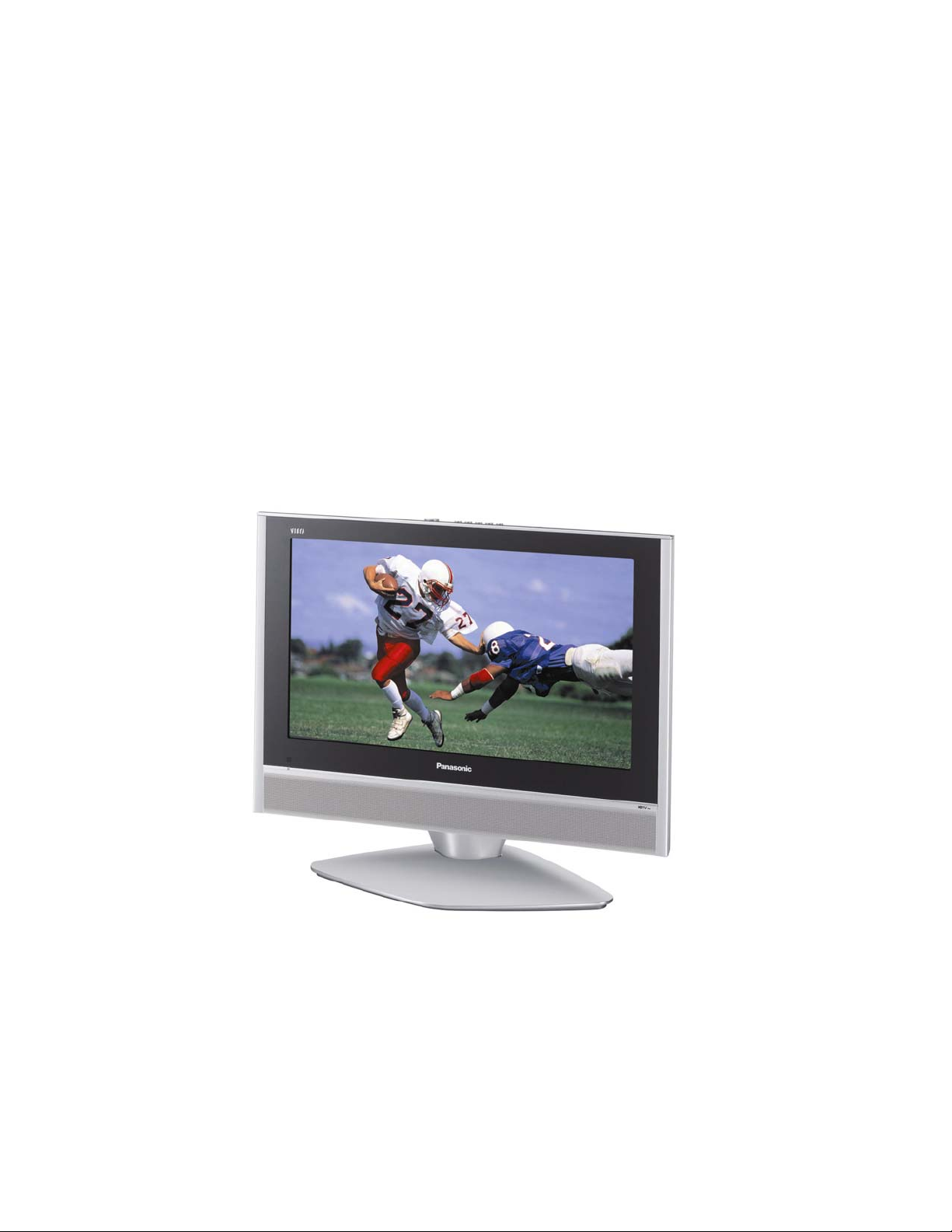
LCD High Definition TV
Models, TC-26LX20, TC-32LX20 and
Combo Model TC-22LR30
LH-34 Chassis
Functional Overview, Circuit Description and
PASC050803TG1
B19
Troubleshooting
Panasonic Services Company
National Training
Page 2

A
y
Prepared by
Gerry Gaimo and Jean Magloire
Panasonic Services Company
National Training
"HDMI, the HDMI logo and High-Definition Multimedia Interface are trademarks or registered trademarks of HDMI Licensing LLC."
BBE, the BBE logo, Sonic Maximizer and High Definition Sound are registered trademarks or trademarks of BBE Sound, Inc.
Copyright © 2005 by Panasonic Services Company
ll rights reserved. Unauthorized copying and distribution is a violation of law.
Warning
This service information is designed for experienced repair technicians only and is not designed for use b
the general public. It does not contain warnings or cautions to advise non-technical individuals of potential
dangers in attempting to service a product. Products powered by electricity should be serviced or repaired
only by experienced professional technicians. Any attempt to service or repair the product or products
dealt with in this service information by anyone else could result in serious injury or death.
Page 3

Table of Contents
Objective........................................................................................................................1
Features.........................................................................................................................2
LCD Technology............................................................................................................ 2
Dynamic Image Balancing............................................................................................3
3D Y/C Separation......................................................................................................... 3
LCD High Definition TV Model Differences.................................................................4
Differences between Models........................................................................................4
Circuit Board Layout.....................................................................................................5
TC-22LR30 Circuit Boards............................................................................................5
Circuit Board Interconnection...................................................................................... 6
System Control Block...................................................................................................7
A Board (TC-22LR30)....................................................................................................9
H Board (TC-26/32LX20) .............................................................................................10
K board (TC-22LR30, TC-26/32LX20)......................................................................... 11
A Board (TC-26/32LX20) .............................................................................................12
Power Supply ..............................................................................................................13
Power Supply (TC-22LR30) ........................................................................................13
P Board - Primary Power......................................................................................... 14
AP Board - Secondary Power.................................................................................15
Tuner / FIP Power Supply (AP Board)....................................................................16
Over Current Protection Shutdown Circuits .........................................................17
14-Volt Power Down Detect Circuit........................................................................18
Over Voltage Protection _ AC Shutdown Latch Circuit .......................................... 19
Power Supply (TC-26/32LX20)....................................................................................20
P board (TC-32LH, TC-26/32LX20) - Primary Power.............................................20
Page 4

Standby Power Supply............................................................................................21
Primary Power Supply............................................................................................. 21
Power Supply Operation (TC-32LH, TC-26/32LX20).............................................. 22
Power On Operation of the DC-to- DC converter..................................................22
Power Off Operation of the DC-to-DC converter...................................................23
Protection of the DC-to-DC converter....................................................................23
AP Board - Secondary Power Supply ....................................................................25
Secondary Voltages...............................................................................................26
Video Circuit Explanation...........................................................................................27
A Board........................................................................................................................27
DG Board .....................................................................................................................28
Video Signal Processing ............................................................................................ 28
Video Signal Processing ............................................................................................ 29
Low Voltage Differential Signaling............................................................................30
HDMI Signal Path.........................................................................................................32
Self-Check Function for TV Section .......................................................................... 33
Self-Check Access...................................................................................................... 33
Servicing the TV Portion.............................................................................................34
Service Adjustment Mode for TV............................................................................34
How to exit Adjustment mode.................................................................................35
Servicing the DVD....................................................................................................... 36
Shutdown Problems.................................................................................................... 38
LED Flashes Three Times .....................................................................................38
LED Flashes Once every 5 seconds......................................................................39
LED Flashes Five Times........................................................................................39
LED Flashes Eight Times.......................................................................................39
Unit shuts down and the Power on LED is off........................................................39
SOS Shutdown Problem........................................................................................39
Does Not Record Video to Disc .................................................................................42
Does Not Record Audio to Disc................................................................................. 43
Primary Power Supply Check ....................................................................................44
Secondary Power Supply Check ............................................................................... 45
Page 5

Appendix......................................................................................................................46
Backlighting................................................................................................................. 46
Inverter Power Supply ................................................................................................46
High Voltage Power Supply........................................................................................ 47
Test and Measurement ............................................................................................... 48
Specifications.............................................................................................................. 49
Combo Overall Specification .....................................................................................49
TV Portion....................................................................................................................50
DVD Portion.................................................................................................................51
Page 6

Objective
This technical guide was prepared with the following objectives in mind:
• Provide the servicer with a brief overview of the concepts of operation for new
circuits employed in this line of models
• Provide drawings with emphasis on the signal path to simplify the task of signal
tracing and to locate the cause of a defect
• Furnish troubleshooting procedures that contribute to a expeditious repair of the
product
• Provide examples of typical problems that may have occurred in similar types of
circuits
• Provide updated information about changes reflected in the newer versions of LCD
High Definition TVs. The TC-22LR30 LCD TV /DVD Ram combo is basically a TC26/32LX20 model with the addition of a DVD Ram.
The DVD Recorder that has been incorporated in the LCD TV High Definition Combo
unit is basically the same as that of the DMR-E65.The equipment used for servicing the
DMR-E65 is same as the one used for servicing this model’s DVD-RAM Drive .The only
difference is that the DVD Recorder (DMR) has been downsized to a physically smaller
drive.
1
Page 7
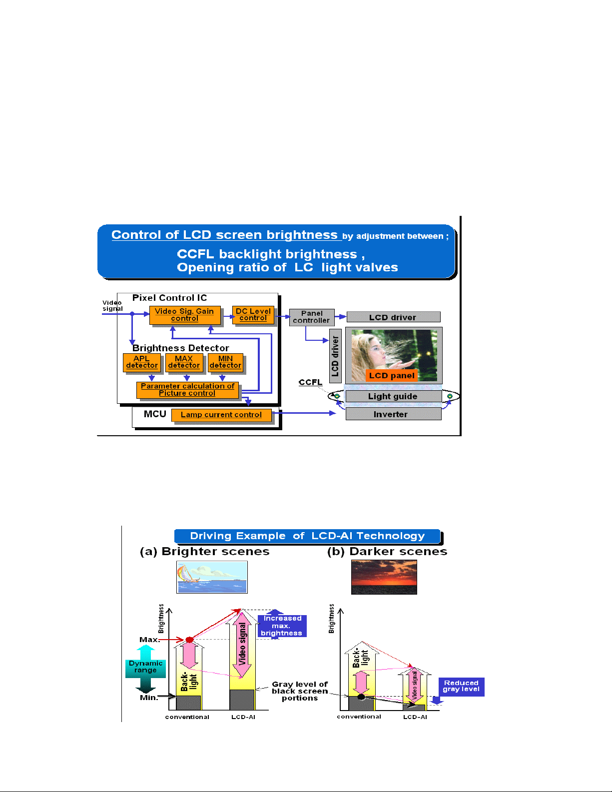
Features
LCD Technology
The LCD AI (Artificial Intelligence) technology incorporated within this model is very
similar to that covered in previous LCD models. The Pixel Control IC, in conjunction with
the Main Microcontroller IC, located on the DG Board, is responsible for controlling the
backlighting and the active matrix display addressing.
Backlight Brightness Control
Figure 1
Dynamically balancing the white light produced from the backlight produces a clearer
and crisper image.
Figure 2
2
Page 8
Dynamic Image Balancing
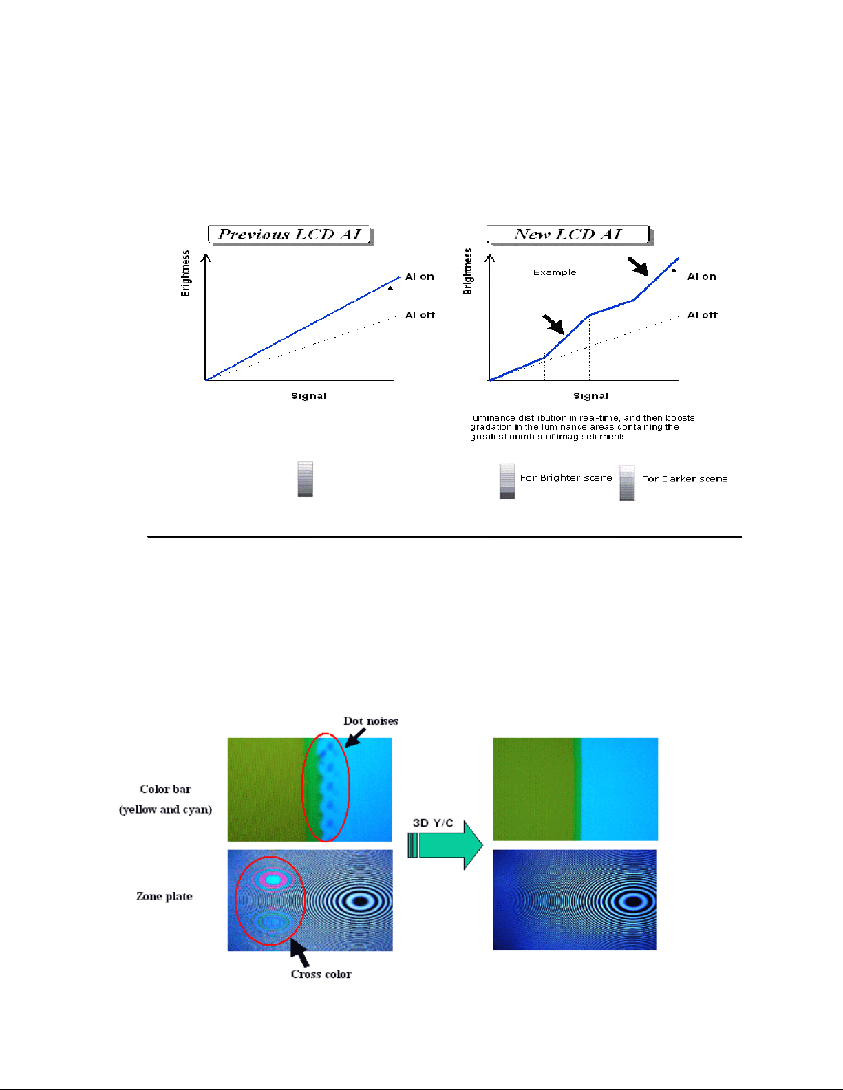
Enhancements have been made in the LCD AI technology as newer units evolve. This
is an example of the improvements made in the luminance distribution in real time.
Dynamic Image Enhancement
Figure 3
3D Y/C Separation
The luminance and chrominance of the composite video signals are separated using a
three dimensional Y/C separation circuit commonly known as a Comb Filter. Dot noises
or phenomena known as dot crawl and cross colors are reduced.
Figure 4
3
Page 9

LCD High Definition TV Model Differences
Differences between Models
The significant differences between models associated with the TC-22LR30 combo unit
(TC-26/32LX20 series) can be found in the following areas.
L
CD TV Section
The GC3 Global c
Microcontroller, the Video SW, and the Audio SW are same as that of the LCD TV
26/32LX20).
D
VD-RAM Section
The DVD Digital C.B
(DMR-E65). However, the software that resides in (IC6702) is different.
The equipment used for servicing the DMR-E65 is same as the one used
this model’s DVD-RAM Drive .The only difference is that the DVD Recorder (DMR) has
been downsized to a physically smaller drive.
C
ircuit Board A
The input and out
SW (IC3101).
The input and o
SW (IC3102).
The MTS/SAP
C
ircuit Board DG
The Main Micro con
incorporate communication with the DVD Recorder Circuit.
C
ircuit Board RD (Main DVD Bd.)
This Circuit Board was added to acc
ircuit Board M8 (DVD Digital Bd.)
C
This Circuit Board was added to accom
Microcontroller (IC6001) on this Board is identical to the one that resides
E65 Controller board and functions accordingly.
ircuit Board DV (HDMI Interface)
C
This Circuit Board was added to acco
(HDMI).
ircuit Board P and AP
C
The Primary (P) and Seco
the voltages required to power the DVD Recorder.
ore IC series that are used for the Video Signal processing, the
(TC-
.A. (Circuit Board M8) is the same as that of the DVD Recorder
for servicing
put signal lines for the DVD Recorder Circuit were added to the Video
utput signal lines for the DVD Recorder Circuit were added to the Audio
Audio Signal Process (IC3299) was added to record SAP to the DVD.
troller (IC1106) software was modified from the previous model to
ommodate DVD Recorder.
modate the DVD Recorder. The
mmodate the High Definition Multimedia Input
ndary Power Circuit Board (AP) were changed to incorporate
on the DMR-
4
Page 10
A
A
V
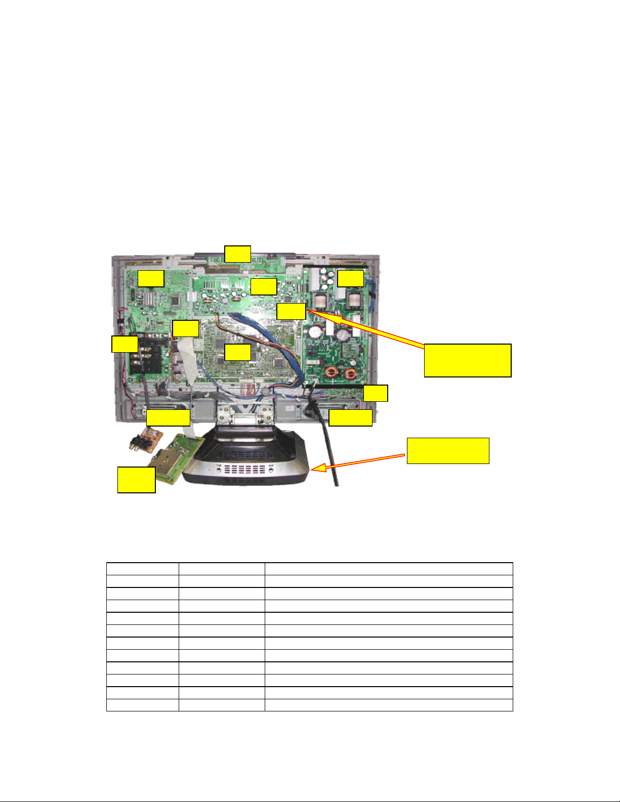
Circuit Board Layout
T
C-22LR30 Circui
t Boards
The TV portion of the combo unit is very
omprised of the following boards along with their associated part numbers as shown in
c
similar to that of the TC-26/32LX20 and is
this figure. Disassembly of this unit is much easier than the disassembly of the unit
covered in the previous online course because the stand or base doesn’t have to be
removed for removing the rear cover.
Rear op
K
H
L
D
en view TC-22LR30
DG
Spk LSpk R
P
DG Board is
located under
TA
Tune
Figure 5
Board Name Par
RFKZ0214 Extension Cable
DG
A
TA
L
V
P
AP
HA
DV
K
TV Portion Circuit Board Description
t Number Description
LSEP2163AE PCB Digital Core
LSEP2164B Input/Output Switching PCB
LSEP2191A Tuner PCB
LSEP2233A Digital Audio Jack PCB
LSEP2169B Front PCB
LSEP2189A AC-DC Power PCB
LSEP2232A DC-DC Power PCB
TNPA3162AB HDMI PCB
LSEP2170B Top Operation PCB
Table 1
DVD DMRE- 65
SD Card Reader
B LSEP2199A HDMI Audio Jack PC
5
Page 11
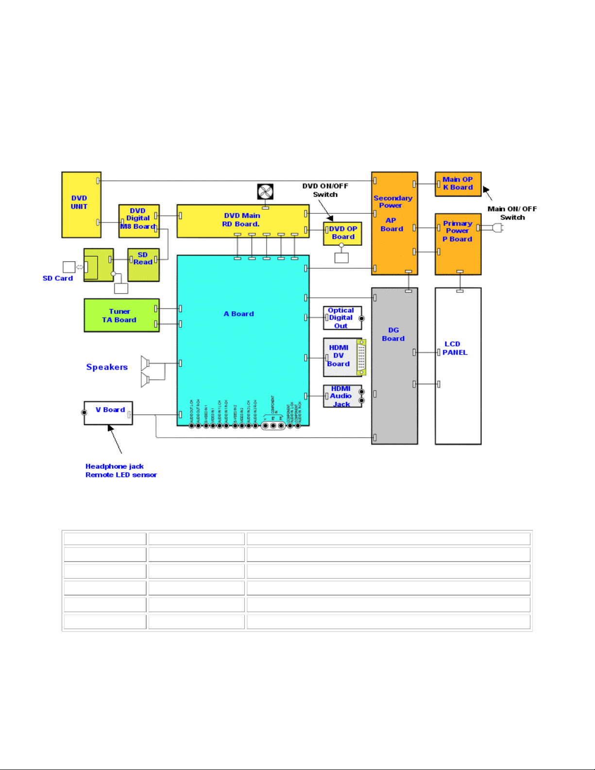
Circuit Board Interconnection
T tended to provide an overview of the interconnection o
his diagram is in f the various
circuit boards of the TC-22LR30 LCD Combo Unit.
Circuit Board Interconn
SR
ection
Board Name Part Num
RD
OP
SD
SR
M8
LSEP2171B PCB DVD MAIN
LSEP2175A DVD OPERATION PCB
LSEP2234A SD PCB
LSEP2235A SD JOINT PCB
RD-DKK005- DVD DIGITAL PCB
Figure 6
DVD Portion Circuit Board Description
ber Description
Table 2
6
Page 12

System Control Block
The control signals responsible for the overall operation and control of both units are
shown in this diagram along with their designated termination points.
Main Power switch signal is derived from the power on switch, which is loca ted on
the K board. The Main Micro (TV Microcontroller), located on the DG board, sees
this as a “key scan” input signal and issues a TV ON and AC_On to the control
circuitry within the Primary and secondary power supply.
DVD Power sw itch signal is derived from the DVD operation switch, located on the
DVD OP board. This signal is responsible for initiating the power on sequence for
the DVD operation. The Main Micro sees this as a “key scan” input signal.
Panel ON signal appears on pin 28 of the DG board connector DG2. This is
equivalent to an on/off switch for the LCD Panel.
Backlight ON /OFF (B/L On/Off) signal provides the enable for the DC to AC
backlight inverter power supply which is incorporated within the LCD Panel.
OSD Timing Compensator synchronizes the OSD with the incoming video.
System Shutdow n
The Main Micro on the DG board is responsible for monitoring the various shutdown
conditions. The Main Micro monitors the SOS and main voltage (Zero X Detect)
detection signals via the DG2 connector.
LED Functions
o The Time Warp Led indicates that the DVD is recording at twice the normal
record mode (operator’s choice)
o The SD LED indicates that the SD card is being accessed either for a read or
a write operation
o The DVD LED indicates that the DVD unit is being acces sed either for a read
or a write operation
TV Data In/Out are DVD control lines used for playback and record.
DVD Play switches the audio monitor output from all audio inputs to the DVD
Output.
Wake Up provides Serial data communication between the DVD Micro and Main
Micro.
Fan Control is accomplished through the use of a fan control circuit located on the
DVD main circuit board. A PWM output signal from sub processor IC 7501 controls
the speed of the fan, based on the internal ambient temperature of the unit
7
Page 13
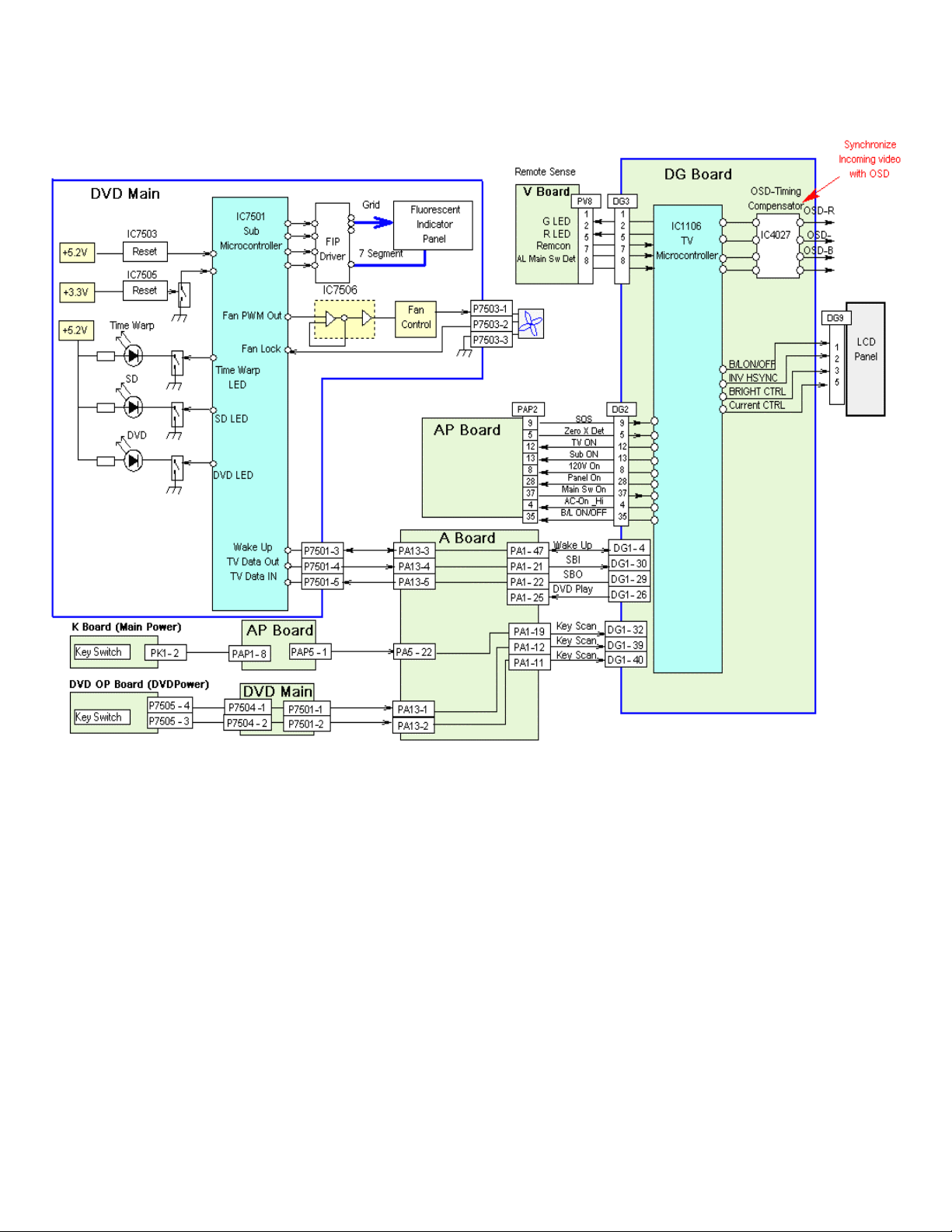
System Control Signals
Figure 7
8
Page 14
Circuit Board Description
A Board (TC-22LR30)
The A board serves as the main board and is comprised of the following:
The Video Switch IC3101 is responsible for selectively switching all video inputs
(Component, Composite, S-Video and HDMI). The selected input is fed to the
DG Board via the connector A1.
The Audio Switch (IC3102) selects the desired audio input for processing by the
Sound Control (IC2301). The MTS (IC3103) performs stereo separation of the
tuner’s multiplex signal and sends the output to the audio switch.
The TA tuner board on the TC-22LR30 provides the same functionality as the B
tuner board found on the TC26/32LX20. The output is connected to the A board
via connector PA7.
The HDMI interface, which resides on the DV board, processes and converts the
digital video and audio signals to analog and outputs them to the DG board via
the video switch.
A board TC22LR30
IC3101
IC3103
IC3102
Figure 8
9
Page 15
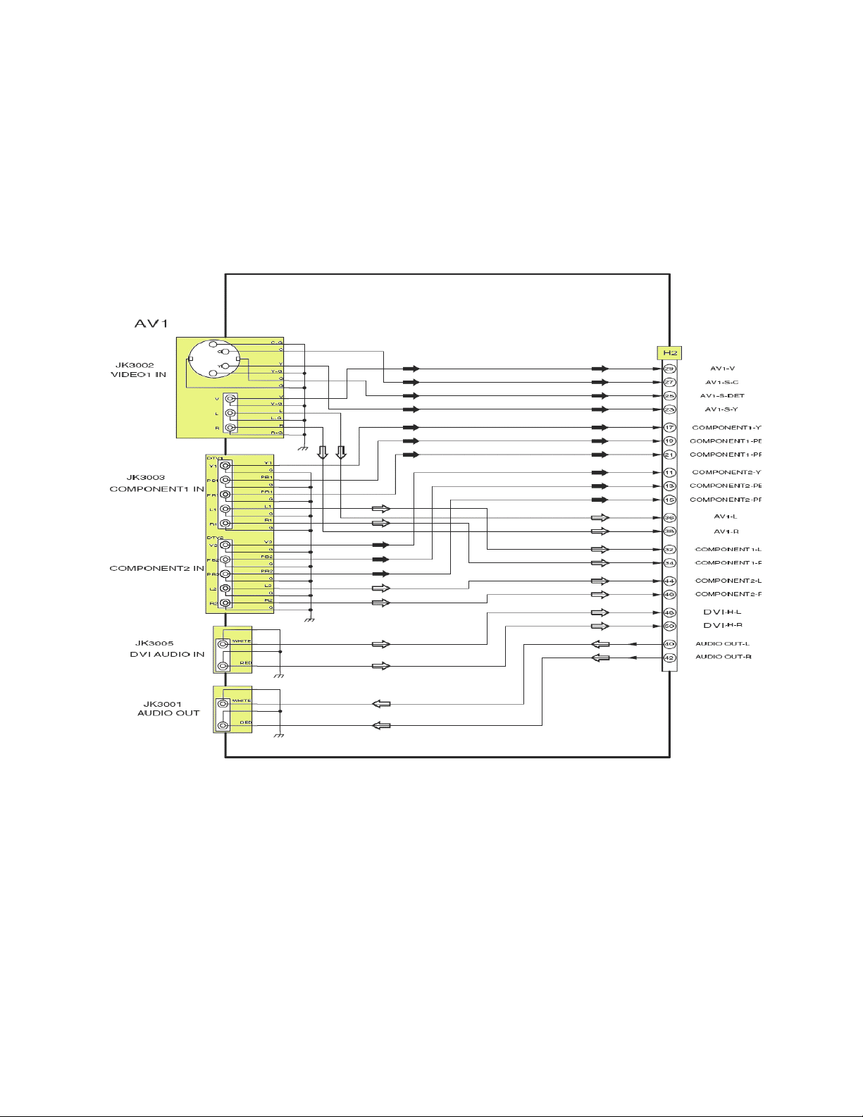
H Board (TC-26/32LX20)
The H Board on models TC-26/32LX20 is comprised of an S - Video and Composite
video input connection, two Component video inputs, a DVI audio input and an Audio
output connection. This board has been merged onto the A board of the TC-22LR30
Combo unit.
Figure 9
10
Page 16
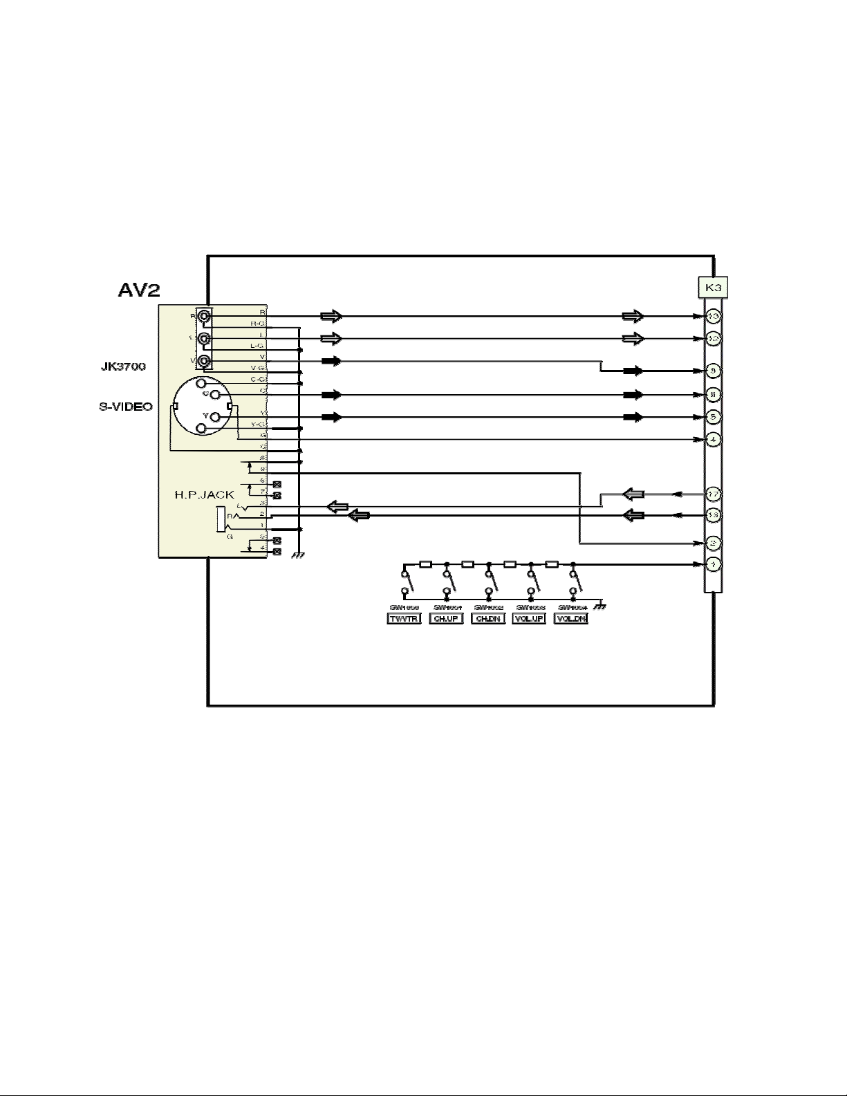
K board (TC-22LR30, TC-26/32LX20)
The K board contains the TV ON/Off, Volume, and Channel select buttons, and an
additional S-Video and Composite video input connector and headphone jack. It
connects to the A board via connector K3.
Figure 10
11
Page 17
A Board (TC-26/32LX20)
The A board for the TC-22LR30 Combo unit is very similar to that of the TC-26/32LX20
model. The H board has been merged onto this model’s A Board.
A Board TC26/32LX20
Figure 11
12
Page 18

Power Supply
Power Supply (TC-22LR30)
The power source for all models is comprised of a Primary and Secondary power
supply. The P Board is responsible for generating the primary source voltage used to
supply power to the secondary power supply, located on the AP board. It also supplies
the voltage that feeds the backlighting circuitry, which is incorporated on the LCD panel.
Newer models such as the TC-22LR30 use a 15 volts source that feeds this circuit (DC
to AC inverter). However, the TC-26/32LX20 and TC-32LH models use 120 volts as
input for the backlight circuitry of their LCD panel.
The AP Board is responsible for supplying all secondary voltages required for
operation. Modifications were made on the TC26/32LX20 models AP board to
accommodate the voltages required to power up the DVD RAM, which was basically
added to the TC-26/32LX20 to make it into a combo unit (TC-22LR30).
P Board TC-22LR30 Combo Model
Figure 12
13
Page 19

P Board - Primary Power
The Primary power supply is responsible for generating the following:
1. The standby power supply
2. The primary source voltage (14volts) for the secondary power supply.
3. Backlighting voltage (15 Volts) for the TC-22LR30
STANDBY POWER Circuit
The incoming AC voltage passes through the inrush current resistor R7001 and enters
the rectifier circuit consisting of D7015, D7022, D7023, and D7024 for conversion to
DC. The output is then applied to IC7005, a 7volt regulator. The 7volt output of the
regulator is sent to the AP board for conversion into 3.3V. This 3.3V is provided to the
DG board via pin 44 of the connector PAP2 to serve as standby voltage for the system
control circuit.
14V POWER SUPPLY
When a power up command is sent by the system control IC (Main Micro IC1106 on the
DG board), the AC_ON pin 47(connector PAP4 pin 13) sends a high to transistors
Q7002 and Q7003 to activate the power relay RL7001. AC passes through the relay
and enters the bridge rectifier consisting of D7005, D7007, D7008, and D7011.
The diodes convert the AC voltage into DC, which is then applied to pin 3 of IC7003 via
the transformer T7001. The voltage on pin 3 of this IC causes it to oscillate and output
a PWM pulse to drive the transformer T7001. As a result, energy is built and released
from the transformer.
The AC output at pin 11 and 14 of the transformer is rectified into 14 volts to serve as
the primary source for all other voltages. After the power supply starts running, the Run
Supply for IC7003 is supplied by diode D7033 connected to pin 8 of a secondary
winding of T7001. AC voltage from pin 8 of the transformer is also rectified by D7034
and applied to a switching control (regulator) circuit consisting of Q7005. Output of the
switching control IC is tied to pin 4 of IC7003 where it is monitored for over voltage
conditions. Voltage regulation is achieved via the 14V Error Detection circuit, which
consists of IC7006 and IC7008. The output of IC7006 is connected to pin 1 of IC7003,
the same input as the Run Supply.
15V POWER SUPPLY
This circuit generates +15Vdc used on the AP board. This voltage is also used to power
up the DC to AC converter for the backlight of the LCD Panel. The switched 14Volts
(sw+14V., which is generated when the unit is powered up), in conjunction with the
MAIN_ON_ACT (signal (H): approx.3.0V), allows Q7001 to turn on and activate the
Relay (RL7002). The rest of the operation is exactly the same as that of the 14 Volts
power supply.
14
Page 20

AP Board - Secondary Power
The Secondary power supply is responsible for producing the various voltages that are
required to power the DG board, the A board, the DVD unit and the LCD Panel VCC.
These voltages appear on connectors PAP2, PAP5 and PAP6.
• The 15V supplied from the P Board Connector PAP4 is converted to the
MAIN 12V, which supplies this voltage to the Audio AMP Circuitry located on
the A board.
• When a MAIN_ON signal (3.3V) from Pin 69 of Microcontroller (IC1106) is
issued to this board to turn off the Main power (MAIN 12V, 9V, 3.3V, 2.5V),
the MAIN_ON signal is converted to MAIN_ON_ACT to turn off Regulators
(IC801, IC806, Q801, Q803) which in turn terminates the Main power.
During normal operation the MAIN_ON_ACT signal (L) provides an enable to regulators
IC801, IC806, Q801, and Q803, which provides for the appropriate output of the Main
power.
AP Board Secondary Power Supply TC - 22LR30
Figure 13
15
Page 21

Tuner / FIP Power Supply (AP Board)
The circuit below, located on the AP board, is the power source for the NTSC tuner and
the FIP. At power up, the 14Vdc created on the P board is applied to the collector of
Q808 via pin 4 of the transformer T802. Instantaneously, The SUB_ON output of the
microprocessor, converted into SUB_ACT, outputs a Low to the base of Q809 to turn it
off. As a result, the transistor Q808 turns on via the startup resistor R815. Current flow
through Q808 and the primary of the transformer causes a magnetic buildup in the
transformer. When the transistor reaches saturation and current stops to flow, the
output current at the other windings of the transformer is rectified into DC voltages that
are used by the tuner and the FIP. To restart the operation of the circuit, feedback
current is provided to Q808 via the capacitor C823 and resistor R820. Over-voltage
protection is provided when the –30Vdc of the FIP circuit exceeds the reverse
breakdown voltage of zener diode D811.
30-Volt Tuner Power Supply Circuit
Figure 14
16
Page 22

Over Current Protection Shutdown Circuits
There are several protection (shutdown) circuits that monitor the voltage sources for
over voltage and over current conditions. They prevent the occurrence of catastrophic
failures by shutting down the unit. The circuit below is used to prevent catastrophic
failures if the Sub_5V, Sub_9V, Main_9V, or DR_12V becomes shorted. These are
voltage loss detection circuits that have the same method of operation. Let us analyze
the main 9V source as an example.
The circuit consists of a diode whose cathode is connected to a positive B+ source.
Under normal conditions, the diode is reverse biased, which keeps the base of Q832
high. However, if there is a short or excessive load on the Main 9V line that is being
monitored, the diode conducts, creating a current path for the base bias of Q832. The
transistor turns on and allows 3.3V to output at the collector. This voltage is then
provided to the base of transistor Q829 via the diode D874, forcing its collector to go
low. This low enters the SOS input of the MPU via pin 42 of the connector PAP2/DG2.
The MPU reacts by having AC ON (H) go Low. This, as you may recall, is supplied to
the SUB POWER CIRCUIT of the P board to shut off the SUB Power (14V) and the
MAIN Power (15V) voltage sources.
SOS Shutdown
Figure 15
17
Page 23

14-Volt Power Down Detect Circuit
he Zero X Detect circuit monitors the presence of the 14 volts source of the main
T
power supply (P board) and the Sub_5V of the AP board. Under normal operation,
pin
5 of the connector DG2 supplies a High to pin 61 of the MPU, IC1106. If, for any reason
the Sub_5V or 14 Volts lines drop or disappear, pin 5 of the connector DG2 becomes
low level to trigger a complete shut down of the unit
,
Figure 16
18
Page 24

Over Voltage Protection _ AC Shutdown Latch Circuit
This protection circuit is responsible for forcing the AC _On voltage to a low if any of
these protected voltages mentioned in the next paragraph become excessive. The AC
_On voltage is used to activate the relay RL7001, which is used to power up the unit.
AC Shutdown Latch Circuit
Figure 17
ransistor Q822 monitors the Sub_+3.3V, Sub_9V, Main_11.2V, DVD_5.9V, and
T
DVD_1.8V; Drive 12V, Sub_5V, and Sub_9V lines. If any of these supply lines incr
in voltage, transistor Q822 goes into conduction causing its collector to go low. As a
result, Q823 conducts causing the AC _On voltage to drop. Transistor Q822 and Q82
form a latch that keeps the unit from being turned back on until it is unplugged from the
AC outlet and plugged in again.
ease
3
19
Page 25

Power Supply (TC-26/32LX20)
The power source for all models is comprised of a Primary and Secondary power
supply. The P Board is responsible for generating the primary source voltage used to
supply power to the secondary power supply, located on the AP board. It also supplies
the voltage that feeds the backlighting circuitry, which is incorporated on the LCD panel.
Newer models such as the TC-22LR30 use a 15volt source that feeds this circuit (DC to
AC inverter). However, the TC-26/32LX20 and TC-32LH models use 120 volts as input
to this circuit.
P board (TC-32LH, TC-26/32LX20) - Primary Power
The Primary power supply is responsible for generating the following:
The primary source voltage (24 volts) for the secondary power supply
The 7-volt standby voltage for the system control circuit
Backlighting voltage 120 Volts for the TC-32LH, TC-26/32LX20
P board_ Primary and Standby Voltage Source TC-32LH, TC-26/32LX20
D7017
Figure 18
20
Page 26

Standby Power Supply
The standby power supply provides the necessary DC voltage to the system control
Microprocessor, the Reset circuit and the EEPROM. A.C. voltage is supplied to the Full
Wave rectifier (D7025, D7026, D7031, D7030), through the Line Filter and Transformer
T7004. The 7volts standby voltage produced by the rectifier is present as long as the
unit is plugged in.
The 7volts output passes through the AP board and enters the DG board where it is
regulated to 3.3V and fed to the system control circuit. Although the unit is plugged into
the wall outlet, the main power switch located on the front face of the unit must be in the
ON position for the unit to enter and remain in the standby mode.
Primary Power Supply
When the system control circuit obtains a power up command from the operator, the
AC_ON pin of the MPU, IC1105, outputs a high to the relay control circuits Q7011,
Q7012, Q7015 & Q7016 to activate the relay RL7001. The AC voltage enters D7002 for
rectification into 24 volts DC where it activates the relay control circuits Q7013 and
Q7014 to activate relay RL7002. The DC level is then boosted to 380Vdc by the Power
Factor Control (PFC) circuit, IC7002. The power factor control circuit is made up of an
oscillator used to control the charge and discharge time of the transformer T7001. Start
up voltage for the circuit is obtained at the output of the D7002.
As the PWM pulses are output from IC7002, the transistors Q7003 and Q7004 are
switched ON/OFF to allow the charge and discharge of the transformer T7001. The
charge of T7001 is added to the rectified voltage of D7002 to create 380V. IC7002 also
outputs a PWM output that turns the transistor Q7007 on and off to control the charge
and discharge time of the transformer T secondary output of the transformer
is rectified to 24Vdc and supplies the AP board. The diode D7017 rectifies the AC
output of on Run
Supply for IC7002. The 24Vdc
gulation. The output of this power supply is also monitored for excessive voltage by
re
D7022 and IC7004. If the output rises to 30 volts or more, the zener diode D7022 goe
into conduction, causing the photo-coupler to conduct and stop the operation of IC7002.
e of the secondary windings of the transformer T7002 to serve as
output is monitored via IC7008 and IC7003 for voltage
7002. The
s
21
Page 27

Power Supply Operation (TC-32LH, TC-26/32LX20)
D7011
T7004
Figure 19
Power On Operation of the DC-to- DC converter
The P board contains the drive voltage oscillator circuit that develops the 121 volts
needed to drive the LCD backlight. Operation begins with the discharge of transformer
T7002. The diode D7018 rectifies the AC voltage from the secondary of the transformer.
Approximately 30.1Vdc from the diode passes through the photo-coupler IC7005 and
22
Page 28

enters pin 6 of IC7001 to begin the oscillation. The pulses that ar
e output at pin 1 of the
oscillator enter the transformer T7004, causing it to build a magnetic field. The output of
the transformer is rectified into 121Vdc and rovided to the LCD panel via the connector
p
P4. When the rectified output of the transformer reaches 90Vdc, the diodes D7043,
D7044, D7045, and D7046 go into conduction, turning on transistor Q7010 and thereby,
turning off IC7005. This eliminates the start up voltage of IC7001. The oscillator
continues to operate using the run supply created by a secondary of the transformer
T7004 and the diode D7014. See Figure 19.
Power Off Operation of the DC-to-DC converter
When the unit is turned off, the 120V_Stop command is provided at pin 2 of the
connector P1/AP10. This causes the transistors Q7008 and Q7009 to turn on and stop
the conduction of IC7005 and IC7006. See Figure 20.
The 120V_Stop line is designed to stop the operation of the backlight DC-to-DC
converter if there is a drop or an increase in the 24 volts supply to the AP board. Pin 2
of the connector P1/AP10 inputs a High to the P board causing the transistors Q7008
and Q7009 to turn on. This causes IC7006 to immediately turn on and short pins 6 and
7 of IC7001. This action stops the oscillation of IC7001. To keep the oscillation of the IC
from starting again, the DC supply is grounded through Q7008.
Protection of the DC-to-DC converter
Over-current protection of the circuit is provided at pin 7 of the IC7001 from the emitter
output of Q7018.
Over-voltage protection of the primary is provided via the diode D7054. If the rectified
voltage of D7018 exceeds the operating voltage of IC7001, the diode D7054 conducts
and applies DC to the base of Q7019. The transistor Q7019 turns on and causes Q7018
to turn off, effectively removing the feedback voltage to pin 7 of IC7001. This action
stops the operation of the oscillator.
23
Page 29

This is a simplified overview of the activity that occurs within the primary power supply
section when the unit is turned on.
Figure 20
24
Page 30

A
P Board - Secondary Power Supply
The 14 volts derived from the primary power source on the P board enters the AP
power board, on the designated connector. The various voltages derived are used to
power the DG board, the Audio Control circuitry and the Tuner. If the 24volts shuts
down, a 120volt stop signal is generated which causes the unit to shutdown.
AP Board TC-26/32LX20
Figure 22
25
Page 31

Secondary Voltages
The Main 3.3V, 2.5V and Sub 5V, are used to provide power to the DG board. IC80
2
provides a regulated 9 volts to IC808, which serves as the voltage source for the tune
Its output is 30 volts. The Main 9,10 and 12.4 volts supply the secondary source vol
tage
to the rest of the unit.
Secondary Voltages
24V
r.
Figure 23
26
Page 32

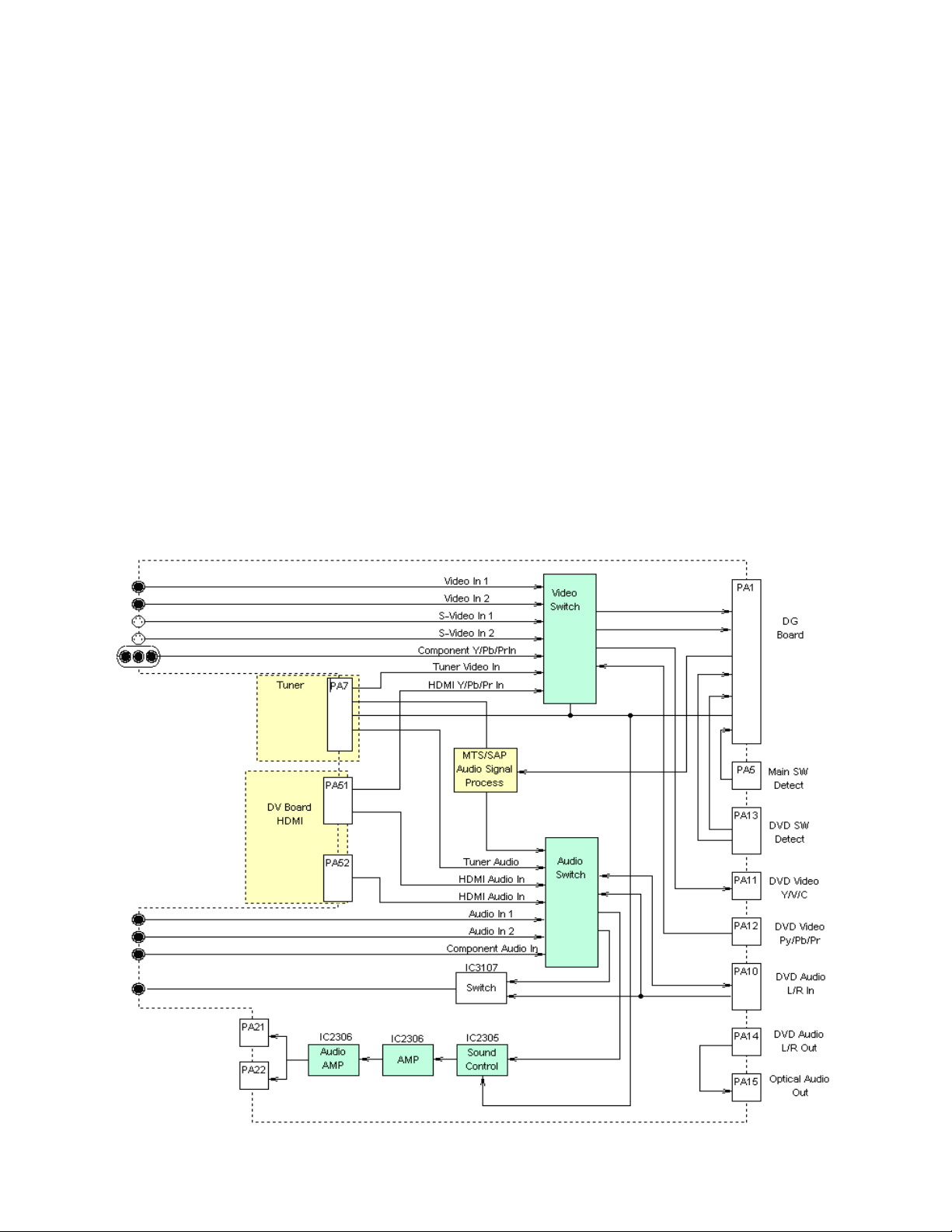
Video Circuit Explanation
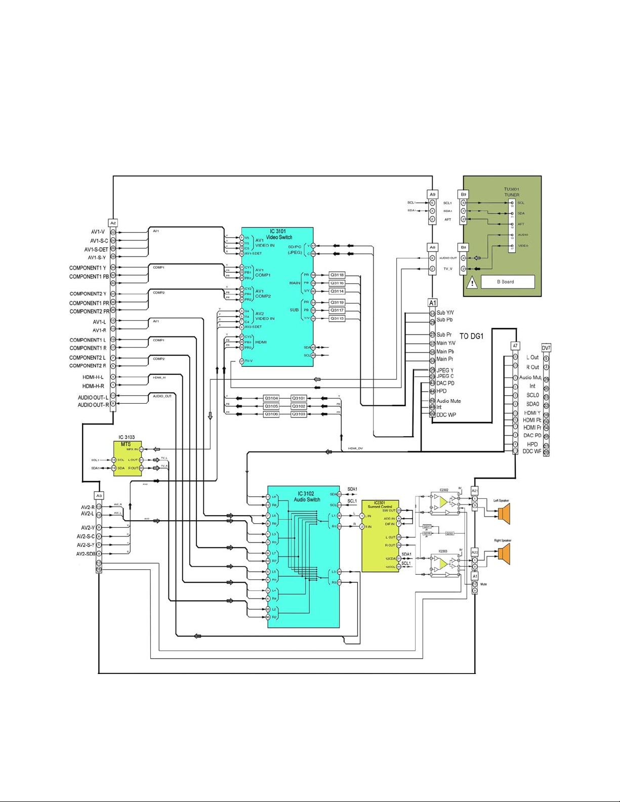
A Board
he A board serves as the entry point for all video signals that will be selectively
T
processed by the DG board via Video Switch IC3101. The main microcontroller, which
resides on the DG Board, is responsible for the selection of the designated video input
through the use of the I2Bus select lines. Two composite, two S–Video inputs, a
Component, a single Tuner, an HDMI video, and a DVD video interface are selectively
switched for video processing on the DG board. Connectors PA1 and DG1 serve as the
signal access point.
Video read from the SD Card is processed by the DVD main unit (M8 and RD)
where it enters the Video switch as DVD component Y/Pb/Pr video. Its output
appears on connector PA1 as Main Y/Pb/Pr video where it enters the DG board
on connector DG1 pins #37, 35, and 33.
HDMI video from the DV board enters the video switch as HDMI Y/Pb/Pr and is
also switched to the Main Y/Pb/Pr video input on the A Board
The NTSC tuner inputs, and the S-video and composite inputs to the video
switch appear on DG1 pin 37.
Video Path.
Figure 24
27
Page 33

DG Board
The DG Board is responsible for processing all incoming video signals from the A
board. The Vid
quired to drire
GC3FM (IC4011) and Video Signaling Processing IC4002.
The Microcontroller, IC1106 (DG board), controls the incoming video signals on the
Combo Unit (TC22LR30) in the same way as it does on the TC-26/32LX20.The
difference, however, is the addition of a serial data line between IC1106 and the
Microcontroller IC7501, located on the DVD RD board.
The main Microcontro
Decodes the remote control input code
Provides Channel selection
Global Core control
Sound volume control
to the DVD recorder is processed by
OSD Display. The OSD data that pertains
Microcontroller (IC6001), which resides on the M8 board. The TV OSD is mixed
with the DVD OSD on this board and is fed to the Video Switch
is located on the A Board.
eo input signals are processed and converted into the LCD format
ve the LCD Panel. This is accomplished by the main global core IC
ller IC1106 is responsible for the following:
(IC3101), which
Board Layo
DG ut
Figure 25
28
Page 34

Video Signal Processing
All NTSC video signals are converted to digital data by the analog to digital (A/D)
converter circuit located inside the Global Core IC, IC4011. The comb filter in IC40
converts the composite video signal of the main picture to Y and C separated vide
data. The S-Video signal, which is already Y/C separated, by
passes the comb filter. The
Chroma information is then applied to the Chroma Demodulator circuit that separates
the color signal into PB and PR data.
The Component inputs, which are already Y/C, separated; are converted to digita
bypass the comb filter section of this IC4011. The 480p
and 1080i ATSC Video signals
simply pass through the IC (which IC) and are output to the main global core IC,
IC4011.
Interlace to progressive (I/P) conversion for the 480i video format is accomplished via
the Video Signaling Processing IC, IC4010, and SDRAM IC4018 which serves as a
temporary buffer during the interlaced to pr
Sig
nal Processing IC is responsible for Pixel conversion, White Balance, Aspect Ratio
I/P con
version, Image resizing and LCD Panel control.
Video Signal Flow
ogressive conversion process. The Video
11
o
l and
Figure 26
29
Page 35

Low Voltage Differential Signaling
The method used to transfer the video information from the Main circuit board to th
LCD drive circuit is called Low Voltage Differential Signaling (LVDS). LVDS devices
typically consume less power than other signaling systems such as TTL. LVDS devic
use a constant current driver. Therefore, power consumption is independent of
frequency. The LVDS interface voltage is much less than TTL, approximately 2V. The
voltage swing is typically 350mV with a
VDS technology distribute signals with low-jitter, while creating little noise.
L
In this application, three 8-bit streams of data are converted from parallel to serial and
interleaved. The interleave process makes the data less susceptible to noise. The
to-peak v
onsumption and the generated noise from data transmission. Another benefit of the
c
LVDS standard is minimal concern for cable length. The data rates for LVDS are 110
Mbps for a 1-meter distance, dropping to 90 Mbps over a 10-meter distance.
oltage level is reduced as well. The lower voltage level reduces the power
n offset of 1.25V. Integrated circuits based on
e
peak-
es
Figure 27
30
Page 36

Figure 28
31
Page 37

HDMI Signal Path
The HDMI (High Definition Multimedia Interface) resides on the DV board as depicted in
Figure 29 and serves as an input port designed to receive digital video and audio from a
set-top box, a DVD player or other digital devices. IC5003 converts the digital video to
parallel analog RGB video. The outgoing audio is converted to analog via IC5006 and
IC5007. EEPROM IC5001 serves as the content protection circuit and monitors the
HDMI signal for copyright protection. IC5005 selects between HDMI and DVI audio.
Note: If the external device has DVI output only, use a DVI to HDMI adaptor cable in
order to connect to the HDMI jack to the DV HDMI connector. Also, connect the Audio
Out signal from the external device (set top box or DVD player) to the Audio In jacks. An
HDMI to DVI conversion cable (TY-SCH03DH) is available at the Panasonic parts
department.
DV Board HDMI Interface
Figure 29
32
Page 38

Self-Check Function for TV Section
The self-check feature is designed to check if a particular component is functioning and
it does not actually diagnose the problem .For example “Tuner Check OK” doesn’t’
necessarily mean that it is OK. It pings or selectively addresses that particular device
via the I2 Bus to determine if it exists. The same holds true for the Global Core IC’s, the
MTS, the Sound circuit, and the Audio/Video switches. However, it should be noted that
the displayed results could be misleading by indicating that it is OK.
The troubleshooting section of this document is intended to provide the necessary
guidance and assistance in the fault isolation of a particular problem and will serve as a
diagnostic tool for troubleshooting.
Self-Check Access
To access the self check mode:
Press the VOLUME-Down Button on the unit and SLEEP button on the remote at the
same time. To exit press any key.
Self-Check Display
Figure 30
33
Page 39

Servicing the TV Portion
Service Adjustment Mode for TV
Purpose of Adjustment mode
Adjustment mode provides the technician with the ability to perform standard video an
audio adjustments.
ow to enter the Adjustment mode
H
While the unit is powered on, hold down the
“Volume Down” button on the unit while pressing
the “Display” button on the remote three times
(within 2 seconds).
The service adjustment mode me
on screen as shown on the right.
Service mode is broken down into two
categories, Main Items, which are all displayed
on the menu screen and Sub Items. Refer to the
chart on page 35 to see the relationship between
the Sub Items and the Main Items.
How to navigate the Adjustment mode
Use the number buttons “1” and “2” on the
remote control to change the Main Item. The
number “1” button will cycle from the MAIN
option down to the DVD option. The number “2”
button will cycle in reverse direction.
Use the number buttons “3” and “4” on the
remote control to cycle through the Sub Items
until the proper adjustment is reached.
Adjustment of the Sub Item is made using the
“Volume” buttons on the remote control.
Data changes are saved automatically when you switch Sub or Main Items, or if you exit
the service mode.
Note: When the DVD adjustments are accessed, the unit switches to the DVD mode.
The software version of the DVD Player can be displayed here.
nu will appear
d
34
Page 40

How to exit Adjustment mode
Switch off the “Power” button on the main unit or press the “Power” button on the
remote control.
Warning: If you are making adjustments in the service mode, keep a record of the data
value before making the adjustment.
Service Adjustment Mode Chart
Main Item Sub Item Remarks Sample Data
MAIN
SU
B
YGAIN Video level (RF, Video, Component,
D)
DV
B-Y Video level (RF, Video, Component, 96
DVD)
R-Y Video level (RF, Video, Component,
DVD)
ANGL (R-Y demodulation axis) 20
BYGN (B-Y gain) A6
BRIGHT (Sub-bright) 7B
COLOR (Sub-color) 54
TINT (Sub-tint) 6A
BACK-L (Sub-backlight) C0
R-CUT 3C
G-CUT 3C
7D
52
GAMMA
DVD
B-CUT 3C
RED Panel Luminance (Color Temperature) AD
GREEN Panel Luminance (Color Temperature) AD
BLUE Panel Luminance (Color Temperature) AD
OPTOO (TV) 00 OPT
OPTDO (DVD) 00
CHROMA 13
CB GAIN 1C
CR GAIN 01
VOLMAX F0
Table 3
35
Page 41

Servicing the DVD
Service Tools
his is a list of the service equipment thatT
portion of the LCD TV Combo
DVD Test Disc DVDT-S01 and DVDT-S15 (Supplied from SPC.)
Extension Ca
ble REKZ0214 (Supplied from SPC)
Shakanabi Software: Not supplied as service parts. (This software is used for the
repair of Circuit Board M8.)
Data change CD-R: Not supplied as se
repair of Circuit Board M8.)
M8 Circuit Board R
epair
1. Change what is referred to as the model setting data for the software that resides
in IC6702. This converts TC-22LR30 (D
ease in troubleshooting. Th
is is accomplished through the use of the Shakanabi
Software.
will be required for the repair of the DVD
rvice parts. (This CD-R is used for the
VD portion) to that of a DMR-E65 for
2. Repair Circuit Board M8 as you would rep
DMR-E65 DVD Recorder. Upon completion
setting data back to that of the TC
-22LR30.
Use the Data change CD-R to accomp
air the Digital C.B.A. that resides in the
of repairs, change (return) the model
lish this task!
se the Extension Cable (RFKZ0214) between the M8-Board and the RD-Board.
U
Extension Cable (RFKZ0214) has A/V Out
Output signals can be switched from the M8
When checking the M8-Board, turn the switch
When checking the RD-Board, turn the switc
put Signal switches.
-Board side or the RD-Board side.
es to the M8-Board side.
hes to the RD-Board side.
xtension Cable
E
Figure 31
36
Page 42

Troubleshooting
This section is in
repair of the LCD TV combo or LH34 chassis type in general. These include the TC22LR30 and TC-26/32LX20 models. These are some of the screen display symptoms
and conditions that may arise as a res
uring operation or while entering Self Check mode.
d
tended to serve as an aid in the fault isolation, troubleshooting, and
ult of an error or a problem that may occur either
Symptom Display Chart
Table 4
37
Page 43

Shutdown Problems
If a problem occurs in either the unit or power supply a protection circuit is activated and
the unit shuts down. The Power indicator on the front of the unit will flash red severa
times indicating an error code. Error codes vary for different models and will be included
in t
his document.
LE
D Flashes Three Times
Yes
Is the Sub 9V
present on pins
9 &10 of
connector PAP5
of the AP
board?
Yes
Is the Drive
+12Volts present
on pin 4 of
connector PAP7 of
the AP board?
No
Is the Drive 5
Volts present on
pin 8 of Q804 or
TP842 of the AP
board?
END
No
Check regulator
IC805 on
The AP Board.
Check regulator
IC 809 on the
AP Board.
Check pin 2 of
regulator IC808 or
pins 6 and 8 of
connector PAP2 of
the AP Board.
l
38
Page 44

LED Flashes Once every 5
Check the Backlight supply vol ge from the P board. ta
TC22LR30 -15 volts P2 pin 9-15 Ground pins 1-7.
TC26/32LX20- 120 volts P4 pins 1-2. Ground Pins 4-7
LED Flashes Five Times
Check the Main 9Volts Regulator
LED Flashes Eight Times
Check the Sub 5 Volts regulator, IC808.
Unit shuts down and the Power on LED is off.
seconds
Q801 on the AP Board
Check the SOS Shutdown and over-voltage
protection circuits. Please reference power
supply section of this document. Use the
troubleshooting flowcharts for the Primary
and Secondary power supply checks.
SOS Shutdown Problem
If the unit keeps shutting dow
Shutdown line at pin 9 of connector DG2.
It should be at a high level. Anodes of D877, D878,
D880, D844 all should be high.
n, check the SOS
39
Page 45

The Unit Does Not Play Video from Disc .
Check to see if there is an Input
signal on the TV Screen.
OK
Check the power supply to the
DVD RAM Drive. Pin1 should be
5Volts, and Pin 4 12Volts o
connector PAP7 on the
Board.
OK
Check connector P7402 on the
RD Board. Chroma out Pin 18
Luminance out Pin 22: Pin 26
out pin 26
G/Y
B/PB ou
R/P
Check connector PA12 on the A.
board for video.
Pin 1: Y IN
Pin 3: C IN
Pin 5: PY IN
Pin 7: PB IN
Pin 9: PR IN
t Pin 34
R out Pin 30
OK
OK
Continued on next page
AP
n
NG
NG
NG
NG
There is problem in
TV circuit.
Perform a Secondary
Power supply Check.
The DVD M8 digital board
or D s
VD RAM Drive i
defective.
The DVD RD Board is most
likely defective. Check the
video interface IC3001 and
the surrounding circuitry.
40
Page 46

Continued from last page
Th
e
A board is defective.
Chec
k t
he video switch IC3101
and
the surrounding circuits.
Is there an output signal to the
Speaker terminals?
OK
Check the power supply to the
DVD RAM Drive. Pin1 5V
Pin 4 12V on connector PAP7
located on the AP board.
Check connector P7402 on the
RD board. Pin 58: R OUT
Pin 62 L OUT
Check the PA1
A. Pin 5: L IN. Pin 7: R IN
Circuit Bo
Check IC3102 and t
surrounding circuit.
0 on Circuit Board
ard A is defective.
he
and
OK
OK
OK
NG
NG
NG
NG
There is problem in
TV circuit.
Perform Primary Power
ply Check. Sup
Circuit Board M8 or DVD
RAM Drive is defective.
Check IC40
surr
ounding circuit on
the M8 board
01 and
41
Page 47

Does Not Record Video to Disc
Is video displayed on TV
screen?
OK
Check the power supply to DVDRAM
Drive (Pin 1 (5V) and Pin 4 (12V) of
connector PAP7 on AP Board.)
OK
Check for Chroma pin50, Video
pin 51 and Luminance pin52 of
IC3101 on the A board.
Check for Chro
Video on pin 3 an
on pin 5 on connector PA11 of
the A Board
ma on pin 1
d Luminance
NG
NG
NG
There is problem in
TV circuit.
Check the Primary Power
SupNGply circuit
Replace IC3101.
Check the signal line
between PA11 and IC3101.
OK
Check pins 1 and 2 on connector
n the RD board. P7402 o
OK
Check the Circuit Board M8 and
DVD-RAM Drive.
NG
Check IC3001 and
surrounding circuit on
Circuit Board RD.
42
Page 48

Does Not Recor Audio to Disc
Is there an output signal to the
Speaker terminals?
OK
Check the power supply to DVD
RAM Drive on the AP board.
Connector PAP7 Pin1 should
have 5V and Pin 4 should
have12V
OK
Check the Audio Switch IC3102
the A Board. Left channel out
pin27 and Right channel out pin28.
OK
.
on
on
NG
NG
NG
d
There is problem in
TV circuit.
Perform a
Primary Power Supply Check
Replace IC3102.
Check pin 1 DVD left in and pin
3 DVD right in on conne ctor
the A Board. PA10 on
OK
Check pin 48 and 50 for analog
audio in on connector P7402 on
the DVD RD board.
OK
Check the DVD M8 Digital bo
Drive.
ard
and the DVD-RAM
NG
NG
Check the signal line
between PA10 and IC3102.
Check the audio interface
IC4001 and surrounding
c
ircuitry on the DVD RD
Board.
43
Page 49

Primary Power Supply Check
Is th
e standby Voltage at
TP7015 7volts?
OK
NG
Check the Fuse F7001,
F7002 and IC7005.
Check the AC_ON signal
at TP7003 (0.7V).
OK
Check the voltage at
TP7013 (14V).
OK
Check the
120V_ON_ACT signal at
Pin 14 of PP4 It should be
approx. 0V.
NG
NG
NG
Check the Power on switch on
the K Board and the connection
between PK1 and PAP1.
OK
Confirm the PROTECT circuit on AP
Board is working. D824 should
measure 7V.
OK
Check the main controller IC1106
on the DG Board.
Repair the Sub power circuit on
the P board.
Check the Voltage at Pin 43 on
connector PAP2. (~ 0V)
G
OK
N
OK
Che
ck the voltage at
TP7016 (15V).
OK
The P board appears to be
working properly.
Confirm the DC-
DC
On/Off circuit on the
AP board is functioning
properly.
Repair the Main power circuit
NG
on the P board.
44
Confirm IC1106 on
Circuit Board DG.
Page 50

Secondary Power Supply Check
Confirm that the P board is good.
OK
Confirm the voltage at R870 and R873. (3V)
OK
1) Confirm the power control signals from IC1106.
MAIN_ON: (H) 2.4V, (L) 0V: Pin 39 of PAP2
SUB_ON
PANEL_O ) 2.4V, (L) 0V: Pin 23 of
PAP2
2 50
) Confirm the power control signals from IC7
P_ON_H: (H) 5V, (L) 0V Pin 15 of P
DR_P_ONH: (H) 5V, (L) 0V: Pin 16
PAP6
: (H) 2.4V, (L) 0V: Pin 38 of PAP2
N: (H
1.
AP6
of
OK
C regula
onfirm the power control signals to each
MAIN_ACT: (H) 2.4V, (L)
(L) 0V
SUB_ACT: (H) 2.4V,
PANEL_ACT: (H) 2.4V, (L) 0V
DR_P_ON T: (H) 2.4V, (L) 0V
P_ON_ACT: (H) 2.4V, (L) 0V
_AC
0V
tor.
NG
NG
NG
Check the R858, 860,
870, 871, 872, 859,
861,873, 874, 899, D841
and D842.
Check the IC1106 on
Circuit Board DG and
IC7501 on Circuit Board
RD.
C sistor.
heck the each Diode and Tran
MAIN_ACT: D830, D85
SUB_ACT: D832, D857
PANEL_ACT: D835, D858
DR_P_ON_ACT: D834, D860,
Q828
6
P_ON_ACT: D831, D859, Q827
OK
Confirm the output voltage from
each regulator IC.
OK
There is no problem in Circuit Board AP
NG
45
Replace the Regulator
IC.
Page 51

Appendix
klighting
Bac
Backlighting Brightne r Panasonic’s line of LCD TVs is accomplished through the
use of Cold Cathode Fluorescent tubes (CCFT), which is currently the light source of
choice, by a number of leading manufacturers.
Inverter Power Supply
Pulse width modulation is a very straightforward m f
the CCF tube(s). The inverter is turned on and off (using the input or an enable/disable
line) from the Microprocessor Unit (MPU) to contr cycle
is lengthened to increase the brightness and reduced to decrease the brightness. One
of the major advantages of pulse width modulation is the
“off” and full starting voltage is always applied to the tube(s) (assuming nominal input
voltage). Figure 5 is a simplified diagram of a pul DC to AC inverter.
ss fo
ethod for controlling the brightness o
ol the brightness. The “on” duty
tube is always fully “on” or fully
se width modulated
Figure 32
46
Page 52

High Voltage P
A CCF tube needs high voltage. The starting voltage is generally over 1,000 volts and
th tween 200 and 500 volts rms.
e operating voltage is generally be
Most CCFT DC to AC inverters are tuned switchers designed to produce a specific
voltage, frequency and output current when a designated tube is connected to the
output. The classic current-fed two-transistor inverter has a tuned resonating output,
tuned resonating input and inductive dc input which provides for good power transfer
and high operating efficiency.
ower Supply
Figure 33
The type of circuit depicted in Figure 6 inherently produces a pure sine-wave output, but
the voltage and current waveforms are both distorted when they are applied to a CCF
tube, which is a highly nonlinear device. The transition from the starting voltage to the
operating v ented by a small internal series output
pacitor, which serves as the balla
ca st, pro g imped er tube
current a en ignited.
oltage in this circuit is implem
vidin ance, and allowing prop
fter the tube has be
47
Page 53

Test and Measurement
This is a basic test
output voltage to th
w-capacitance (< 2.5 pf) scope probes. The oscilloscope should be connected
lo
differentially, with the probe grounds connected and floating as depicted in the diagram
Figure 7 indicates how an oscilloscope can be used for achieving these measurement
setup for measuring the output voltages of the inverter circuit. The
e tube can be measured with a dual-channel oscilloscope and two
.
s.
Figure 34
Channel A should be added to the inverse
waveform on the oscilloscope.
Output waveform
This is what the typical output current waveform should look like as viewed in the above
test arrangement.
of channel B to produce the complete
Figure 35
48
Page 54

Specifications
Combo Overall Specification
Picture
Response speed
Pixel
LCD AI (Adaptive
Brightness
Intensifier)
Discs Played Disc Type
22,26,32 inch Screen Size
450 cd/m2 Brightness
16 M sec.
W-XGA (1280 x 720)
New LCD AI
3D Y/C separation Other
DVD-RAM, DVD-R, DVDVideo, CD-Audio, Video CD,
DVD-AUDIO, CD-R/CD-RW
DVD-RAM, DVD-R Recordable Discs
SD Card
Still Picture Play
Table 5
JPEG, TIFF, DPOF
49
Page 55

V Portion
T
Table 6
50
50
Page 56

DVD Portion
The LCD Combo unit uses a DVD recorde
r, very similar to the DMR-E65
Table 7
51
 Loading...