

Page 1

Technical Guide
Colour Television
GP 31 Chassis
Circuit Explanations
Panasonic
Kuala Lumpur Malaysia Sdn. Bhd.
Panasonic AVC Networks
1
Page 2

Contents
Introduction 3
Location of Control & Circuit Boards 4
GP-31 Chassis Block Diagram 5
1. Tuning Circuit
1.1 Signal Processing 6
1.2 IF Control 6
2. Ultimate One Chip IC601
2.1 Features 8
2.2 IIC Bus 9
2.3 Memory IC 9
2.4 Reset Circuit 10
2.5 IC601 Pin Configuration 11
3. Video Circuit
3.1 Video Signal Processing 14
4. Audio Circuit
4.1 Audio Processor 17
4.1.1 Sound Processor 17
4.1.2 Audio Amplifier 17
5. Deflection Circuit
5.1 Horizontal Output Circuit 20
5.1.1 Horizontal Output Operation 21
5.2 Vertical Output Circuit 23
5.2.1 Vertical Output Operation 23
6. Colour Output
6.1 Colour Output Stage 24
7. Protection Circuit 25
8. Power Circuit
8.1 Start-up Circuit 29
8.2 Output Voltage Control 29
8.3 Regulation 30
8.4 Over Voltage Protection Circuit 30
8.5 Over Current Protection Circuit 31
8.6 Latch Circuit 31
8.7 Standby Operation 31
2
Page 3

! WARNING
This service information is designed for experienced repair technicians only and is not
designed for use by general public. It does not contain warnings or cautions to advise
non-technical individuals of potential dangers in attempting to service a product. Products
powered by electricity should be serviced or repaired only by experienced professional
technicians. Any attempt to service or repair the product or products dealt with in this
service information by anyone else could result in serious injury or death.
Introduction
We at Panasonic realise that the service engineer needs to understand the circuitry
inside the TV and for this need, we have produced this Technical Guide.
This Technical Guide contains information for GP 31 chassis and should be used
in conjunction with the relevant Service Manuals for this chassis.
As the Technical Guide for the GP 31 chassis covers such a wide range of models,
some differences may occur in circuit descriptions and component references.
3
Page 4
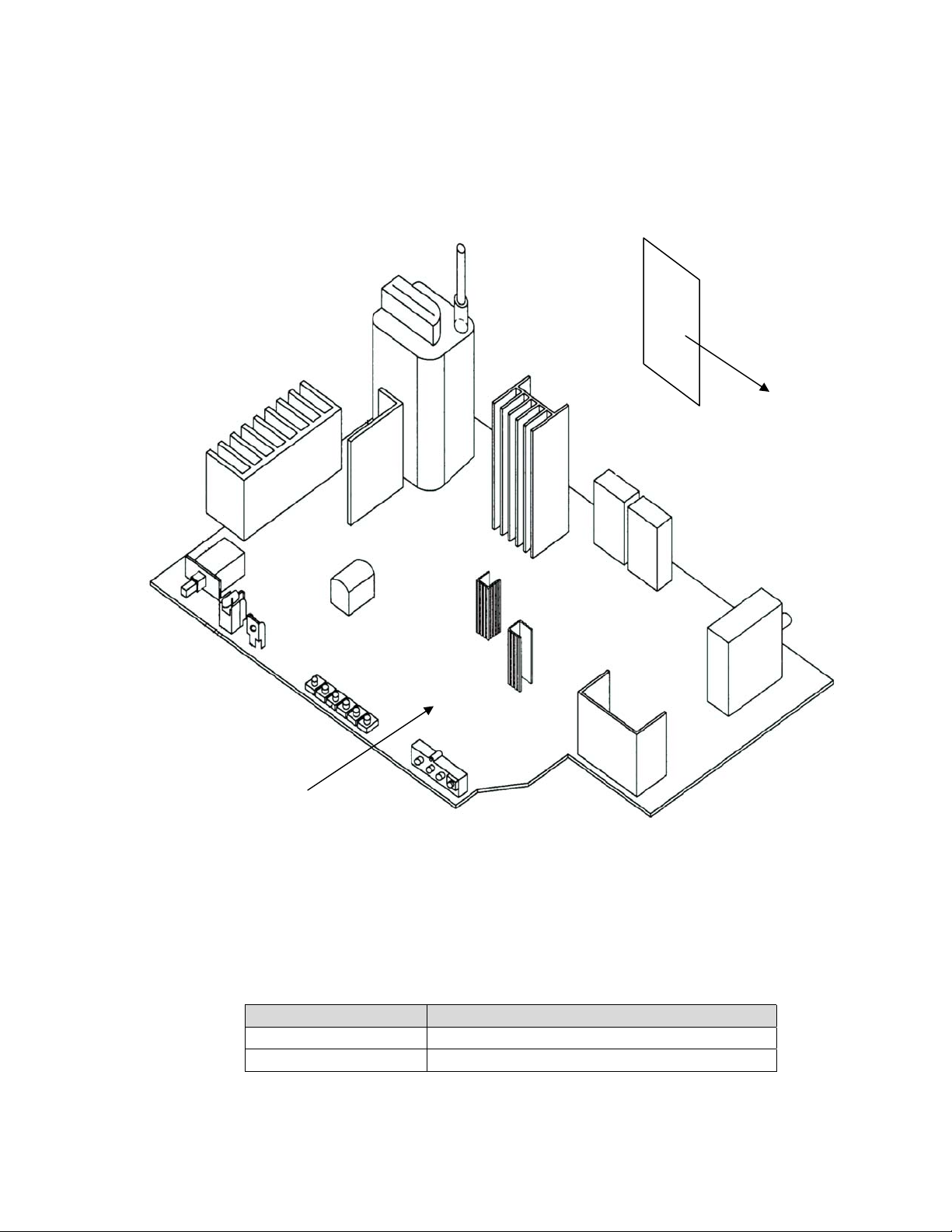
Location of Control & Circuit Boards
L-Board
A- Board
Board Name Function
A-Board Main Board
L-Board CRT Board
4
Page 5
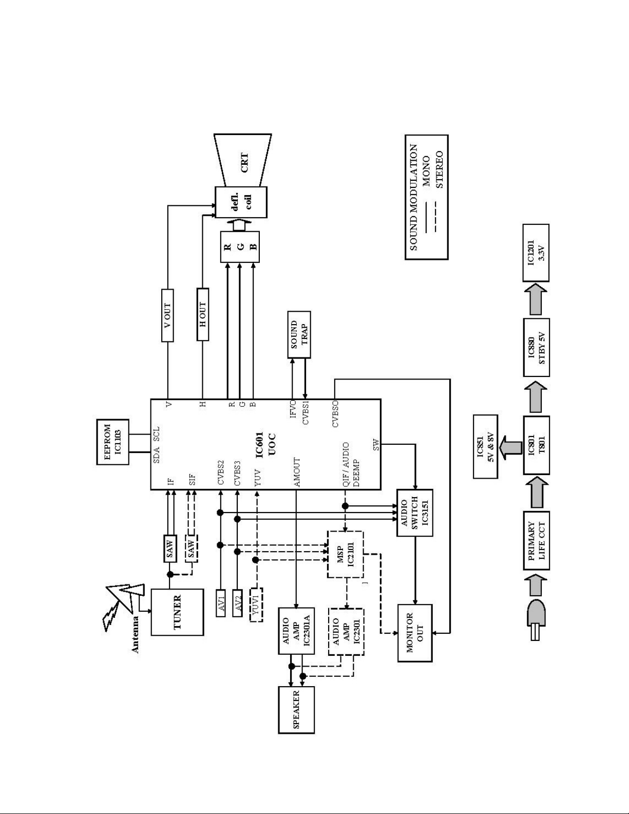
GP-31 Chassis Block Diagram
5
Page 6
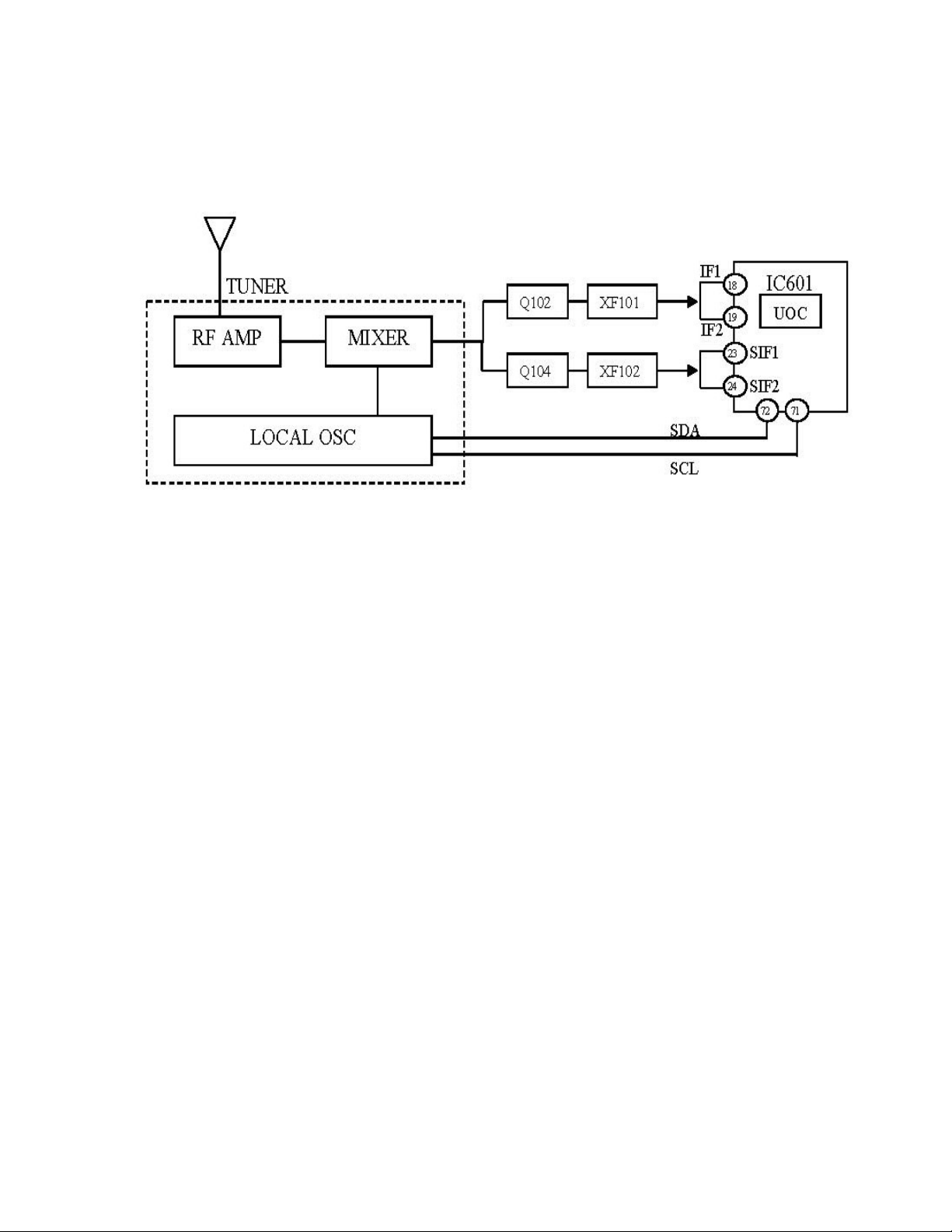
1. Tuning Circuit
Outline
The tuner is designed for reception of the conventional frequencies to date and the
intermediate special channel frequencies. The IF stage of the tuner contains the video and
audio demodulators which are designed for most widely used TV standards.
Fig 1.0
1.1 Signal Processing
1. The purpose of the tuner is to convert the VHF/ UHF TV broadcast signal (RF) into
intermediate frequency signal, IF (38.0MHz) [Fig 1.0].
2. The aerial intercepts the TV signal and amplified by the RF amplifier.
3. The local oscillator generates basic frequency to convert RF signal into IF signal
(intermediate signal) in the mixer.
4. Here the IF signals is output to UOC IC601 for video and sound processing.
1.2 IF Control
Control of internal Tuner-IF processing is performed by the UOC IC601, the
IC601 sending control information via I²C bus input via pin 71 (SCL) and 72 (SDA).
In addition to this, AGC control of the Tuner-IF stage is controlled by the UOC
via I²C. AFC information for Tuner-IF stage is fed back to the IC601 via control line
AGC (pin 22).
6
Page 7
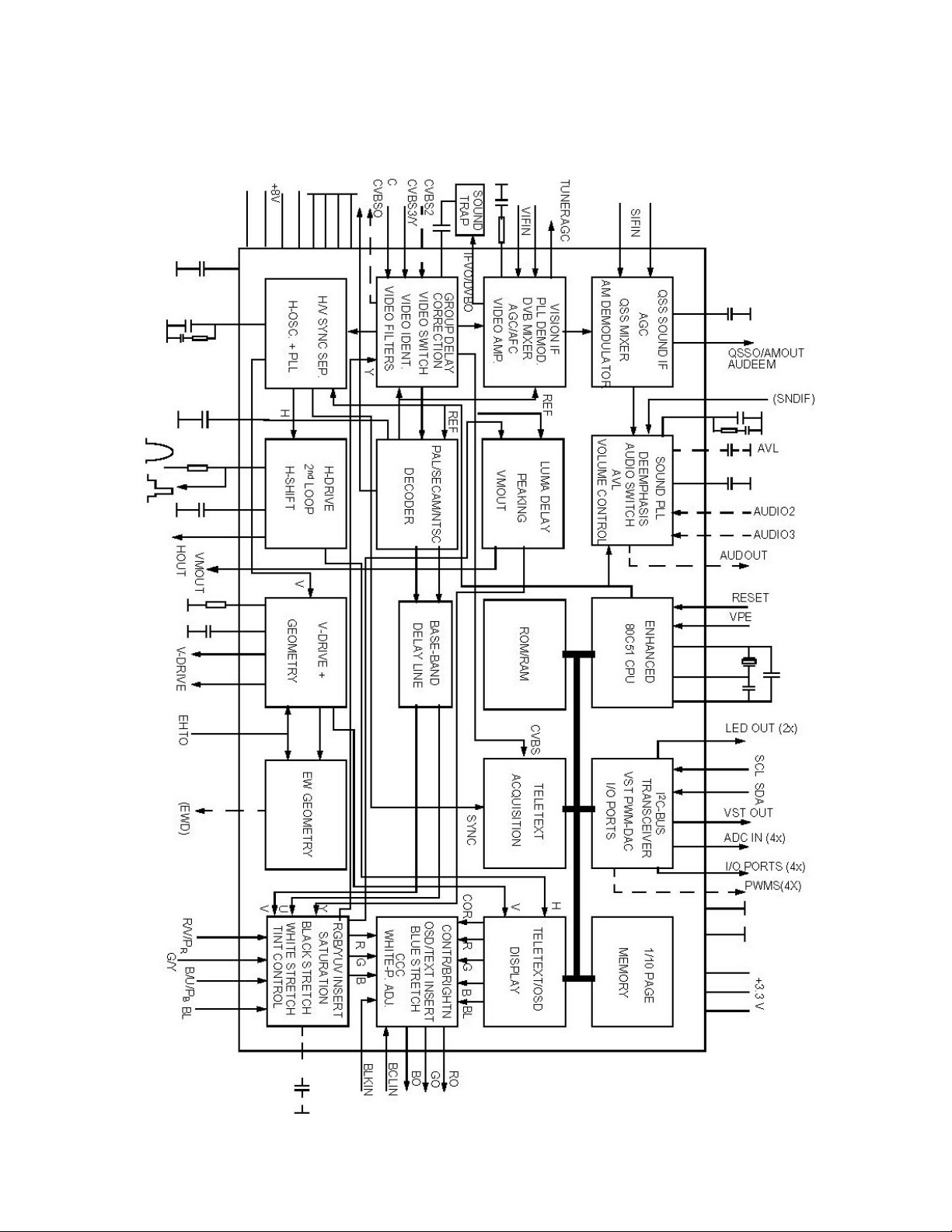
UOC IC601
7
Page 8

2. Ultimate One Chip IC601
Outline
The IC601 TDA959xN, also known as UOC, is a high-quality single chip TV
processors IC which allow the economic integration of features in all classes of singlescan TV sets. UOC combine the functions of a video processor together with a
microcontroller and teletext decoder.
The integrated microcontroller is supported by a powerful OSD generator with
integrated Teletext & Close Caption acquisition including on-chip page memory.
2.1 Features
a. TV Processor
• Multi-standard vision IF circuit
• Picture improvement features with peaking black stretching
• Multi-standard colour decoder with automatic search system
• Internal base-band delay line
• Horizontal and vertical geometry processing
• OSD/text gain reduction control
• White point and black level off-set adjustment
b. Micro-controller
• 80C51 micro-controller core standard instruction set and timing
• 1 µs machine cycle
• 128K-byte ROM
• 12K-byte RAM
• Data Back-up
Storage of tuning, switching, control and adjustment data to the memory
(IC1103) and reading out the data
• Switching and Control
Output of the control signal for picture and sound, etc., and switching signal
for TV/AV mode and so on
• Adjustment
Output of adjustment levels for UOC (IC601) through I²C bus.
c. Teletext Decoder
• Text memory for 1 or 10 pages
• Automatic detection of FASTEXT transmission
• Data Capture for US Closed Caption
8
Page 9
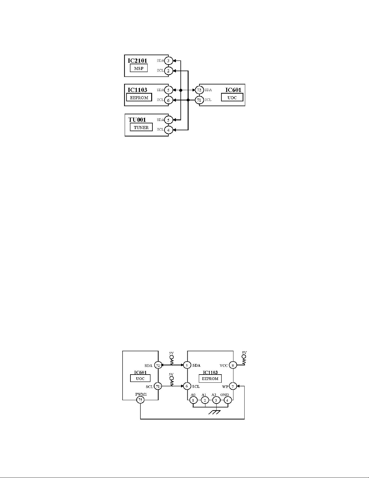
2.2 I²C bus
• The I²C bus is a two bus system consisting of a data line and a clock line.
• 5V is set for SDA / SCL. [Fig 2.0]
• Allow a large number of switching and control functions of GP-31 chassis.
The UOC IC601 generates bus signals which control the following hardware
configuration.
1. EEPROM IC1103
These memories are 1K-byte, non-volatile memories of microchips, and bit pattern of
1024 x 8 bits.
2. Tuner TU001
To select a desired channel signal from the several RF signal from TV stations and
convert the selected RF signal into a signal of an intermediate frequency (IF).
3. Sound Processor IC2101
The sound processor IC will cover the sound processing of all analog TV-Standards
worldwide, as well as the NICAM digital sound standards.
Fig 2.0
2.3 Memory IC
Fig 2.1
9
Page 10

The memory IC1103 receives the data listed below as supplied from the UOC
IC601 through I²C bus [Fig 2.1]. It is input or output whenever it is necessary. This
memory IC is a non-volatile type, which data is maintained permanently although the
power is cut off.
Last Memory Location
These memory locations will contain the following information that must be
stored inside even if power to the EEPROM is interrupted.
1. 100 channels of BT voltage and band (VL, VH, U) information.
2. 100 channels of AFC, SKIP, COLOR SYSTEM and SIF information.
3. Last position for each switching mode.
4. Volume data.
5. TV/ AV1/ AV2 mode.
6. Recall ON/ OFF.
7. Power and auto off timer setting.
8. Service mode setting.
9. The COLOUR, NTSC TINT, BRIGHT, CONTRAST and SHARPNESS DAC
data, and each SUB-DAC data, CUT-OFF, RGB-DRIVE etc.
10. PICTURE MENU & SOUND MENU.
11. AVL
Pin No. Name Function
1 A0 GROUND
2 A1 GROUND
3 A2 GROUND
4 GND GROUND
5 SDA Serial Data In/Out
6 SCL Serial Clock Input
7 WP Write Protect Input
8 VCC 5V
2.4 Reset circuit
1. Power on reset is generated internally to the UOC IC601; hence no external reset
is required. (The TV processor generates the master reset in the system, which in
turn will reset the micro-controller.)
2. During power ON operation, or during a momentary drop in the +B voltage,
insufficient voltage supply to UOC IC601 may occur. Thus, there is a possibility
that incorrect operation of the UOC occur.
3. In order to prevent incorrect operation, a resetting pulse is activated until the
voltage fed to the UOC is normalized.
4. When the power switch is turned on, if the VDD of the UOC is less than 3.3V
then UOC starts to reset.
5. UOC start to function again when VDD becomes more than 3.3V.
10
Page 11

2.5 IC601 Pin Configuration
Pin No. Name Function
1
2 AUTO/MAN
3
4
5
6
7
8
9
10
11
12
13
14
15
16
17
18
19
20
21
22
23
24
25
26
27
28
29
30
31
32
33
34
35
36
37
38
39
40
KEYSCAN Panel key
Geomagnetic controlling
H: Auto L: Manual
MSP RESET H: Normal
L: Reset (During power ON)
GND (D) Digital ground for µ-Controller core and periphery
AV/TV TV / AV search
H: AV / Auto Search L: TV
4.5V / OTHERS H: 4.5MHz L: Other / AV
VSSA Digital ground of TV-processor
SECPLL SECAM PLL decoupling
+8V 2nd supply voltage TV-processor
DECDIG Supply voltage decoupling of digital circuit of TV-
processor
PH2LF Phase-2 filter
PH1LF Phase-1 filter
GND3 Ground 3 for TV-processor
DECBG Bandgap decoupling
EWD East-West drive output
VDRB Vertical drive B output
VDRA Vertical drive A output
IFIN1 IF input 1
IFIN2 IF input 2
IFREF Reference current input
VSC Vertical sawtooth capacitor
AGCOUT Tuner AGC output
DEFM SIF input 1
DECUP SIF input 2
GND2 Ground 2 for TV-processor
SNDPLL Narrow band PLL filter
FSC Sub-carrier reference output
AV1L Audio 1 Left input
AV2R Audio 2 Right input
HOUT Horizontal output
FBISO Flyback input / Sandcastle output
DESCDEM Decoupling sound demodulator
QSS / DEAMP QSS intercarrier output / AM output in stereo applications
or deemphasis (front-end audio out) / AM output in mono
applications
EHT / PROTECT EHT / overvoltage protection input
PLLIF IF-PLL loop filter
SIFAGC AGC sound IF
INTCO Not used
IFVO/SVO IF video output / selected CVBS output
+8V Main supply voltage for TV-processor
CVBS1 Internal CVBS input
11
Page 12

41
42
43
44
45
46
47
48
49
50
51
52
53
54
55
56
57
58
59
60
61
62
63
64
65
66
67
68
69
70
71
72
73
74
75
76
77
78
79
80
GND Ground for TV-processor
AV1V Video AV1 input
GND Ground for TV-processor
AV2V Video AV2 input
C Chroma input
WHSTR White stretch capacitor
CVBSO CVBS output
AUDOUT / AMOUT Audio output / AM audio output (volume controlled)
SVM Not used
INSSW2 2nd RGB / YUV insertion input
VIN V (R-Y) input / PR input
YIN Y input
UIN U (B-Y) input / PB input
BCLIN Beam current limiter input
BLKIN Black current input / V-guard input
RO Red output
GO Green output
BO Blue output
+3.3V Analog supply of Teletext decoder and digital supply of
TV-processor (3.3V)
VPE OTP Programming Voltage
VDDC Digital supply to core (3.3V)
OSCGND Oscillator ground supply
XTALIN Crystal oscillator input
XTALOUT Crystal oscillator output
RESET Not used
+3.3V Digital supply to periphery (+3.3V)
LED Red LED (Wake up timer)
[Normal] H: STDBY L: Power off
[Wake up] H: ON (1 sec) L: OFF (1 sec)
[Protect Mode] 0.5 sec : ON 4 sec : OFF
YUV-L (SW) Input for YUV
H: YUV Input L: Manual
REM-IN Input for the remote control signal
STDBY / ON Power ON/OFF switching signal for main power circuit
H: ON L: Standby
SCL I²C-bus clock line (+5V)
SDA I²C-bus data line (+5V)
VOLUME Tuning PWM output (0 ~ 3.3V)
PWM0 Not used
EEPROM Write Protect H : Protect OFF L : Protect ON
AV-SW1 AV switch 1
H: AV1/DVD L: TV/AV2
AV-SW2 AV switch 2
H: AV2/DVD L: TV/AV1
REG / RELAY H: Relay ON
L: Relay OFF
SYNC_FILTER Sync filter input
MUTE Monitor defeat controlling
H: Monitor defeat
L: Defeat OFF
12
Page 13

Video Circuit
13
Page 14

3. Video Circuit
Outline
Video signal processing is performed in the UOC IC601. The IF signal from tuner,
video inputs from AV1, AV2 and YUV are fed to UOC IC601 for video processing. RGB
output from UOC IC601 is then fed to CRT drive circuit to drive the CRT.
3.1 Video Signal Processing
Fig 3.0
IF signals from tuner are input to IC601 at pin 18 & 19. It is then fed to an
external sound trap at pin 38 to remove the unwanted SIF component and output signal is
fed to pin 40 IC601. Video inputs from AV1 (pin 42), AV2 (pin 44) and IF signal are fed
to internal Video Switch. The selected video signal will go through YC separation and
colour decoding where output (YUV) is then fed to an internal YUV switch.
YUV signal is input at pin 52, 53 and 51 to IC601. Internal YUV switch will feed
the selected YUV signals to RGB matrix to produce RGB signals. RGB signals are then
send to CRT drive circuit located on L-Board via pin 56, 57 and 58 to drive the CRT.
14
Page 15

Audio Circuit
Stereo / AV Stereo
15
Page 16

Mono
16
Page 17

4. Audio Circuit
Outline
Three sound modulations available in GP-31 chassis which are STEREO, AV
STEREO and MONO. Depending upon the version of the UOC IC601 and MSP IC2101
used, gives different sound modulation.
4.1 Audio Processor
Two different sound processors are used in GP-31. IC2101 is used as Sound
Processor and IC2301 as Audio Amplifier.
4.1.1 Sound Processor (IC2101)
Outline
The IC2101 is a single-chip multi-standard sound processor covers the sound
processing of all analog TV-standards worldwide, as well as the NICAM digital sound
standards. The full TV sound processing, starting with analog sound IF signal-in, down to
processed analog AF-out, is performed on this single chip.
For STEREO model, audio signals from AV terminals are fed to pin 53 & 54
(AV1), pin 56 & 57 (AV2) and pin 47 & 48 (YUV) of MSP IC2101 for sound processing.
SIF signal from UOC IC601 pin 33 is fed to pin 67 of IC2101. The audio signals are then
fed to Audio amplifier IC2301 before output to loudspeakers.
For AV STEREO model, audio signals from AV terminals are fed to pin 53 & 54
(AV1), pin 56 & 57 (AV2) and pin 47 & 48 (YUV) of MSP IC2101. SIF signal is from
UOC IC601 pin 48 is fed to pin 60 of IC2101. The audio signals are then fed to Audio
amplifier IC2301 before output to loudspeakers.
As for MONO model, audio signals are fed directly to pin 28 (AV1 Left-channel)
and pin 29 (AV2 Right-channel) of UOC IC601 for sound processing. The audio output
is then fed to Audio amplifier IC2301A for amplification before loudspeakers via pin 48
of IC601.
4.1.2 Audio Amplifier (IC2301 & IC2301A)
Outline
The audio signal from IC2101 is amplified by IC2301 and passes it to loudspeakers.
17
Page 18

Deflection Circuit
18
Page 19

Horizontal Output Circuit
H-DRIVE
FBI
(FBT)
COLLECTOR
140V
19
H-OUT
Page 20

5.1 Horizontal Output Circuit
Outline
1. The horizontal synchronous pulse output from IC601 pin 30 is then input to the
Horizontal Drive Circuit (Q501, T553).
2. The horizontal drive circuit creates a base current (drive current) fully sufficient to
turn the horizontal output circuit (Q551) ON and OFF quickly, and inputs this current
to the horizontal output circuit (Q551).
3. The horizontal output circuit (Q551) has the function of sending the deflection current
to DY in order to make the electrical beam scans horizontally. Beside this, it also has
an additional function of generating a high voltage in the second stage voltage coil of
the Flyback Transformer (T501) and supplying this voltage to the CRT anode pole
and the focus pole.
4. A number of voltages are taken for using in Focus, CRT, and Heaters etc from the
secondary of the Flyback Transformer.
OFF ON OFF ON OFF
H-OUT
Q551
C
C562
C565
C568
3
D556
D557
Base
Voltage
4
Collector
Current
Coil
Current
Damper
Current
Collector
Voltage
t1 t2 t3 t4 t’1 t’2 t’3 t’4
Fig 5.0
20
Page 21

Horizontal Output Operation
1. Tr (Q551) base input does not work until it exceeds a certain level [Fig 5.0].
2. A positive polarized pulse is added to the base and as the base voltage exceeds a
certain level, Tr turns ON. Then the collector current increases and the current flows
into the deflection coil (t1- t2).
3. If the base input falls to a certain level, Tr turns OFF. The collector current become
zero, but the coil current continues to flow and while charging the resonance
capacitor C, it gradually decreases until finally reaching zero (t2-t3).
4. Then discharging begins along the path 3 going to the deflection coil from the
resonance capacitor. A current opposes to the present current flows into the deflection
coil (t3-t4).
5. Then the deflection coil current begins charging the capacitor with an opposite
characteristic in the LC only resonance circuit.
6. However, since the damper diode D is connected, the deflection coil voltage between
terminals biases the diode in a forward direction, the deflection coil current does not
flow in to the resonance capacitor so the damper current flows into the diode. As a
result, the resonance phenomenon is absorbed (t4-t1).
7. When the diode current reaches zero, a positively polarized pulse is added again to
the Tr base. Therefore, it returns to Step 1.
8. Thus, operation is repeated from Step 2 to 5 and saw tooth wave flows regularly into
the deflection coil.
9. At the moment the Tr turns OFF, a positive flyback pulse voltage greater than the
power supply voltage is generated.
10. The flyback transistor uses this flyback pulse to generate the CRT anode voltage,
Focus voltage and the Screen voltage.
21
Page 22

Vertical Output Circuit
PROTECTION
8V
V+
V-
DY
Vcc
22
Page 23

5.2 Vertical Output Circuit
Outline
1. The main function of this circuit is to produce a sawtooth deflection current and
amplify the vertical sawtooth waveform to the vertical deflection coil for vertical
scanning.
2. IC451 is a vertical IC that provides output deflection current to the vertical coil of the
deflection yoke.
3. The vertical sync. pulse output from pin 16 and 17 of IC601 is fed into pin 1 and 7 of
IC451. The sawtooth waveform is compared with the V
ref
from non-inverting input at
pin 7 IC451. Then, sawtooth waveform will be amplified and output through pin 5
IC451 to the vertical deflection coil.
4. The Pump Up circuit in IC451 works along with the external components C406 and
D402 to boost the vertical sawtooth waveform peak value.
Vertical Output Operation
1. To drive the vertical output stage a drive pulse is fed from IC601 to the vertical
output IC451 pin 1 & 7.
2. This vertical output IC IC451 consists of an operational amplifier to which the
vertical pulse in the form of a sawtooth is passed (pin 1), the results of which are
output via pin 5.
3. IC451 also contain a pump-up circuit which is used to provide a switching voltage for
the vertical flyback period. This is required as the energy requirement of the vertical
output stage is highest during flyback, as the electron beam has to be passed rapidly
from the bottom right hand corner of the screen, to the top left corner of the screen.
4. This brief additional energy requirement is met by increasing the supply voltage
available to the output stage to almost 2 times the supply.
5. During vertical sweep, the bootstrap capacitor C406 is charged up to almost supply
voltage via D402.
6. As a result of the DC displacement at the negative pole of capacitor C406 (rising to
the supply voltage), build up of the supply voltage for the output stage at pin 5 rises to
almost 2 times the supply voltage. At the same time, D402 is reverse-biased and thus
preventing discharge of C406 into supply line.
23
Page 24

6. Colour Output
Outline
frequency response, the RGB output stage is mounted on the CRT board. The RGB
signals fed to the colour output stage are fed from IC601 (located on the A-Board) from
pins 56 (R), 57 (G), 58 (B). Here the signal is then fed to IC351 pin 1 (R), pin 2 (G), pin
3 (B) to the inverting input of an operation amplifier. The signals are output via pin 9 (R),
pin 8 (G) and pin 7 (B) to drive the CRT cathodes.
In order to avoid damage caused by long cathode lines and thereby trim the
R-OUT
R-IN
G-IN
B-IN
8V
Fig 6.1
G-OUT
B-OUT
210V
BLK
GND
24
Page 25

7. Protection Circuit
Outline
1. The main function of the protection circuit is to prevent main chassis of TV set from
serious damage when faults occur in the circuit.
2. The protection input (Pin 34 of IC601) is intended for overvoltage (X-ray) protection,
+B 140V overcurrent protection and vertical drive protection.
3. When this protection is activated, the horizontal drive is directly switched off
(protection mode).
4. Pin 34 of the UOC IC601 is pulled HIGH resulting TV being switched into standby
mode (protection mode) after a short delay and LED starts blinking.
Fig 7.0
25
Page 26

Operation
• Power Supply Protection
Condition 1: power supply interruption during power ON
If the power supply is interrupted, pin 34 of IC601 pulled HIGH, then TV
set will go to standby (protection mode) and LED starts blinking.
Condition 2: circuit malfunction when TV set is already ON
If TV set is under ON condition and circuit malfunction happened, pin 34
of IC601 pulled HIGH, then TV set will go to standby (protection mode)
and LED starts blinking.
• Excessive Current in +140V line :
When the break over voltage of D520 is exceeded, a HIGH level is applied to the
base of Q580.
Q520 ON → D520 ON → Q580 ON → Q581 ON → D583 ON → Pin 34 of
UOC HIGH → → Protection mode (LED blink)
• Overvoltage Of CRT Heater in X- Ray Protector Circuit :
When the heater voltage exceeds the zener (D511) breakover voltage, a HIGH
level is applied to base of Q580.
D511 ON (X-ray protector circuit) → Q580 ON → Q581 ON → D583 ON → Pin
34 of IC601 HIGH → Protection mode (LED blink)
• Excessive Voltage In Vertical Deflection Chip IC451 :
When an error in the vertical deflection circuit occurs, a LOW level is applied to
the base of Q400 causing the transistor to switch OFF. A HIGH level is fed via
D404 to base of protection Q581. Pin 34 of IC601 will pulled LOW to prevent the
picture tube neck broken.
Malfunction of vertical deflection stage → Q400 OFF → D404 ON → D583 ON
→ Pin 34 of IC601 HIGH → Protection mode (LED blink)
26
Page 27

GP31 Power Map
27
Page 28

N
5V RELAY
Power Circuit
11V
+140V
13V
IC802
AC
MAI
28
Page 29

8. Power Circuit
Outline
The supply voltage for the main
power supply circuit is fed to the
bridge rectifier D803 where the
AC voltage is fully rectified and
smoothed by C810. [Fig 8.0].
This smoothed DC voltage then
feeds the supply to the drain
terminal of IC801 pin 1 via the
winding P1–P2 of transformer
T801. Here the voltage is held at
the drain of the internal
MOSFET transistor of IC801.
Fig 8.0
8.1 Start-Up Circuit
1. A start-up circuit is used to start and stop operations of the control IC IC801, by
detecting the voltage appearing at Vin terminal pin 4 IC801.
2. At start-up C816 is charged via the start-up circuit consisting of R818, which causes
the voltage at pin 4 of IC801 to increase. Once the Vin terminal pin 4 voltage reaches
approximately 18.2V, IC801 begins to operate and drive the internal power MOSFET
transistor. This causes current to flow through the primary winding P1 and P2 and the
drain/source terminals at pin 1 and 3 of IC801.
3. Once IC801 begins to operate, the supply voltage at pin 4 is supplied via the
rectifying diode D817 which is fed from the driving winding of the switching
transformer T801.
4. The drive winding voltage of T801 is initially unable to meet the supply voltage
demanded and so the voltage at pin 4 decreases.
5. The charge held by C816 however slows this decreasing voltage at pin 4 long enough
to prevent the shut down voltage of 9.7V being reached, thus allowing the drive
winding voltage at V1/V2 to become established.
6. If voltage at pin 4 falls below 9.7V, IC801 stop functioning.
8.2 Output Voltage Control
1. When the internal MOSFET transistor of IC801 conducts, the current flows via the
primary winding P1 and P2 of T801 and IC801 Pin 1 (Drain) and pin 3
(Source/Ground) causing a voltage drop across R820, R821 to develop.
2. The voltage drop across R820, R821 is then fed back to pin 7 of IC801 via R830.
3. This feedback voltage at pin 7 is then fed to internal comparator which is used to
detect when the voltage at pin 7 exceeds the internal generated 0.94V reference
29
Page 30

signal. When this condition is detected, the internal MOSFET transistor is switched
OFF.
4. When the internal MOSFET transistor of IC801 is switched OFF, the current flow
via the primary winding P1, P2 stops. Energy stored in the primary winding is
transferred to the secondary windings.
5. When the internal comparator of IC801 detects that the voltage at pin 7 is below the
internally generated 0.94V reference signal, the internal MOSFET transistor of
IC801 is switched ON and the cycle repeated.
6. The voltage developed in the driving winding V1/V2 is also fed via an RC Network
consisting of D824, R824, C830 and D823 which is used to delay the switch ON of
the internal MOSFET transistor, allowing zero current switching. This reduces
switching losses that occur as a result of operating with high switching frequencies.
7. C825, R830 construct the filter circuits that prevent malfunctions caused by the surge
current generated during the switch ON of the internal MOSFET transistor.
8.3 Regulation
1. The power supply ON time is controlled by controlling the feedback supply to pin 6
of IC801. This is achieved by the use of the photocoupler IC860.
2. The photocoupler current varies in response to the current drawn via pin 2 of IC802.
3. IC802 is used to monitor the +B supply by comparing the +B secondary voltage with
an internally established reference voltage within IC802, which in turn controls the
current drawn via pin 2.
4. If either the AC mains input voltage gets higher or the load current on the secondary
gets smaller, pin 2 of IC802 sinks more current causing the photocoupler to conduct
more.
5. This causes the current flowing via the photocoupler IC860 to pin 6 of IC801 to
increase, resulting in the ON time of the internal MOSFET transistor of IC801
becoming shorter. This in turn causes the secondary +B level to return to its nominal
value.
8.4 Over Voltage Protection Circuit
1. When the voltage imposed between Vin and Ground terminals exceeds 27.7V, this
circuit starts its operation and triggers the latch circuit, and the control IC stops its
oscillation.
2. Although this circuit basically functions as protection of the Vin terminal, it also
prevents overvoltage at the secondary output (ie open circuited or by some other
event), since the Vin terminal voltage is supplied from the drive winding of the
transformer, whose voltage is proportional to the output voltage from the secondary
windings.
30
Page 31

8.5 Over Current Protection Circuit
1. This circuit is performed by detecting the peak drain current of the internal MOSFET
transistor of IC801, which is used to reverse the output of the internal oscillator of
IC801.
2. The MOSFET drain current is detected by inputting the voltage drop developed
across R820, R821 into pin 7 of IC801 via R830.
3. When this input voltage exceeds the internally generated reference signal of 0.94V,
the drive output is pulled LOW, resulting in the internal MOSFET of IC801
switching OFF and the power supply stopping.
8.6 Latch Circuit
1. This latch circuit is used to keep the output from the oscillator low, stopping the
power supply operating when the overvoltage and overload circuits are in operation.
2. In this condition, the Vin terminal (pin 4) voltage decreases until the Vin terminal
reaches the shut-down voltage of 9.7V. At this point pin 4 begins to rise again but
when it reaches the start-up level 18.2V, the latch circuit continues to stop the drive.
3. When latch is ON, Vin terminal pin 4 voltage increases and decreases within the 9.7V
to 18.2V range.
4. Cancellation of the latch is achieved by switching OFF the TV.
8.7 Stand-by Operation
1. The stand-by power supply circuit keeps the IR, UOC IC601 and EEPROM IC1103
operational during stand-by mode.
2. These circuits require 5V supply during standby so as a switch-ON command from
the remote controller can be processed.
3. During standby, pin 70 of IC601 pulls LOW. When base of Q852 goes LOW, Q857
turns ON. Photocoupler IC860 starts conducting, pulling 140V line to about 7V,
which is determined by R867 and D862.
4. When 140V line is reduced to 7V, all outputs from secondary winding are reduced to
approximately 0V. This 7V is then fed to stand-by IC IC880 to provide 5V to IR,
UOC and EEPROM during stand-by.
5. When the secondary load is lighter, feedback signal is feed to pin 6 of IC801 and
IC801 controls the ON time of MOSFET with a fixed OFF time, during stand-by
mode.
31
 Loading...