

Panasonic G60 Service Manual
Personal Cellular Telephone
EB-G60
Frequency Range Tx: 880-915 MHz
Tx/Rx frequency separation 45 MHz 95 MHz
RF Channel Bandwidth 200 KHz
Number of RF channels 174 374
Speech coding Full rate/Half rate/Enhanced Full rate
Operating temperature
Type Class 4 Handheld Class 1 Handheld
RF Output Power 2W maximum 1W maximum
Modulation
Connection 8ch/TDMA
Transmission speed 270.833 kbps
Signal Reception Direct conversion
Antenna Impedance
Antenna VSWR < 3 : 1
Dimensions 104 mm X 47 mm X 19.15 mm
Volume
Weight
Display 128 X 128 pixels, 4096-colour palette (RGB)
Illumination 8 LEDs for keypad backlighting (Green)
Keys 16-key Keypad, 4-key Direction key,
SIM 3 V Plug-in type only
External DC Supply Voltage 5.8 V
Battery 3.7V nominal, 740mAh, Li-lon
Standby Time 100 – 200 hrs maximum
Talk Time > 180 minutes maximum
ORDER NO. OMTD030301C8
1800 MHz900 MHz
Tx: 1710-1785 MHz
Rx: 925-960 MHz
–10 °C to +55 °C
GMSK (BT = 0.3)
50 Ω
75 cc
84 g
2 LEDs for LCD backlighting (White)
Navigation key
Rx: 1805-1880 MHz
WARNING
Y
This service information is designed for experienced repair technicians only and is not designed for use by the general public.
It does not contain warnings or cautions to advise non-technical individuals of potential dangers in attempting to service a
product.
Products powered by electricity should be serviced or repaired only by experienced professional technicians. Any attempt to
service or repair the product or products dealt with in this service information by anyone else could result in serious injury or
death.
ç 2003 Panasonic Mobile Communications Co., Ltd.
All rights reserved. Unauthorized copying and
R
distribution is a violation of law.

i
COMPANY LIABILITY
Every care has been taken to ensure that the contents of this manual give an accurate representation of the equipment.
However, Panasonic Mobile Communications Co., Ltd. accepts no responsibility for inaccuracies which may occur and reserves
the right to make changes to the specification or design without prior notice. The information contained in this manual and all
rights in any design disclosed therein, are and remain the exclusive property of Panasonic Mobile Communications Co., Ltd.
Other patents applying to material contained in this publication:
CP8 PATENTS
Comments or correspondence concerning this manual should be addressed to:
Panasonic Mobile Communications Co., Ltd.
600, Saedo-cho, Tsuzuki-ku, Yokohama, 224-8539, Japan
CONTENTS
1. INTRODUCTION . . . . . . . . . . . . . . . . . . . . . . . . . . . . . . . . . . . . . . . . . . . . . . . . . . . . . . . . . . . . . . . . . . . . . . . . . . . . . . . .1-1
1.1. Purpose of the Manual . . . . . . . . . . . . . . . . . . . . . . . . . . . . . . . . . . . . . . . . . . . . . . . . . . . . . . . . . . . . . . . . . . . . .1-1
1.2. Structure of the Manual . . . . . . . . . . . . . . . . . . . . . . . . . . . . . . . . . . . . . . . . . . . . . . . . . . . . . . . . . . . . . . . . . . . . .1-1
1.3. Servicing Responsibilities . . . . . . . . . . . . . . . . . . . . . . . . . . . . . . . . . . . . . . . . . . . . . . . . . . . . . . . . . . . . . . . . . . .1-1
2. GENERAL DESCRIPTION . . . . . . . . . . . . . . . . . . . . . . . . . . . . . . . . . . . . . . . . . . . . . . . . . . . . . . . . . . . . . . . . . . . . . . .2-1
2.1. General . . . . . . . . . . . . . . . . . . . . . . . . . . . . . . . . . . . . . . . . . . . . . . . . . . . . . . . . . . . . . . . . . . . . . . . . . . . . . . . . .2-1
2.2. Features . . . . . . . . . . . . . . . . . . . . . . . . . . . . . . . . . . . . . . . . . . . . . . . . . . . . . . . . . . . . . . . . . . . . . . . . . . . . . . . .2-1
2.3. Handportable Main Kits . . . . . . . . . . . . . . . . . . . . . . . . . . . . . . . . . . . . . . . . . . . . . . . . . . . . . . . . . . . . . . . . . . . . .2-1
3. OPERATING INSTRUCTIONS . . . . . . . . . . . . . . . . . . . . . . . . . . . . . . . . . . . . . . . . . . . . . . . . . . . . . . . . . . . . . . . . . . . .3-1
3.1. General . . . . . . . . . . . . . . . . . . . . . . . . . . . . . . . . . . . . . . . . . . . . . . . . . . . . . . . . . . . . . . . . . . . . . . . . . . . . . . . . .3-1
3.2. Liquid Crystal Display . . . . . . . . . . . . . . . . . . . . . . . . . . . . . . . . . . . . . . . . . . . . . . . . . . . . . . . . . . . . . . . . . . . . . .3-1
3.3. Location of Controls . . . . . . . . . . . . . . . . . . . . . . . . . . . . . . . . . . . . . . . . . . . . . . . . . . . . . . . . . . . . . . . . . . . . . . . .3-2
3.4. Alpha Entry . . . . . . . . . . . . . . . . . . . . . . . . . . . . . . . . . . . . . . . . . . . . . . . . . . . . . . . . . . . . . . . . . . . . . . . . . . . . . .3-4
3.4.1. Charactor Set / Key Assignments . . . . . . . . . . . . . . . . . . . . . . . . . . . . . . . . . . . . . . . . . . . . . . . . . . . . . . .3-4
3.4.2. Editing Alpha Entry . . . . . . . . . . . . . . . . . . . . . . . . . . . . . . . . . . . . . . . . . . . . . . . . . . . . . . . . . . . . . . . . . .3-5
3.5. Features Menu Structure / Main Menu Options . . . . . . . . . . . . . . . . . . . . . . . . . . . . . . . . . . . . . . . . . . . . . . . . . . .3-6
3.6. Glossary of Terms . . . . . . . . . . . . . . . . . . . . . . . . . . . . . . . . . . . . . . . . . . . . . . . . . . . . . . . . . . . . . . . . . . . . . . . . .3-7
4. TECHNICAL SPECIFICATIONS . . . . . . . . . . . . . . . . . . . . . . . . . . . . . . . . . . . . . . . . . . . . . . . . . . . . . . . . . . . . . . . . . .4-1
4.1. Tx Characteristics . . . . . . . . . . . . . . . . . . . . . . . . . . . . . . . . . . . . . . . . . . . . . . . . . . . . . . . . . . . . . . . . . . . . . . . . .4-1
4.1.1. Frequency Error . . . . . . . . . . . . . . . . . . . . . . . . . . . . . . . . . . . . . . . . . . . . . . . . . . . . . . . . . . . . . . . . . . . .4-1
4.1.2. Modulation Phase Error . . . . . . . . . . . . . . . . . . . . . . . . . . . . . . . . . . . . . . . . . . . . . . . . . . . . . . . . . . . . . .4-1
4.1.3. Output RF Spectrum due to Modulation . . . . . . . . . . . . . . . . . . . . . . . . . . . . . . . . . . . . . . . . . . . . . . . . . .4-1
4.1.4. Outout RF Spectrum due to Switching Transients . . . . . . . . . . . . . . . . . . . . . . . . . . . . . . . . . . . . . . . . . .4-1
4.1.5. Spurious Emissions at Antenna Connector . . . . . . . . . . . . . . . . . . . . . . . . . . . . . . . . . . . . . . . . . . . . . . . .4-2
4.1.6. Residual Peak Power . . . . . . . . . . . . . . . . . . . . . . . . . . . . . . . . . . . . . . . . . . . . . . . . . . . . . . . . . . . . . . . .4-2
4.2. Rx Characteristics . . . . . . . . . . . . . . . . . . . . . . . . . . . . . . . . . . . . . . . . . . . . . . . . . . . . . . . . . . . . . . . . . . . . . . . . .4-2
4.2.1. Sensitivity . . . . . . . . . . . . . . . . . . . . . . . . . . . . . . . . . . . . . . . . . . . . . . . . . . . . . . . . . . . . . . . . . . . . . . . . .4-2
5. TECHNICAL DESCRIPTION . . . . . . . . . . . . . . . . . . . . . . . . . . . . . . . . . . . . . . . . . . . . . . . . . . . . . . . . . . . . . . . . . . . . .5-1
5.1. RF Overview . . . . . . . . . . . . . . . . . . . . . . . . . . . . . . . . . . . . . . . . . . . . . . . . . . . . . . . . . . . . . . . . . . . . . . . . . . . . .5-1
5.1.1. Introduction . . . . . . . . . . . . . . . . . . . . . . . . . . . . . . . . . . . . . . . . . . . . . . . . . . . . . . . . . . . . . . . . . . . . . . . .5-1
5.1.2. RF Function Block . . . . . . . . . . . . . . . . . . . . . . . . . . . . . . . . . . . . . . . . . . . . . . . . . . . . . . . . . . . . . . . . . . .5-2
5.1.3. Functional Description . . . . . . . . . . . . . . . . . . . . . . . . . . . . . . . . . . . . . . . . . . . . . . . . . . . . . . . . . . . . . . . .5-3
5.2. Transmitter . . . . . . . . . . . . . . . . . . . . . . . . . . . . . . . . . . . . . . . . . . . . . . . . . . . . . . . . . . . . . . . . . . . . . . . . . . . . . .5-5
5.2.1. Introduction . . . . . . . . . . . . . . . . . . . . . . . . . . . . . . . . . . . . . . . . . . . . . . . . . . . . . . . . . . . . . . . . . . . . . . . .5-5
5.2.2. Uplink Frequencies . . . . . . . . . . . . . . . . . . . . . . . . . . . . . . . . . . . . . . . . . . . . . . . . . . . . . . . . . . . . . . . . . .5-5
5.2.3. Functional Description . . . . . . . . . . . . . . . . . . . . . . . . . . . . . . . . . . . . . . . . . . . . . . . . . . . . . . . . . . . . . . . .5-7
5.3. Receiver . . . . . . . . . . . . . . . . . . . . . . . . . . . . . . . . . . . . . . . . . . . . . . . . . . . . . . . . . . . . . . . . . . . . . . . . . . . . . . . .5-9
5.3.1. Introduction . . . . . . . . . . . . . . . . . . . . . . . . . . . . . . . . . . . . . . . . . . . . . . . . . . . . . . . . . . . . . . . . . . . . . . . .5-9
5.3.2. Downlink Frequencies . . . . . . . . . . . . . . . . . . . . . . . . . . . . . . . . . . . . . . . . . . . . . . . . . . . . . . . . . . . . . . . .5-9

ii
5.3.3. Functional Description . . . . . . . . . . . . . . . . . . . . . . . . . . . . . . . . . . . . . . . . . . . . . . . . . . . . . . . . . . . . . . .5-11
5.4. Baseband Overview . . . . . . . . . . . . . . . . . . . . . . . . . . . . . . . . . . . . . . . . . . . . . . . . . . . . . . . . . . . . . . . . . . . . . .5-12
5.4.1. Introduction . . . . . . . . . . . . . . . . . . . . . . . . . . . . . . . . . . . . . . . . . . . . . . . . . . . . . . . . . . . . . . . . . . . . . . .5-12
5.5. Keypad . . . . . . . . . . . . . . . . . . . . . . . . . . . . . . . . . . . . . . . . . . . . . . . . . . . . . . . . . . . . . . . . . . . . . . . . . . . . . . . .5-13
5.6. Subscriber Identity Module (SIM) . . . . . . . . . . . . . . . . . . . . . . . . . . . . . . . . . . . . . . . . . . . . . . . . . . . . . . . . . . . .5-14
5.7. TPU . . . . . . . . . . . . . . . . . . . . . . . . . . . . . . . . . . . . . . . . . . . . . . . . . . . . . . . . . . . . . . . . . . . . . . . . . . . . . . . .5-14
5.8. CPU Memory . . . . . . . . . . . . . . . . . . . . . . . . . . . . . . . . . . . . . . . . . . . . . . . . . . . . . . . . . . . . . . . . . . . . . . . . . . . .5-14
5.9. LCD . . . . . . . . . . . . . . . . . . . . . . . . . . . . . . . . . . . . . . . . . . . . . . . . . . . . . . . . . . . . . . . . . . . . . . . . . . . . . . . .5-15
5.10. Real Time Clock (RTC) . . . . . . . . . . . . . . . . . . . . . . . . . . . . . . . . . . . . . . . . . . . . . . . . . . . . . . . . . . . . . . . . . . . .5-15
5.11. Microphone . . . . . . . . . . . . . . . . . . . . . . . . . . . . . . . . . . . . . . . . . . . . . . . . . . . . . . . . . . . . . . . . . . . . . . . . . . . . .5-16
5.12. Receiver . . . . . . . . . . . . . . . . . . . . . . . . . . . . . . . . . . . . . . . . . . . . . . . . . . . . . . . . . . . . . . . . . . . . . . . . . . . . . . .5-16
5.12.1. Handheld Mode . . . . . . . . . . . . . . . . . . . . . . . . . . . . . . . . . . . . . . . . . . . . . . . . . . . . . . . . . . . . . . . . . . . .5-16
5.12.2. Handfree Mode . . . . . . . . . . . . . . . . . . . . . . . . . . . . . . . . . . . . . . . . . . . . . . . . . . . . . . . . . . . . . . . . . . . .5-17
5.13. Timers . . . . . . . . . . . . . . . . . . . . . . . . . . . . . . . . . . . . . . . . . . . . . . . . . . . . . . . . . . . . . . . . . . . . . . . . . . . . . . . .5-17
5.14. UART . . . . . . . . . . . . . . . . . . . . . . . . . . . . . . . . . . . . . . . . . . . . . . . . . . . . . . . . . . . . . . . . . . . . . . . . . . . . . . . .5-17
5.15. Power Supplies . . . . . . . . . . . . . . . . . . . . . . . . . . . . . . . . . . . . . . . . . . . . . . . . . . . . . . . . . . . . . . . . . . . . . . . . . .5-18
5.15.1. Introduction . . . . . . . . . . . . . . . . . . . . . . . . . . . . . . . . . . . . . . . . . . . . . . . . . . . . . . . . . . . . . . . . . . . . . . .5-18
5.15.2. Power Source . . . . . . . . . . . . . . . . . . . . . . . . . . . . . . . . . . . . . . . . . . . . . . . . . . . . . . . . . . . . . . . . . . . . .5-19
5.15.3. Power On / Off Control . . . . . . . . . . . . . . . . . . . . . . . . . . . . . . . . . . . . . . . . . . . . . . . . . . . . . . . . . . . . . .5-19
5.15.4. Voltage Reguration . . . . . . . . . . . . . . . . . . . . . . . . . . . . . . . . . . . . . . . . . . . . . . . . . . . . . . . . . . . . . . . . .5-20
5.16. Battery Charging and Monitoring . . . . . . . . . . . . . . . . . . . . . . . . . . . . . . . . . . . . . . . . . . . . . . . . . . . . . . . . . . . . .5-20
5.16.1. Charging Current . . . . . . . . . . . . . . . . . . . . . . . . . . . . . . . . . . . . . . . . . . . . . . . . . . . . . . . . . . . . . . . . . . .5-20
5.16.2. Deeply Discharged batteries . . . . . . . . . . . . . . . . . . . . . . . . . . . . . . . . . . . . . . . . . . . . . . . . . . . . . . . . . .5-21
5.17. Accessory Control . . . . . . . . . . . . . . . . . . . . . . . . . . . . . . . . . . . . . . . . . . . . . . . . . . . . . . . . . . . . . . . . . . . . . . . .5-21
6. DISASSEMBY / REASSEMBY INSTRUCTIONS . . . . . . . . . . . . . . . . . . . . . . . . . . . . . . . . . . . . . . . . . . . . . . . . . . . .6-1
6.1. General . . . . . . . . . . . . . . . . . . . . . . . . . . . . . . . . . . . . . . . . . . . . . . . . . . . . . . . . . . . . . . . . . . . . . . . . . . . . . . . . .6-1
6.1.1. ESD Handling Precautions . . . . . . . . . . . . . . . . . . . . . . . . . . . . . . . . . . . . . . . . . . . . . . . . . . . . . . . . . . . .6-1
6.2. Disassemby . . . . . . . . . . . . . . . . . . . . . . . . . . . . . . . . . . . . . . . . . . . . . . . . . . . . . . . . . . . . . . . . . . . . . . . . . . . . . .6-1
6.2.1. Case Removal . . . . . . . . . . . . . . . . . . . . . . . . . . . . . . . . . . . . . . . . . . . . . . . . . . . . . . . . . . . . . . . . . . . . . .6-1
6.3. Reassemby . . . . . . . . . . . . . . . . . . . . . . . . . . . . . . . . . . . . . . . . . . . . . . . . . . . . . . . . . . . . . . . . . . . . . . . . . . . . . .6-7
7. REPAIR PROCEDURES . . . . . . . . . . . . . . . . . . . . . . . . . . . . . . . . . . . . . . . . . . . . . . . . . . . . . . . . . . . . . . . . . . . . . . . . .7-1
7.1. Introduction . . . . . . . . . . . . . . . . . . . . . . . . . . . . . . . . . . . . . . . . . . . . . . . . . . . . . . . . . . . . . . . . . . . . . . . . . . . . . .7-1
7.2. Lead Free (PbF) solder . . . . . . . . . . . . . . . . . . . . . . . . . . . . . . . . . . . . . . . . . . . . . . . . . . . . . . . . . . . . . . . . . . . . .7-1
7.3. External Testing . . . . . . . . . . . . . . . . . . . . . . . . . . . . . . . . . . . . . . . . . . . . . . . . . . . . . . . . . . . . . . . . . . . . . . . . . . .7-1
7.3.1. General Information . . . . . . . . . . . . . . . . . . . . . . . . . . . . . . . . . . . . . . . . . . . . . . . . . . . . . . . . . . . . . . . . .7-1
7.4. Test Equipment Setup . . . . . . . . . . . . . . . . . . . . . . . . . . . . . . . . . . . . . . . . . . . . . . . . . . . . . . . . . . . . . . . . . . . . . .7-4
7.4.1. Equipment Required . . . . . . . . . . . . . . . . . . . . . . . . . . . . . . . . . . . . . . . . . . . . . . . . . . . . . . . . . . . . . . . . .7-4
7.5. Interfaces and Test Points . . . . . . . . . . . . . . . . . . . . . . . . . . . . . . . . . . . . . . . . . . . . . . . . . . . . . . . . . . . . . . . . . . .7-5
7.5.1. Interface . . . . . . . . . . . . . . . . . . . . . . . . . . . . . . . . . . . . . . . . . . . . . . . . . . . . . . . . . . . . . . . . . . . . . . . . . .7-4
7.5.2. LCD Module Interface . . . . . . . . . . . . . . . . . . . . . . . . . . . . . . . . . . . . . . . . . . . . . . . . . . . . . . . . . . . . . . . .7-6
7.5.3. SIM Interface . . . . . . . . . . . . . . . . . . . . . . . . . . . . . . . . . . . . . . . . . . . . . . . . . . . . . . . . . . . . . . . . . . . . . . .7-7
7.5.4. Battery Connector . . . . . . . . . . . . . . . . . . . . . . . . . . . . . . . . . . . . . . . . . . . . . . . . . . . . . . . . . . . . . . . . . . .7-7
7.5.5. Test Point . . . . . . . . . . . . . . . . . . . . . . . . . . . . . . . . . . . . . . . . . . . . . . . . . . . . . . . . . . . . . . . . . . . . . . . . .7-8
7.5.6. Power On . . . . . . . . . . . . . . . . . . . . . . . . . . . . . . . . . . . . . . . . . . . . . . . . . . . . . . . . . . . . . . . . . . . . . . . . .7-9
8. SODTWARE DOWNLOARD & ADJUSTMENT PROCEDURES . . . . . . . . . . . . . . . . . . . . . . . . . . . . . . . . . . . . . .8-1
8.1. Overview . . . . . . . . . . . . . . . . . . . . . . . . . . . . . . . . . . . . . . . . . . . . . . . . . . . . . . . . . . . . . . . . . . . . . . . . . . . . . . . .8-1
8.2. Getting Started . . . . . . . . . . . . . . . . . . . . . . . . . . . . . . . . . . . . . . . . . . . . . . . . . . . . . . . . . . . . . . . . . . . . . . . . . . .8-1
8.3. Function Description . . . . . . . . . . . . . . . . . . . . . . . . . . . . . . . . . . . . . . . . . . . . . . . . . . . . . . . . . . . . . . . . . . . . . . .8-2
8.3.1. Userdata Restorer . . . . . . . . . . . . . . . . . . . . . . . . . . . . . . . . . . . . . . . . . . . . . . . . . . . . . . . . . . . . . . . . . . .8-2
8.3.2. Mobile Kit . . . . . . . . . . . . . . . . . . . . . . . . . . . . . . . . . . . . . . . . . . . . . . . . . . . . . . . . . . . . . . . . . . . . . . . . .8-5
8.3.3. Calibration . . . . . . . . . . . . . . . . . . . . . . . . . . . . . . . . . . . . . . . . . . . . . . . . . . . . . . . . . . . . . . . . . . . . . . . . .8-5
8.3.4. Headset Specific Data . . . . . . . . . . . . . . . . . . . . . . . . . . . . . . . . . . . . . . . . . . . . . . . . . . . . . . . . . . . . . . .8-20

iii
9. REPLACEMENT PARTS LIST . . . . . . . . . . . . . . . . . . . . . . . . . . . . . . . . . . . . . . . . . . . . . . . . . . . . . . . . . . . . . . . . . . . .9-1
9.1. Case and Cover Parts . . . . . . . . . . . . . . . . . . . . . . . . . . . . . . . . . . . . . . . . . . . . . . . . . . . . . . . . . . . . . . . . . . . . . .9-1
9.2. Main PCB Assembly . . . . . . . . . . . . . . . . . . . . . . . . . . . . . . . . . . . . . . . . . . . . . . . . . . . . . . . . . . . . . . . . . . . . . . .9-3
9.3. MMI PCB (Key PCB) Assembly . . . . . . . . . . . . . . . . . . . . . . . . . . . . . . . . . . . . . . . . . . . . . . . . . . . . . . . . . . . . . . .9-6
10. CIRCUIT DIAGRAMS . . . . . . . . . . . . . . . . . . . . . . . . . . . . . . . . . . . . . . . . . . . . . . . . . . . . . . . . . . . . . . . . . . . . . . . . . .10-1
10.1. Circuit Diagram of Base Band . . . . . . . . . . . . . . . . . . . . . . . . . . . . . . . . . . . . . . . . . . . . . . . . . . . . . . . . . . . . . . .10-1
10.2. Circuit Diagram of RF Band . . . . . . . . . . . . . . . . . . . . . . . . . . . . . . . . . . . . . . . . . . . . . . . . . . . . . . . . . . . . . . . . .10-2
10.3. Circuit Diagram of Other 1 . . . . . . . . . . . . . . . . . . . . . . . . . . . . . . . . . . . . . . . . . . . . . . . . . . . . . . . . . . . . . . . . . .10-3
10.4. Circuit Diagram of Other 2 . . . . . . . . . . . . . . . . . . . . . . . . . . . . . . . . . . . . . . . . . . . . . . . . . . . . . . . . . . . . . . . . . .10-4
11. LAYAOUT DIAGRAMS . . . . . . . . . . . . . . . . . . . . . . . . . . . . . . . . . . . . . . . . . . . . . . . . . . . . . . . . . . . . . . . . . . . . . . . . .11-1
11.1. Main PCB . . . . . . . . . . . . . . . . . . . . . . . . . . . . . . . . . . . . . . . . . . . . . . . . . . . . . . . . . . . . . . . . . . . . . . . . . . . . . .11-1
11.2. Key PCB . . . . . . . . . . . . . . . . . . . . . . . . . . . . . . . . . . . . . . . . . . . . . . . . . . . . . . . . . . . . . . . . . . . . . . . . . . . . . . .11-2

– 1–1 –
1. INTRODUCTION
WARNING
The equipment described in this manual contains polarised capacitors utilising liquid electrolyte. These devices are entirely safe provided
that neither a short-circuit nor reverse polarity connection is made across the capacitor terminals. FAILURE TO OBSERVE THIS WARNING
COULD RESULT IN DAMAGE TO THE EQUIPMENT OR, AT WORST, POSSIBLE INJURY TO PERSONNEL RESULTING FROM
ELECTRIC SHOCK OR THE AFFECTED CAPACITOR EXPLODING. EXTREME CARE MUST BE EXERCISED AT ALL TIMES WHEN
HANDLING THESE DEVICES.
Caution
The equipment described in this manual contains electrostatic devices (ESDs). Damage can occur to these devices if the handling
procedures described in Section 4 are not adhered to.
Caution
This equipment may contain an internal battery in addition to the external battery packs. These batteries are recyclable and should be
disposed of in accordance with local legislation. They must not be incinerated, or disposed of as ordinary rubbish.
1.1. Purpose of the Manual
This Service manual contains the information and procedures required for installing, operating and servicing the Panasonic
GSM Personal Cellular Mobile Telephone system operating on GSM Digital Cellular Networks.
1.2. Structure of the Manual
The manual is structured to provide service engineering personnel with the following information and procedures:
1. General and technical information - provides a basic understanding of the equipment, kits and options, together with
detailed information for each of the major component parts.
2. Installation and operating information - provides instructions for unpacking, installing and operating the equipment.
3. Servicing information - provides complete instructions for the testing, disassembly, and reassembly of the product.
Step-by-step troubleshooting information is given to enable the isolation and identification of a malfunction, and thus
determine what corrective action should be taken. The test information enable verification of the integrity of the
equipment after any remedial action has been carried out.
4. Illustrated parts list - provided to enable the identification of all cosmetic and some electrical components, for the
ordering of replacement parts.
1.3. Servicing Responsibilities
The procedures described in this manual must performed by qualified service engineering personnel, at an authorized
service center.
The service engineering personnel are responsible for fault diagnosis and repair of all equipment described in this manual.
– 2–1 –
2. GENERAL DESCRIPTION
2.1. General
This section provides a general description and kit composition details for the GSM Handportable Telephone system and
optional kits.
2.2. Features
The Panasonic Telephone Model G60 is a high performance, small, light, handset for business and domestic use. The
following features are provided:
1.
Triple Rate, which includes Full Rate, Half rate and Enhanced Full Rate (EFR) speech, codec.
2.
Dual Band, E-GSM 850/900 and GSM 1800/1900 operation.
Tegic T9 Text Entry.
3.
4. Voice Ringer.
5.
Desktop Hand free function comprising integral echo cancellation and noise suppression.
Wireless Application Protocol (WAP) Browser.
6.
7. Backup Battery.
8.
Downloadable polyphonic melody ring tones.
9.
Clock, Calculator and Currency Converter.
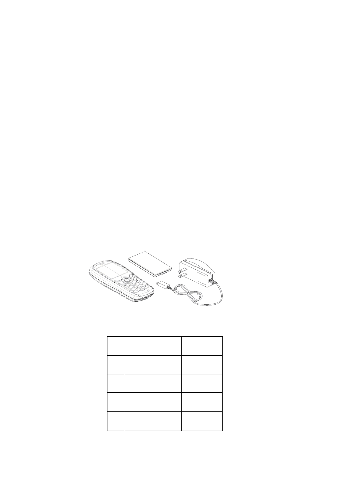
2.3. Handportable Main Kit
1
Figure 2.1: Handportable Main Unit Kit Contents
Item
1
2
3
DESCRIPTION PART NUMBER
Main Unit
770040RH01W
2
3
Battery, Standard
Travel Charger
Document Pack See Section 9
761PV11RD1W
7620003482W
– 3–1 –
3. OPERATING INSTRUCTIONS
3.1. General
This section provides a brief guide to the operation and facilities available on the telephone handset. Refer to the
Operating Instructions supplied with the telephone for full operational information.
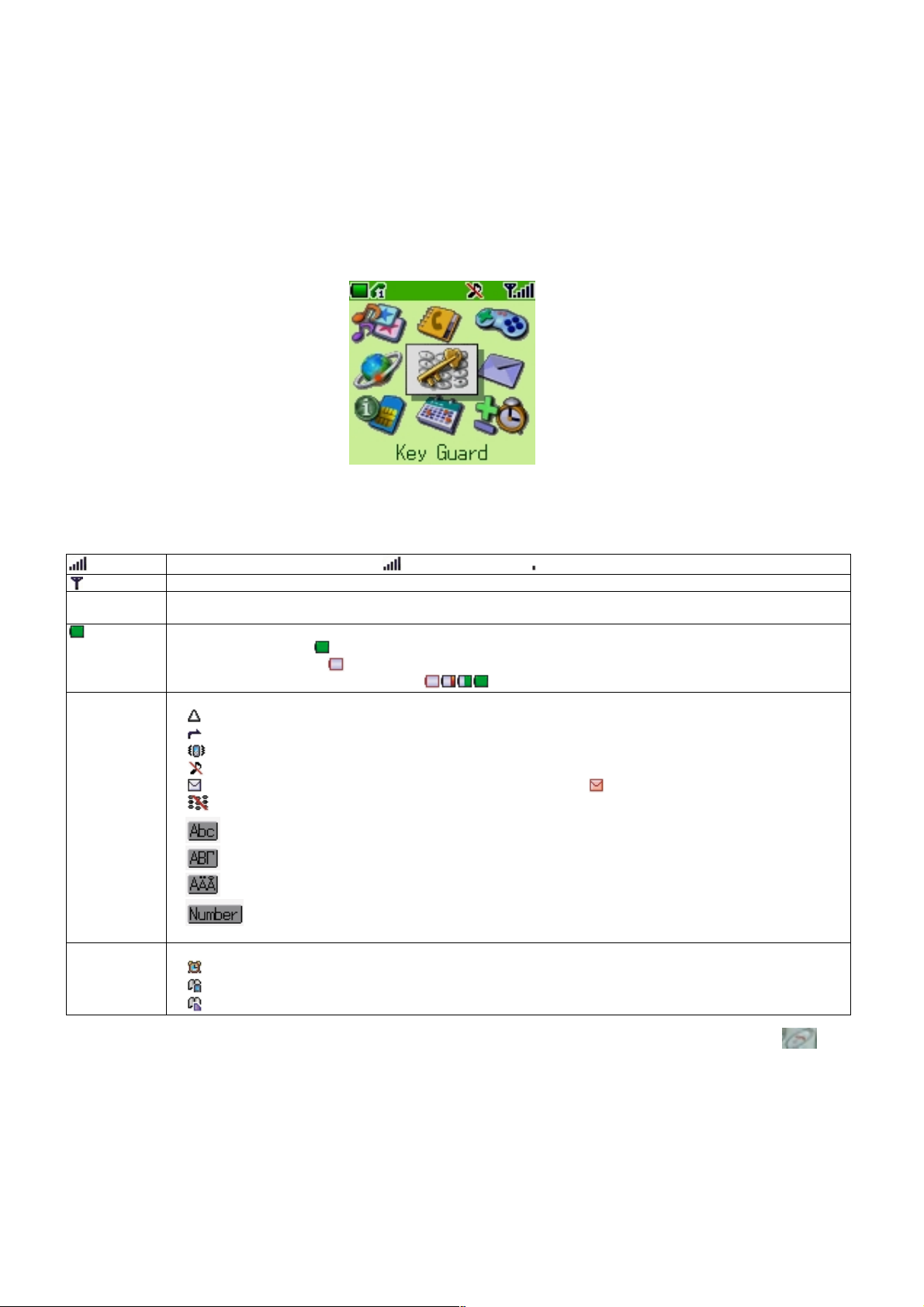
3.2. Liquid Crystal Display
The telephone handset has a graphical chip on glass display. The following icons are available:
Figure 3.1: Liquid Crystal Display
Menu Number The number of the feature indicated by the pointer. To access a feature enter the menu number on the
Menu Icon Displays a small icon related to the current status of the telephone:"
Information
Icon
Indicates received signal strength: strong signal area ; weak signal area
Indicates that it is possible to make an emergency call.
keypad.
Displays the battery charge level: "
Battery is at full charge
Battery requires charging
The battery icon flashes during charging
telephone is roaming on a non-home network.
using the “Call Divert” feature or the telephone has Call-Divert set;
shows that vibration alert is switched on;
shows that the telephone is in silent mode - no tones;
flashes to indicate that there are unread text (SMS) messages. Lit when SMS area is full;
indicates the telephone is locked;
shows that the normal character set has been selected;
shows that the Greek character set has been selected;
shows that the Extended character set has been selected;
shows that numbers have been selected for text entry
T9 indicates that Tegic T9R predictive text mode is selected
Displays a small icon according to the current menu level:
indicates the alarm is set."
indicates the current Phonebook is sourced from the Mobile Phonebook.
indicates the current Phonebook is sourced from the SIM Phonebook
Following some operations, the display will clear automatically after three seconds or after pressing any key except .
– 3–2 –
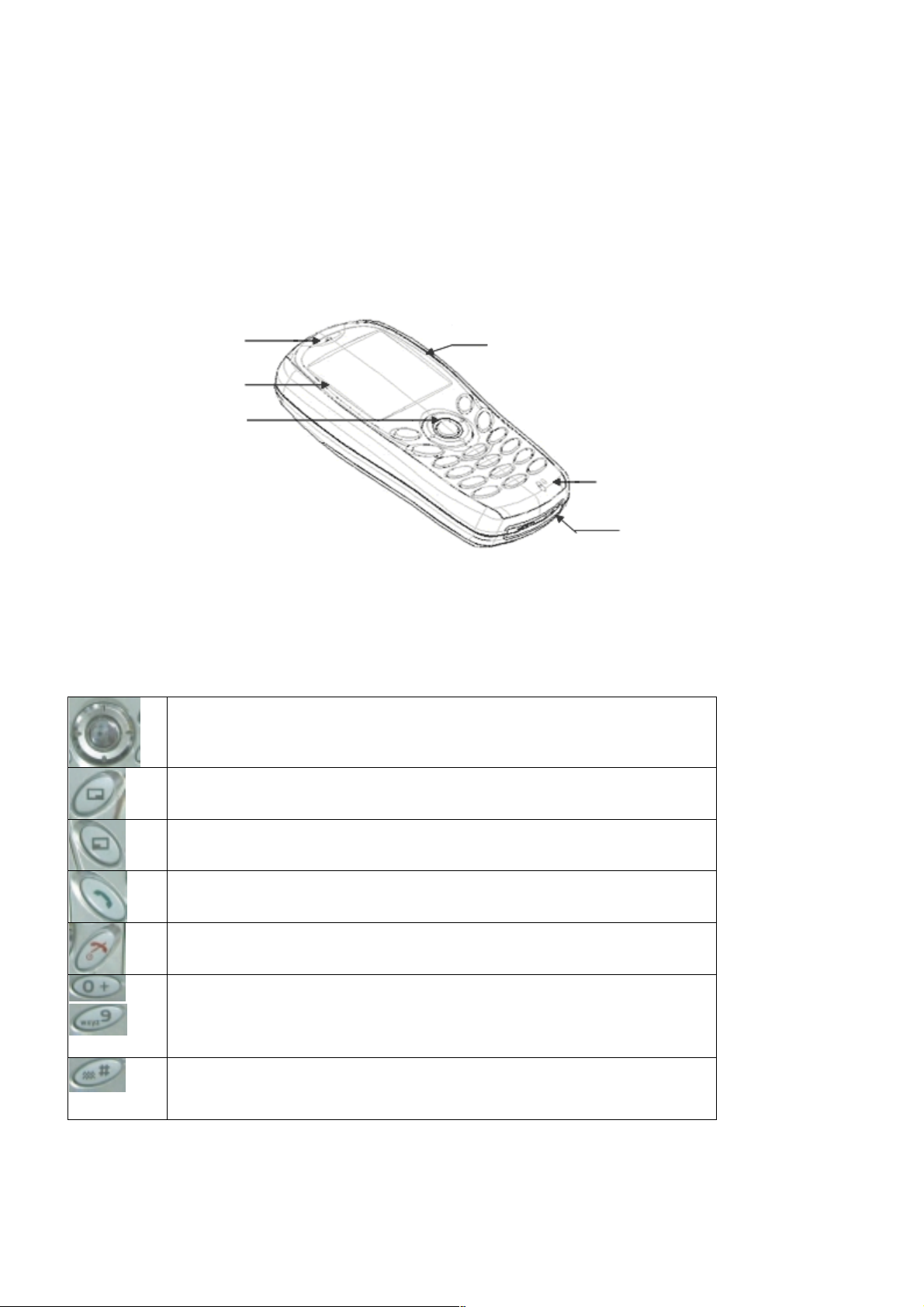
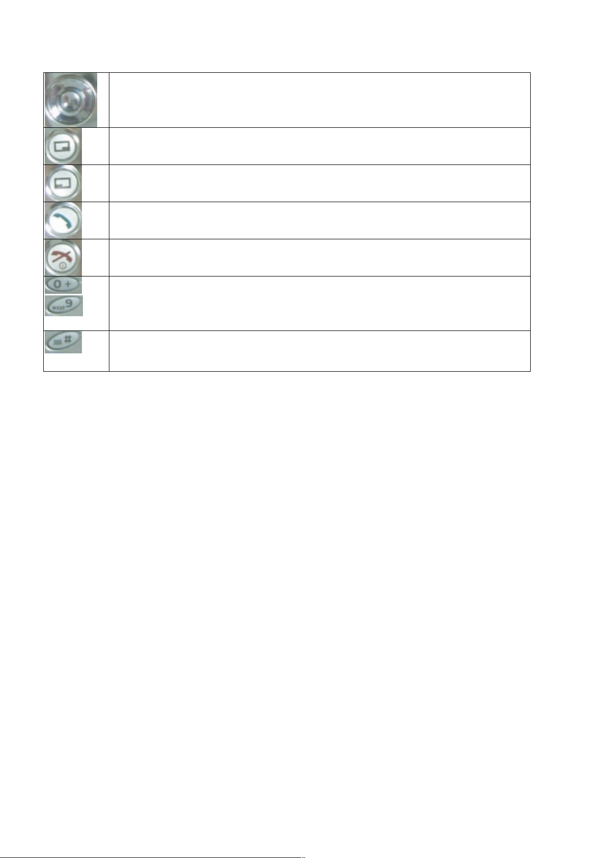
3.3. Location of Controls
Incoming / Charge indicator:
Green - Incoming call.
Red - Charging battery pack.
External connector:
Used to connect to external accessories or to charging equipment
Receiver
Display
Navigation Key
The keypad Type A
Navigation Key. Scrolls through options or features menu and increases or decreases volume.
Cancel Key. Used mainly to cancel the current operation and return to the previous menu level. In
some menus it has other functions.
Option key. Primarily used for accessing the Phonebook or switching character types.
Earphone / Microphone Socket
Figure 3.2: Location of Controls
Microphone
External Connector
Send Key. Makes a call.
End Key. Ends a call or switches the telephone on/off when pressed and held.
Digit keys. Enter wild numbers or pauses when pressed and held. Where appropriate the 0 key
scrolls up or down through abbreviated control names and then select to reveal the international
to
access code “+”.
Vibrate enable/disable Key. Press and hold to enable or disable the vibrate alert.
– 3–3 –
The keypad Type B
Navigation Key. Scrolls through options or features menu and increases or decreases volume.
Cancel Key. Used mainly to cancel the current operation and return to the previous menu level. In
some menus it has other functions.
Option key. Primarily used for accessing the Phonebook or switching character types.
Send Key. Makes a call.
End Key. Ends a call or switches the telephone on/off when pressed and held.
Digit keys. Enter wild numbers or pauses when pressed and held. Where appropriate the 0 key scrolls
to
up or down through abbreviated control names and then select to reveal the international access code
“+”.
Vibrate enable/disable Key. Press and hold to enable or disable the vibrate alert.
– 3–4 –
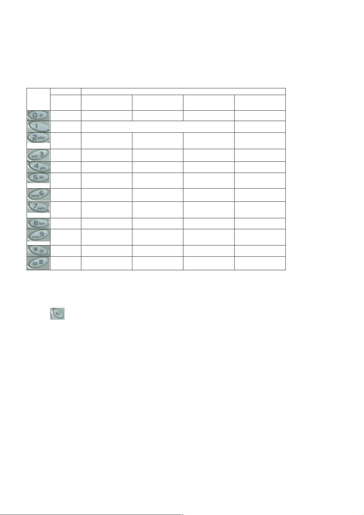
3.4. Alpha Entry
3.4.1 Character Set / Key Assignments
Alpha entry is used to enter alphanumeric characters in to the Phonebook, Short Messages and Greeting Message areas
The keypad of Type A
Character / Operation Key
T9®
Alternatives + – + – + – 0+P_
Punctuation
abc A B C a b c
def D E F d e f
ghi G H I g h i
jkl J K L j k l
Normal Greek Extended Numeric
“ @ – , . ; : ! i ? ¿ ( ) ‘ & % + – / < > = £ $ ¥ ¤ §
Α Β Γ
∆ Ε Ζ
Η Θ Ι
Κ Λ Μ
A Ä Å Æ B C Ç a ä
å æ à b c
D E É F d e é è f
G H I g h i ì
J K L j k l
1
2
3
4
5
mno M N O m n o
pqrs P Q R S p q r s
tuv T U V t u v
wxyz W X Y Z w x y z
Shift / Lock
Space # # # #
Each time a key is pressed, it will display the next character. When another key is pressed, or no key is pressed for a
short time, the cursor will move to the next position.
To cycle between Greek characters (Α Β Γ), extended characters (A Ä Å), numerals (0-9) and normal characters (A B
C) press .
∗∗∗∗
Ν Ξ Ο
Π Ρ Σ
Τ ϒ Φ
Χ Ψ Ω
M N Ñ O Ö o m n ñ
o ö ø
P Q R S p q r s ß
T U U V t u ü ù v
W X Y Z w x y z
6
7
8
9
– 3–5 –
The keypad of Type B
Key
T9R Normal Greek Extended Numeric
Alternatives + - + - + - 0+P_
Punctuation
abc A B C a b c
def D E F d e f
ghi G H I g h i
jkl J K L j k l
“ @ – , . ; : ! i ? ¿ ( ) ‘ & % + – / < > = £ $ ¥ ¤ §
Α Β Γ
∆ Ε Ζ
Η Θ Ι
Κ Λ Μ
Character / Operation
A Ä Å Æ B C Ç a ä
å æ à b c
D E É F d e é è f
G H I g h i ì
J K L j k l
1
2
3
4
5
mno M N O m n o
pqrs P Q R S p q r s
tuv T U V t u v
wxyz W X Y Z w x y z
Shift / Lock * * * *
Space # # # #
Each time a key is pressed, it will display the next character. When another key is pressed, or no key is pressed for a
short time, the cursor will move to the next position.
To cycle between Greek characters (Α Β Γ), extended characters (A Ä Å), numerals (0-9) and normal characters (A B
C) press .
Ν Ξ Ο
Π Ρ Σ
Τ ϒ Φ
Χ Ψ Ω
M N Ñ O Ö o m n ñ
o ö ø
P Q R S p q r s ß
T U U V t u ü ù v
W X Y Z w x y z
6
7
8
9
3.4.2 Editing Alpha Entry
Pressing will move the cursor up or down or left or right. When the cursor is moved over a character and another
key pressed this will insert the new character.
Pressing
will delete the character to the left of the cursor.
– 3–6 –
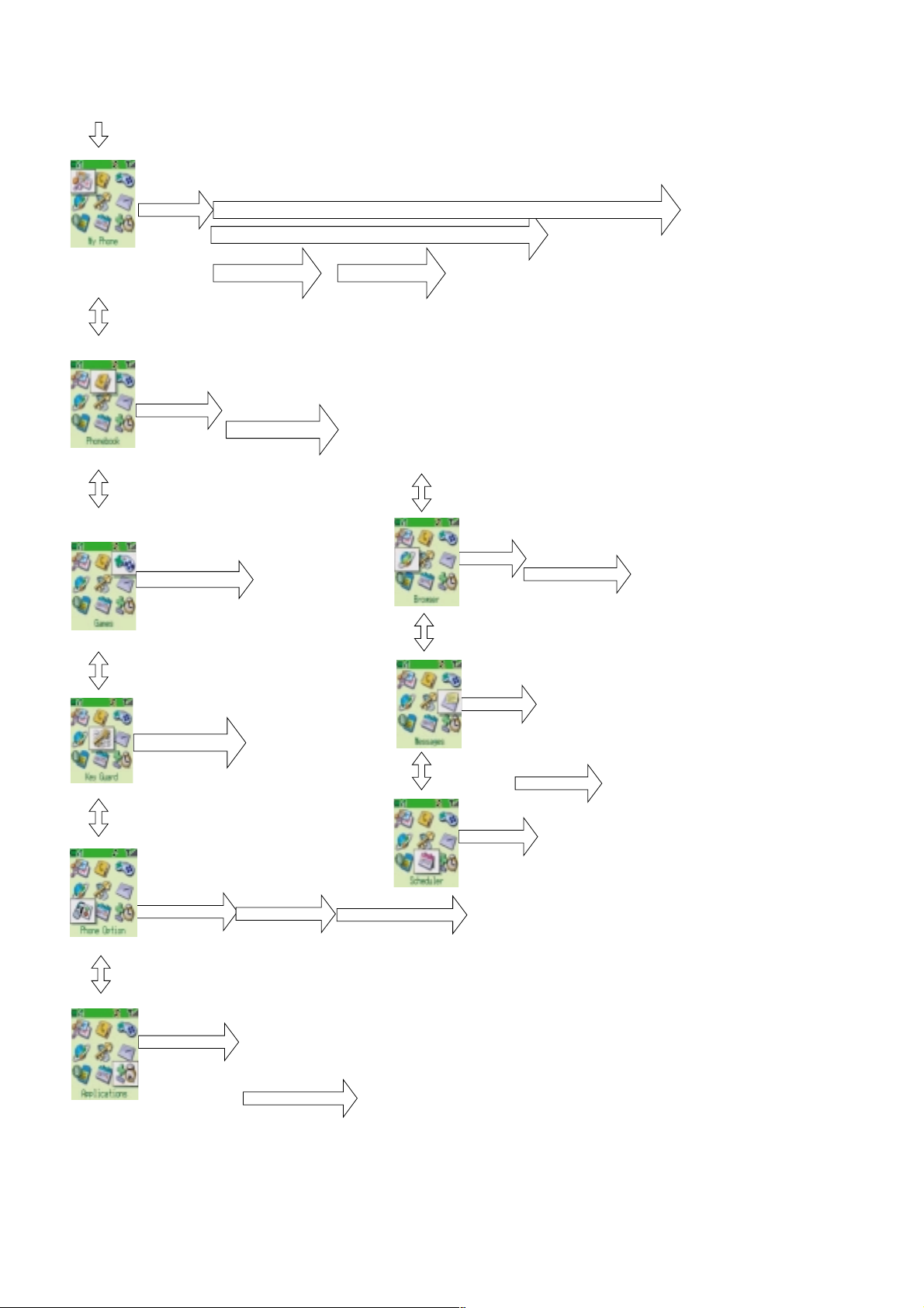
3.5. Features Menu Structure
My Phone
Phonebook
Games
Media Folder
Sound Setting
Display Setting
Quick Notice
Language
Auto Answer
Default
Browse
Create
Group Setting
Review
Copy Entries
My Number
Fixed Dial
Voicemail
Ping Ball
Black Jack
Sound Setting
Idle Screen
Screen Saver
Colour Themes
Greeting
Operator Notice
Contrast
Backlight Time
SIM Phonebook
Mobile Phnebook
Fixed Data
User Data
Browser
General Mode
Meeting Mode
Outdoor Mode
Car Mode
Party Mode
Customized Mode
Start Browse
Brower Setting
Picture
Melody
Animation
Status
Set Profile
Set GPRS
Key Guard
Phone Option
Applications
Call Services
Call Divert
Security
Network
Games
Voice Memo Play
Record
Clock Function
Calculator
Edit Ringtone
Calls
Service Changes
Connections
Show My Number
Clock Set
Clock Format
Alarm Set
Power ON Time
Power OFF Time
Messages
Scheduler
Last Call
All Calls
Call Waiting
Chat SMS
Callers ID
Withhold ID
Active Line
Create
Inbox
Outbox
Chat SMS
Broadcasts
Options
Receive
Latest message
OStore Message
Topics
Notify Tone
Topic Index
Laguages

– 3–7 –
3.6. Glossary of Terms
Term Definition
DTMF Dual Tone Multiple Frequency tones. The numeric keys 0 to 9, and * and # will
generate different DTMF tones when pressed during conversation. These are
used to access voice mail, paging and home banking services.
GSM Global System for Mobile communications. The name given to the advanced
digital technology that the telephone uses.
Home network The GSM network on which subscription details are held.
Hot Key Dial Hot Key Dial allows quick access to numbers stored in the Phonebook of Service
Dial Number list. The source of the Hot Key Dial may be defined by the user or
preprogrammed by the Service Provide. It is most likely to be preprogrammed to
the Service Dial Numbers by the Service Provider.
Lock code Used for security of the telephone. Factory set to “0000”.
Message Centre Where messages are sent before they are forwarded on to their destination. The
Message Centre telephone number may be programmed into the SIM or supplied
by the service provider.
Network operator The organisation responsible for operating a GSM network.
Password Used for the control of the call bar function. Supplied by the service provider.
PIN Personal Identification Number used for SIM security. Supplied by the service
provider.
PIN2 Personal Identification Number used for the control of Fixed Dial Memory and call
charge metering. Supplied by the service provider.
PUK/ PUK2 PIN/PIN2 Unblocking Key. Used to unblock the PIN/PIN2. Supplied by the
service provider.
Registration The act of locking on to a GSM network. This is usually performed automatically
by the telephone.
Roaming The ability to use the telephone on networks other than the Home network.
Service Dial Numbers Service Dial Numbers are predefined numbers that allow the user to access a set
of special services provided by the Service Provider. For example billing
information or access to Voice Mail.
Service provider The organisation responsible for providing access to the GSM network.
SIM Subscriber Identification Module. A small smart-card which stores unique
subscriber and user-entered information such as Phone Book, Fixed Dial
Memory and short messages. Supplied by the service provider.
Supplementary
service
Wild numbers Spaces in a stored telephone number. When the telephone number is recalled
Network-controlled GSM functions supported by the telephone. Supplementary
services may only be available on a subscription bases.
pressing a numeric key will fill in a space. This can be used to restrict dialling to a
specific area.

– 4–1 –
4. TECHNICAL SPECIFICATIONS
4.1. Tx Characteristics
All data is applicable to E-GSM 900 and GSM 1800 except where stated.
4.1.1. Frequency Error
±0.1 ppm max., relative to base station frequency.
4.1.2 Modulation Phase Error
RMS: Equal to or less than 5 °
Peak: Equal to or less than 20 °
4.1.3. Output RF Spectrum due to Modulation
Offset from Centre Frequency (kHz)
±100
±200
±250
±400
±600 to 1800
Maximum Level Relative to Carrier (dB)
4.1.4. Output RF Spectrum due to Switching Transients
Offset from Centre Frequency (kHz)
E-GSM 900 GSM 1800
±400
±600
±1200
±1800
Measurement conditions for output RF spectrum measurements:
Frequency Span 0 Hz
Maximum Level (dBm)
–19
–21
–21
–24
+0.5
–30
–33
–60
–60
–22
–24
–24
–27
Measurement Bandwidth: 30 kHz
Video Bandwidth: 30 kHz (modulation)
100 kHz (switching)
Average (Modulation) over 200 burst
Peak Hold (Switching) over 10 burst
– 4–2 –
4.1.5. Spurious Emissions at Antenna Connector
Frequency Range
100KHz to 50MHz 50 to 500MHz 500MHz to 1GHz 0 to 1MHz
1 GHz to 12.75 GHz
Excl. rel evant TX band
E-GSM:880 to 915 MHz
DCS:1710 to 1785 MHz
-and the Rx bands
925 -960 MHz
1805 - 1880 MHz
Relevant TX band:
E-GSM:880 to 915 MHz
DCS:1710 to 1785 MHz
Frequency
offset
0 to 10MHz
>10MHz
>30MHz
(off trom edge
of relevant Tx
band)
1.8 to 6.0 MHz
>6.0MHz
4.1.6. Residual Peak Power
Equal to or less than 70 dBc (BW = 300 kHz)
Filter
Bandwidth
10KHz 30KHz
100KHz 300KHz
100KHz 300KHz
100KHz
300KHz
3MHz
30KHz
100KHz
Approx
Video B/W
300KHz
1MHz
3MHz
100KHz
300KHz
Limits(dBm)
E-GSM 900 GSM1800
-36 -36
-36 -36
-36 -36
-30
-30
-30
-36
-36
-30(1.0 -1.710GH
z)
-36(1.710 -1.785
GHz)
-30(1.785 -12.75
GHz)
-36
-36
4.2. Rx Characteristics
4.2.1. Sensitivity
E-GSM 900 Full Rate Speech
The reference sensitivity performance in terms of frame erasure, bit error, or residual bit error rates (whichever is
appropriate) is specified in the following table, according to the propagation conditions.
Channels
TCH/FS FER
class Ib
(RBER)
class II
(RBER)
The reference sensitivity level is < -104 dBm.
Propagation
conditions
TU high
Tes t Limit
error rate
%
6.742* a
0.42/ a
8.333
Minimum
No of
samples
8900
10000 00
120000
Propagation
conditions
Test Limit
error rate
%
7.5
RA
Minimum
No of
samples
24000
Propagation
conditions
Test Limit
error rate
%
9.333
HT
Minimum
No of
samples
60000
Static Conditions
Test Limit
error rate
%
0.122* a
0.41/ a
2.439
164000
20000000
8200
Minimum
No of
samples
NOTE: 1 < α < 1.6. The value of a can be different for each channel condition but must remain the same for FER and class
1b RBER measurements for the same channel condition.

– 4–3 –
E-GSM 900 Half Rate Speech
The reference sensitivity performance in terms of frame erasure, bit error, or residual bit error rates (whichever is
appropriate) is specified in the following table, according to the propagation conditions.
Channels
TCH/HS(FER)
TCH/HS clas s Ib (BFI=0)
TCH/HS class II (BFI=0)
TCH/HS (UFR)
TCH/HSL class Ib ((BFI or
UFI)=0)
Propagation
conditions
TU high
Test Limit
error rate
%
4.598
0.404
7.725
6.250
0.269
Minimum
No of
samples
13050
148500
25500
9600
227000
Propagation
Test Limit
error rate
%
8.500
conditions
RA
Minimum
No of
samples
20000
Test Limit
error rate
%
7.600
Propagation
conditions
HT
Minimum
No of
samples
20000
GSM 1800 Full Rate Speech
The reference sensitivity performance in terms of frame erasure, bit error, or residual bit error rates (whichever is
appropriate) is specified in the following table, according to the propagation conditions.
Channels
TCH/FS FER
Propagation
conditions
TU high
Test Limit
error rate
%
4.478* a
Minimum
No of
samples
13400
Propagation
Test Limit
error rate
%
conditions
RA
Minimum
No of
samples
Propagation
Test Limit
error rate
%
conditions
HT
Minimum
No of
samples
Static Conditions
Test Limit
error rate
%
0.122* a
Minimum
No of
samples
164000
class Ib
(RBER)
The reference sensitivity level is < -103 dBm.
NOTE: 1 < α < 1.6. The value of a can be different for each channel condition but must remain the same for FER and class
class II
(RBER)
1b RBER measurements for the same channel condition.
0.32/ a
8.333
1500000
60000
7.5
24000
9.333
30000
0.41/ a
2.439
20000000
8200
GSM 1800 Half Rate Speech
The reference sensitivity performance in terms of frame erasure, bit error, or residual bit error rates (whichever is
appropriate) is specified in the following table, according to the propagation conditions.
Channels
TCH/HS(FER)
TCH/HS class Ib (BFI=0)
TCH/HS class II (BFI=0)
TCH/HS (UFR)
TCH/HSL class Ib ((BFI or
UFI)=0)
Propagation
conditions
TU high
Test Limit
error rate
%
4.706
0.426
7.725
6.383
0.291
Minimum
No of
samples
12750
141000
25500
9400
206000
Propagation
Test Limit
error rate
%
8.735
conditions
RA
Minimum
No of
samples
20000
Test Limit
error rate
%
7.600
Propagation
conditions
HT
Minimum
No of
samples
20000
– 4–4 –
Blocking:
Frequency
FR ± 600 kHz to FR ± 800 kHz
FR ± 800 kHz to FR± 1,6 MHz
FR ± 1,6 MHz to FR ± 3 MHz
915 MHz to FR - 3 MHz
±
3 MHz to FR 980 MHz
FR
FR ± 600 KHz to FR ± 800 KHz
1785 MHz to FR - 3 MHz
835 MHz to < 915 MHz
> 980 MHz to 1000 MHz
100 KHz to < 835 MHz
> 1000 MHz to 12.75 GHz
100 KHz to 1705 MHz
> 1705 MHz to < 1785 MHz
> 1920 MHz to 1980 MHz
> 1980 MHz to 12.75 GHz
Small MS level in dBµVemf( )
E-GSM 900 GSM 1800
70
70
80
90
90
-
113
113
90
90
-
-
-
-
70
70
80
-
87
87
-
-
-
-
113
101
101
90
Measurement Conditions:
Wanted carrier is 3 dB above reference sensitivity.
Interferer is CW.
Spurious response exceptions:
Six exceptions are permitted IN band 915 - 980 MHz.
24 exceptions are permitted OUTSIDE band 915 - 980 MHz.
Intermodulation Characteristics
Interferer Level ( f1& f2) dBm Interferer Frequencies ( f1&f2 )
-49 Wanted frequency= 2f1 - f2,
and [ f1 - f2] = 800 kHz

– 5–1 –
5. TECHNICAL DESCRIPTION
5.1. RF Overview
5.1.1. Introduction
■ General Specifications
The telephone is a Dual Band product incorporating two switch able transceivers, one for the E-GSM 900 band
and another for the GSM 1800 (DCS 1800) band. The transmit and receive bands for the mobile are given in
the table below:
Tx Rx
E-GSM 900 880 - 915 MHz 925 - 960 MHz
GSM 1800 1710 - 1785 MHz 1805 - 1880 MHz
GSM 850 824 - 849 MHz 869 - 894 MHz
GSM 1900 1850 - 1910 MHz 1930 - 1990 MHz
Other salient technical features are as follows:
E-GSM 900 GSM 1800 GSM 850 GSM 1900
Rx Bandwidth 35 MHz 75 MHz 25 MHz 60 MHz
Tx Bandwidth 35 MHz 75 MHz 25 MHz 60 MHz
Duplex Spacing 45 MHz 95 MHz 45 MHz 80 MH z
Number of Channels 174 374 124 299
AFRCN(Channel Numbers) 0 - 124
975 - 1023
1st Tx Channel 880.2 MHz
(Ch975)
Last Tx Channel 914.8MHz
(Ch124)
1st Rx Channel 925.2 MHz
(Ch 975)
Last Rx Channel 959.8 MHz
(Ch124)
Maximum Tx power 33.0dBm
{Class 4}(PL5)
Minimum Tx power 5.0dBm
(PL19)
512 - 885 128 - 251 512 - 810
1710.2 MHz
(Ch512)
1784.8 MHz
(Ch885)
1805.2 MHz
(Ch512)
1879.8 MHz
(Ch885)
30dBm
{Class 1}(PL0)
0.0dBm
(PL15)
824.2 MHz
(Ch128)
848.8 MHz
(Ch251)
869.2 MHz
(Ch128)
893.8 MHz
(Ch251)
33.0dBm
{Class 4}(PL5)
5.0dBm
(PL19)
1850.2 MHz
(Ch512)
1909.8 MHz
(Ch810)
1930.2 MHz
(Ch512)
1989.8 MHz
(Ch810)
30dBm
{Class 1}(PL0)
0.0dBm
(PL15)
■ Main PCB Description
All components required for the RF and Logic circuits, excluding the LCD module, are contained on a single
printed circuit board (PCB). The PCB has six layers with lay1-2 and layer 5-6 build-up Surface and back layer
tracks are gold-plated to prevent oxidization and enable better soldering. The PCB mother broad thickness is 1
mm ± 0.1 mm; MMI is 0.4 min ± 0.05 mm. All RF components are located on one side of the bottom half area of
the PCB, with the baseband components (Logic circuits) occupying the lower half of the PCB. A metallised shield
shields the RF circuit area. The top half of the back case has been designed to provide a shielded enclosure to
reduce further spurious emissions and logic noise.
– 5–2 –
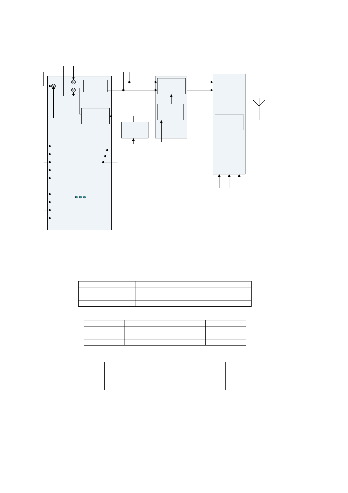
5.1.2. RF Function Block
Figure 5.1. : RF Function Block Diagram
– 5–3 –
5.1.3. Functional Description
■ Frequency Plan
The frequency plan is shown below:
TX TXIF TX UHF LO
E-GSM 900 880 - 915 MHz 88.46 - 114.35 MHz 1459.59 - 1543.725 MHz
GSM 1800 1710 - 1785 MHz 90.31 - 104.77 MHz 1354.73 - 1414.482 MHz
GSM 850 824 - 850 MHz 82.42 - 105.55 MHz 1359.93 - 1424.922 MHz
GSM 1900 1850 - 1910MHz 97.37 - 112.34 MHz 1460.68 - 1516.606MHz
RX RX LO
E-GSM 900 925 - 960 MHz 925.2 - 959.8 MHz
GSM 1800 1805 - 1880 MHz 1805.2 - 1879.8 MHz
GSM 850 869 - 894 MHz 869.2 - 893.8 MHz
GSM 1900 1930 - 1990MHz 1930.2 - 1989.8 MHz
Fig 5.2 Transmitter Frequency Generation

– 5–4 –
The CX74017 transmitter functional block diagram is shown in Figure 5.2 The transmit (Tx) chain is based on a
translational loop architecture. The baseband information is injected within the loop therefore the output signal is phasemodulate.
One of the advantages of this architecture is that the Transmit Intermediate Frequency (TxIF) is kept within a narrow
frequency range. This improves phase and amplitude accuracy in the
In-Phase and Quadrature (I/Q) modulator.
The CX74017 has two frequency dividers:
8 D1: set to divide by 9, 10, 11, or 12
8 D2: set to divide by 2 or 1
To minimize the range of the TxIF and the required tuning range of the UHF VCO, the D2 divider is set to /2 mode for low
band operation. Low band operation includes the EGSM. For high band operation, the D2 divider is set to /1 mode.High
band operation includes the DCS1800 .
The UHF VCO is divided by three. After this block, the VCO is multiplied by 1 for low band operation or multiplied by 2 for
high band operation. This block drives both the D1 divider, which feeds the phase detector, and a doubler stage, which
feeds the high side injection down converter 1/2 Local Oscillator (LO) mixer. The mixer mixes the transmit frequency
down to the TxIF frequency that drives the I/Q modulator. The output of the modulator is filtered externally and then fed
back into the CX74017 where it drives the D2 divider. The D2 divider feeds the other input of the phase detector, which
produces an error voltage that is externally filtered. The error voltage tunes the internal Transmit Voltage Controlled
Oscillator (TxVCO).
■ General
RF circuit design is built around and Skyworks CX74017 IC. Other major components include filters, power amplifiers
and the antenna subsystems.
Direct conversion is employed on both receiver bands.
The Tx VCO is on-channel in both E-GSM 900 and GSM 1800 modes of operation.
The RF LO always requires re-tuning between transmit and receive modes, as well as when monitoring adjacent cells.
■ Antenna
The antenna is an internal inverted F-type. It is optimized for both free space and talk positions on GSM 900 and GSM
1800 bands. The RF coaxial connector incorporates a mechanical switch for routing the RF signal to an external
antenna for car kit installations and for test purposes.
■ Transmit and Receive
The transmit and receive paths are covered in their own specific chapters later in this Technical Guide.

– 5–5 –
5.2. TRANSMITTER
5.2.1. Introduction
This section provides a technical description of the transmitter circuits of the Main PCB. A circuit diagram of the whole
system is provided in the Service Manual.
5.2.2. Uplink Frequencies
■ E-GSM 900
The uplink frequencies for the E-GSM 900 band are as follows:
CHANNEL
NUMBERS
975 - 979
980 - 984
985 - 989
990 - 994
995 - 999
1000 - 1004
1005 - 1009
1010 - 1014
1015 - 1019
1020 - 1024
1 - 5
6 - 10
11 - 15
16 - 20
21 - 25
26 - 30
31 - 35
36 - 40
41 - 45
46 - 50
51 - 55
56 - 60
61 - 65
66 - 70
71 - 75
76 - 80
81 - 85
86 - 90
91 - 95
96 - 100
101 - 105
106 - 110
111 - 115
116 - 120
121 - 124
880.200
881.200
882.200
883.200
884.200
885.200
886.200
887.200
888.200
889.200
890.200
891.200
892.200
893.200
894.200
895.200
896.200
897.200
898.200
899.200
900.200
901.200
902.200
903.200
904.200
905.200
906.200
907.200
908.200
909.200
910.200
911.200
912.200
913.200
914.200
880.400
881.400
882.400
883.400
884.400
885.400
886.400
887.400
888.400
889.400
890.400
891.400
892.400
893.400
894.400
895.400
896.400
897.400
898.400
899.400
900.400
901.400
902.400
903.400
904.400
905.400
906.400
907.400
908.400
909.400
910.400
911.400
912.400
913.400
914.400
UPLINK FREQUENCIES
880.600
881.600
882.600
883.600
884.600
885.600
886.600
887.600
888.600
889.600
890.600
891.600
892.600
893.600
894.600
895.600
896.600
897.600
898.600
899.600
900.600
901.600
902.600
903.600
904.600
905.600
906.600
907.600
908.600
909.600
910.600
911.600
912.600
913.600
914.600
880.800
881.800
882.800
883.800
885.800
886.800
887.800
888.800
889.800
890.800
891.800
892.800
893.800
894.800
895.800
896.800
897.800
898.800
899.800
900.800
901.800
902.800
903.800
904.800
905.800
906.800
907.800
908.800
909.800
910.800
911.800
912.800
913.800
914.800
881.000
882.000
883.000
884.000
885.000
886.000
887.000
888.000
889.000
890.000
891.000
892.000
893.000
894.000
895.000
896.000
897.000
898.000
899.000
900.000
901.000
902.000
903.000
904.000
905.000
906.000
907.000
908.000
909.000
910.000
911.000
912.000
913.000
914.000
Table 5.1
Uplink frequencies for the extended part of E-GSM 900 band (975 = ARFCN = 1023) can be calculated as follows:
Uplink frequency = 890 MHz - ((1024 - ARFCN) x 0.2 MHz) e.g. for CH984
890 MHz - 984) x 0.2 MHz)
= 890 MHz - (8 MHz)
= 882 MHz

– 5–6 –
Uplink frequencies for the standard GSM 900 band (0 = ARFCN = 124) can be calculated as follows:
Uplink frequency = 890 MHz + (ARFCN x 0.2 MHz) e.g. for CH55
890 MHz + (55 x 0.2 MHz)
= 890 MHz + (11 MHz)
= 901 MHz
■ GSM 1800
Uplink frequencies for the GSM 1800 band can be calculated as follows:
Uplink frequency = 1710 MHz + ((ARFCN - 511 MHz) x 0.2) e.g. for CH512
1710 MHz + ((512 - 511) x 0. 2MHz)
= 1710 MHz + (0.2 MHz)
= 1710.2 MHz
■ E-GSM 850
The uplink frequencies for the E-GSM 850 band are as follows:
CHANNEL
NUMBERS
128 - 132
133 - 137
138 - 142
143 - 147
148 - 152
153 - 157
158 - 162
163 - 167
168 - 172
173 - 177
178 - 182
183 - 187
188 - 192
193 - 197
198 - 202
203 - 207
208 - 212
213 - 217
218 - 222
223 - 227
228 - 232
233 - 237
238 - 242
243 - 247
248 - 251
869.200
870.200
871.200
872.200
873.200
874.200
875.200
876.200
877.200
878.200
879.200
880.200
881.200
882.200
883.200
884.200
885.200
886.200
887.200
888.200
889.200
890.200
891.200
892.200
893.200
869.400
870.400
871.400
872.400
873.400
874.400
875.400
876.400
877.400
878.400
879.400
880.400
881.400
882.400
883.400
884.400
885.400
886.400
887.400
888.400
889.400
890.400
891.400
892.400
893.400
UPLINK FREQUENCIES
869.600
870.600
871.600
872.600
873.600
874.600
875.600
876.600
877.600
878.600
879.600
880.600
881.600
882.600
883.600
884.600
885.600
886.600
887.600
888.600
889.600
890.600
891.600
892.600
893.600
869.800
870.800
871.800
872.800
873.800
874.800
875.800
876.800
877.800
878.800
879.800
880.800
881.800
882.800
883.800
884.800
885.800
886.800
887.800
888.800
889.800
890.800
891.800
892.800
893.800
870.000
871.000
872.000
873.000
874.000
875.000
876.000
877.000
878.000
879.000
880.000
881.000
882.000
883.000
884.000
885.000
886.000
887.000
888.000
889.000
890.000
891.000
892.000
893.000
Table 5.2
Uplink frequencies for the extended part of E-GSM 850 band (128 = ARFCN = 251) can be calculated as follows:
Uplink frequency = 824 MHz + ((ARFCN - 127) x 0.2 MHz) e.g. for CH128
824 MHz + ((185 - 127) x 0.2 MHz)
= 824 MHz + (11.6 MHz)
= 835.6 MHz
■ GSM 1900
Uplink frequencies for the GSM 1900 band can be calculated as follows:
Uplink frequency = 1850 MHz + ((ARFCN - 511 MHz) x 0.2) e.g. for CH680
1850 MHz + ((680 - 511) x 0. 2MHz)
= 1850 MHz + (33.8 MHz)
= 1853.8 MHz
– 5–7 –
5.2.3. Functional Description
Txin
Txqn
Txip
Txqp
PCO1
PCO2
TXENA
RXENA
SXENA
Rxin
Rxip
Rxqn
Rxqp
ÖÖ . Ö
Transceiver
CX74017
Tx-VCO
UHF-VCO
(LO)
U100
TxDCS
Fref
VCTCXO
13MHz
LE
CLK
Data
TxGSM
Dual-band
PA
PAController
U106 U104
AFC
APC
PA module
RF3140
TxGSM
TxDCS
Figure 5.3. : Functional Description
ANT
Dual-band
TR switch
U111
VC1 VC2 VC3
G60 is model using DCR (Direct Conversion Receiver) in it that eliminates the need for IF components (IF SAW), the
transceiver also integrates TXVCO and LO, and PA module integrate PAC.
1.
PCO1 PCO2 Select
0 0 No action
0 0 EGSM
1 0 DCS
2.
TXENA RXENA SXENA ACTION
1 0 1 TX
0 1 1 RX
X X 0 RF off
3.
VC1 (Pin2) VC2 (Pin4) VC3 (Pin8) ACTION
0 1 0 EGSM TX
0 0 1 DCS
0 0 0 EGSM/DCS RX
Table 5.3

– 5–8 –
The CX74017 transceiver is a highly integrated device for multi-band Global System for Mobile Communications™ (GSM ™)
or General Packet Radio Service (GPRS) applications. The device requires a minimal number of external components to
complete a GSM radio subsystem. The CX74017 supports EGSM900/DCS1800 applications.
The receive path implements a direct down-conversion architecture that eliminates the need for Intermediate Frequency (IF)
components. The CX74017 receiver consists of three integrated Low Noise Amplifiers (LNAs), a quadrature demodulator,
tunable receiver baseband filters, and a DC-offset correction sequencer.
In the transmit path, the device consists of an In-phase and Quadrature (I/Q) modulator within a frequency translation loop
designed to perform frequency up conversion with high output spectral purity. This loop also contains a phase frequency
detector, charge pump, mixer, programmable dividers, and high power transmit Voltage Controlled Oscillators (VCOs) with no
external tank required.
The charge pump output signal produced by the phase detector is fed back to the Tx VCO to generate modulated RF output.
The Tx VCO has been designed to provide a high level output thus obviating the need for a driver amplifier. Therefore, the Tx
VCO output is applied directly to the PA which amplifies the signal to any required level up to PL5 (33 dBm at the antenna) for
E-GSM 900 and PL0 (30 dBm) for GSM 1800. In the same way, the Tx VCO output is applied directly to the PA which
amplifies the signal to any required level up to PL5 (33 dBm at the antenna) for GSM 850 and PL0 (30 dBm) for GSM 1900.
The CX74017 also features an integrated, fully programmable, sigma-delta fractional-N synthesizer suitable for GPRS
multi-slot operation. Except for the loop filter, the frequency synthesizer function, including a wideband VCO, is completely
on-chip.

– 5–9 –
5.3. RECEIVER
5.3.1. Introduction
This Section provides a technical description of the receiver section of the RF circuit. A complete circuit diagram is
provided in the Service Manual.
5.3.2. Downlink Frequencies
■ E-GSM 900
The downlink frequencies for the E-GSM 900 band are as follows:
CHANNEL
NUMBERS
975 - 979
980 - 984
985 - 989
990 - 994
995 - 999
1000 - 1004
1005 - 1009
1010 - 1014
1015 - 1019
1020 - 1024
1 - 5
6 - 10
11 - 15
16 - 20
21 - 25
26 - 30
31 - 35
36 - 40
41 - 45
46 - 50
51 - 55
56 - 60
61 - 65
66 - 70
71 - 75
76 - 80
81 - 85
86 - 90
91 - 95
96 - 100
101 - 105
106 - 110
111 - 115
116 - 120
121 - 124
925.200
926.200
927.200
928.200
929.200
930.200
931.200
932.200
933.200
934.200
935.200
936.200
937.200
938.200
939.200
940.200
941.200
942.200
943.200
944.200
945.200
946.200
947.200
948.200
949.200
950.200
951.200
952.200
953.200
954.200
955.200
956.200
957.200
958.200
959.200
925.400
926.400
927.400
928.400
929.400
930.400
931.400
932.400
933.400
934.400
935.400
936.400
937.400
938.400
939.400
940.400
941.400
942.400
943.400
944.400
945.400
946.400
947.400
948.400
949.400
950.400
951.400
952.400
953.400
954.400
955.400
956.400
957.400
958.400
959.400
DOWNLINK FREQUENCIES
925.600
926.600
927.600
928.600
929.600
930.600
931.600
932.600
933.600
934.600
935.600
936.600
937.600
938.600
939.600
940.600
941.600
942.600
943.600
944.600
945.600
946.600
947.600
948.600
949.600
950.600
951.600
952.600
953.600
954.600
955.600
956.600
957.600
958.600
959.600
925.800
926.800
927.800
928.800
929.800
930.800
931.800
932.800
933.800
934.800
935.800
936.800
937.800
938.800
939.800
940.800
941.800
942.800
943.800
944.800
945.800
946.800
947.800
948.800
949.800
950.800
951.800
952.800
953.800
954.800
955.800
956.800
957.800
958.800
959.800
926.000
927.000
928.000
929.000
930.000
931.000
932.000
933.000
934.000
935.000
936.000
937.000
938.000
939.000
940.000
941.000
942.000
943.000
944.000
945.000
946.000
947.000
948.000
949.000
950.000
951.000
952.000
953.000
954.000
955.000
956.000
957.000
958.000
959.000
Table 5.4
Uplink frequencies for the extended part of E-GSM 900 band (975 = ARFCN = 1023) can be calculated as follows:
Uplink frequency = 935 MHz - ((1024 - ARFCN) x 0.2 MHz) e.g. for CH984
935 MHz - ((1024 - 984) x 0.2 MHz)
= 935 MHz - (8 MHz)
= 927 MHz

– 5–10 –
Uplink frequencies for the standard GSM 900 band (0 = ARFCN = 124) can be calculated as follows:
Uplink frequency = 935 MHz + (ARFCN x 0.2 MHz) e.g. for CH55
935 MHz + (55 x 0.2 MHz)
= 935 MHz + (11 MHz)
= 946 MHz
■ GSM 1800
Uplink frequencies for the GSM 1800 band can be calculated as follows:
Uplink frequency = 1805 MHz + ((ARFCN - 511) x 0.2 MHz) e.g. for CH512
1805 MHz + ((512 - 511) x 0. 2MHz)
= 1805 MHz + (0.2 MHz)
= 1805.2 MHz
■ GSM 850
The downlink frequencies for the GSM 850 band are as follows:
CHANNEL
NUMBERS
128 - 132
133 - 137
138 - 142
143 - 147
148 - 152
153 - 157
158 - 162
163 - 167
168 - 172
173 - 177
178 - 182
183 - 187
188 - 192
193 - 197
198 - 202
203 - 207
208 - 212
213 - 217
218 - 222
223 - 227
228 - 232
233 - 237
238 - 242
243 - 247
248 - 251
869.200
870.200
871.200
872.200
873.200
874.200
875.200
876.200
877.200
878.200
879.200
880.200
881.200
882.200
883.200
884.200
885.200
886.200
887.200
888.200
889.200
890.200
891.200
892.200
893.200
869.400
870.400
871.400
872.400
873.400
874.400
875.400
876.400
877.400
878.400
879.400
880.400
881.400
882.400
883.400
884.400
885.400
886.400
887.400
888.400
889.400
890.400
891.400
892.400
893.400
DOWNLINK FREQUENCIES
869.600
870.600
871.600
872.600
873.600
874.600
875.600
876.600
877.600
878.600
879.600
880.600
881.600
882.600
883.600
884.600
885.600
886.600
887.600
888.600
889.600
890.600
891.600
892.600
893.600
869.800
870.800
871.800
872.800
873.800
874.800
875.800
876.800
877.800
878.800
879.800
880.800
881.800
882.800
883.800
884.800
885.800
886.800
887.800
888.800
889.800
890.800
891.800
892.800
893.800
870.000
871.000
872.000
873.000
874.000
875.000
876.000
877.000
878.000
879.000
880.000
881.000
882.000
883.000
884.000
885.000
886.000
887.000
888.000
889.000
890.000
891.000
892.000
893.000
Table 5.5
Uplink frequencies for the GSM 850 band (128 = ARFCN = 251) can be calculated as follows:
Uplink frequency = 869 MHz + ((ARFCN - 127) x 0.2 MHz) e.g. for CH185
869 MHz + ((185 - 127) x 0. 2MHz)
= 869 MHz + (11.6 MHz)
= 880.6 MHz
 Loading...