

Page 1
Chip RC Networks
Type:
EZACT
EZADT
EZAST/SS
EZANT
GND GND
Type:
EZASTB/SSB
Chip RC Networks
GND
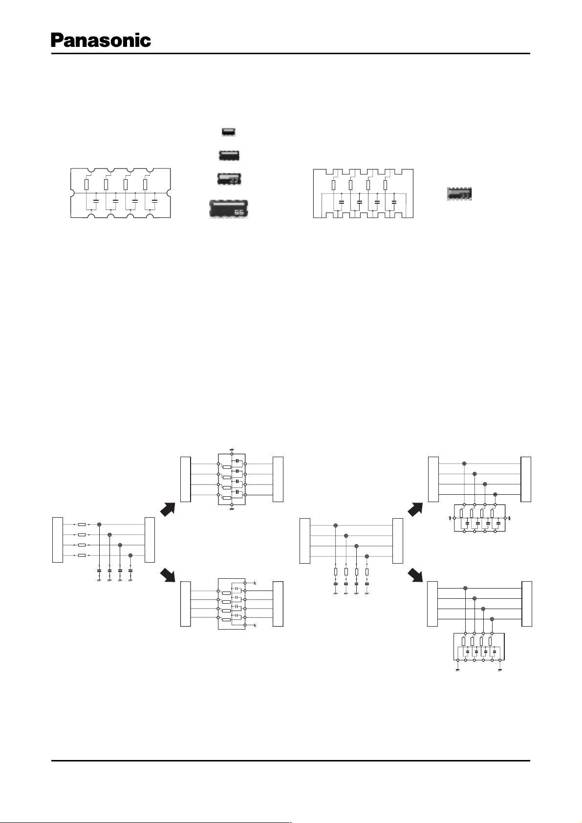
■ Features
Smallest SMD R/C networks
● 4 popular noise reduction circuits made
EZACT : 2.0 mm ҂ 1.2 mm ҂ 0.6 mm, 0.5 mm pitch (Flat terminal type)
EZADT : 3.2 mm ҂ 1.6 mm ҂ 0.65 mm, 0.635 mm pitch (Concave terminal type)
EZAST/SS : 4.0 mm ҂ 2.1 mm ҂ 0.65 mm, 0.8 mm pitch (Concave terminal type)
EZASTB/SSB : 4.0 mm ҂ 2.1 mm ҂ 0.65 mm, 0.65 mm pitch (Convex terminal type)
EZANT : 6.4 mm ҂ 3.1 mm ҂ 0.80 mm, 1.27 mm pitch (Concave terminal type)
● Takes up less space than discrete chip resistor & chip capacitor
EZACT:25 % of 0402 inches (1.0 mm ҂ 0.5 mm) chips placing area
EZADT:50 % of 0402 inches (1.0 mm ҂ 0.5 mm) chips placing area
EZAST/SS, EZASTB/SSB:70 % of 0402 inches (1.0 mm ҂ 0.5 mm) chips placing area
EZANT:55 % of 0805 inches (2.0 mm ҂ 1.2 mm) chips placing area
<Effect of high density placing, PWB space saving>
RC Low pass fi lter AC Terminator
I/O I/O
GND
I/O I/O
(EZACT, EZADT, EZAST/SS, EZANT)
I/O I/O
Discrete Chips
Chip RC Network
I/O I/O
Chip RC Network
(EZASTB/SSB)
I/O I/O
Discrete Chips
(EZACT, EZADT, EZAST/SS, EZANT)
Chip RC Network
I/O I/O
Chip RC Network
(EZASTB/SSB)
■ Recommended Applications
● Digital equipment such as PCs, printers, HDD, PCMCIA cards, PDAs, and word processors
● Communication equipment, digital cordless phones, automobile phones, GSM, PHS, DECT
● Digital audio and video equipment
● Electronic musical instruments, and other digital devices
Design and spec ifi cations are e ach subj ect to change w ithout notic e. Ask f actory for t he cur rent technical speci fi cations before purchase and/or use.
Should a sa fet y concern ar ise reg arding th is product, please be sure to c ontac t us immediately.
Feb. 2006
Page 2
■ Explanation of Part Numbers
EZACT (R/C Standard Combination)
●
1
2
3
Chip RC Networks
4
5
6
7
8
9
10
11 12
E
Thick Film Noise
Suppression and
Filtering
Components
EZADT • EZAST • EZANT (R/C Standard Combination)
●
1
E
Thick Film Noise
Suppression and
Filtering
Components
Z
Common Code
CT
2
Z
Common Code
3.2 mm
DT
҂1.6 mm
4.0 mm
ST
҂2.1 mm
6.4 mm
NT
҂3.1 mm
A
2.0 mm
҂1.2 mm
3
A
C
Dimension and
Circuit Configuration
Chip RC
Networks
4
S
Dimension and
Circuit Configuration
Chip RC
Networks
T
0
1
2
3
4
5
6
5
T
Resistance Value
Configuration
1
2
3
4
5
6
Resistance Value
Configuration
✽ 220 pF to 1000 pF available for EZANT, 22 pF to 100 pF available for EZAST, EZADT
•
EZACT
●
EZADT • EZASS • EZANT (R/C Except the standard Combination)
1
2
3
4
5
3
R/C Standard Combination
10 액
22 액
47 액
100 액
220 액
470 액
1k액
6
3
R/C Standard Combination
22 액
47 액
100 액
220 액
470 액
1k액
6
0
Capacitance Value
Configuration
0
1
7
3
Capacitance Value
Configuration
1
2
3
4
5
6
7
A
10 pF
22 pF
8
A
22 pF
47 pF
100 pF
220 pF
470 pF
1000 pF
8
A
Design
Configuration
9
A
Design
Configuration
✽
AAA
9
AAA
A
10
A
Standard
10
Resistance
Tolerance
Standard
11 12
J
Resistance
Tolerance
J
Suffix for Special
Requirement
J ±5%
Suffix for Special
Requirement
J ±5%
11 12
E
Thick Film Noise
Suppression and
Filtering
Components
EZASTB (R/C Standard Combination)
●
1
E
Thick Film Noise
Suppression and
Filtering
Components
Z
Common Code
2
Z
Common Code
4.0 mm
STB
҂2.1 mm
CT
DT
SS
NT
A
2.0mm
҂1.2 mm
3.2 mm
҂1.6 mm
4.0 mm
҂2.1 mm
6.4 mm
҂3.1 mm
3
A
Convex
terminal type
Chip RC
Networks
S
Dimension and
Circuit Configuration
4
S
Circuit Configuration
S
Chip RC
Networks
5
T
Dimension and
Resistance Value
Configuration
1
2
3
4
5
6
7
CT
DT
SS
NT
6
B
22 액
47 액
100 액
220 액
470 액
1k액
0
Resistance Value : 10 액 to 100 k액
Capacitance Value : 10 pF to 33 pF
In above-mentioned range, it is possible to
choose optional R/C.
Resistance Value : 10 액 to 100 k액
Capacitance Value : 10 pF to 100 pF
In above-mentioned range, it is possible to
choose optional R/C.
Resistance Value : 10 액 to 100 k액
Capacitance Value : 10 pF to 180 pF
In above-mentioned range, it is possible to
choose optional R/C.
Resistance Value : 10 액 to 100 k액
Capacitance Value : 220 pF to 1000 pF
In above-mentioned range, it is possible to
choose optional R/C.
7
3
R/C Standard Combination
Capacitance Value
Configuration
1
2
3
1
Design Number
8
3
22 pF
47 pF
100 pF
Y
9
A
Design
Configuration
AA
A
10
A
Standard
J
Resistance
Tolerance
J
11 12
J
Resistance
Tolerance
Suffix for Special
Requirement
±5%
Suffix for Special
Requirement
J ±5%
Design and spec ifi cations are e ach subj ect to change w ithout notic e. Ask f actory for t he cur rent technical speci fi cations before purchase and/or use.
Should a sa fet y concern ar ise reg arding th is product, please be sure to c ontac t us immediately.
Feb. 2006
Page 3
■ Explanation of Part Numbers
● EZASSB (R/C Except the standard Com bi na tion)
1
2
3
4
5
Chip RC Networks
6
7
8
9
10
11 12
E
Thick Film Noise
Suppression and
Filtering
Components
■ Construction
Protective coating
Marking
Z
Common Code
A
SSB
S
Dimension and
Circuit Configuration
Convex
4.0 mm
҂2.1 mm
terminal type
Chip RC
Networks
S
B
7
Resistance Value : 10 액 to 100 k액
Capacitance Value : 10 pF to 180 pF
In above-mentioned range, it is possible to
choose optional R/C.
0
Design Number
1
A
J
Resistance
Tolerance
J ±5%
EZACT EZADT EZAST/SS
Marking
Electrode
(Outer)
GND
Electrode
(Outer)
Alumina substrate
GND
Electrode
(Outer)
Protective coating
Electrode
(Outer)
Electrode
(Outer)
Alumina substrate
GND
Electrode
(Outer)
Alumina substrate
GND
Electrode
(Outer)
Protective coating
EZANT EZASTB/SSB
Suffix for Special
Requirement
Marking
33
GND
Electrode
(Outer)
Alumina substrate
GND
Electrode
(Outer)
Protective coating
Marking
Electrode
(Outer)
GND
Electrode
(Outer)
■ Circuit Confi guration
EZACT EZADT
10 9 8 7
GND GND
R1 R2 R3 R4
C1 C2 C3 C4
2345
R1=R2=R3=R4
C1=C2=C3=C4
61
Marking
GND
Electrode
(Outer)
Protective coating
•
EZAST/SS
10 9 8 7
GND GND
R1C1R2C2R3 R4
2345
R1=R2=R3=R4
C1=C2=C3=C4
33
Electrode
(Outer)
Alumina substrate
GND
Electrode
(Outer)
•
EZANT EZASTB/SSB
C3 C4
61
10 9 8 7
1112
R1C1R2C2R3 R4
C3
234 5 61
C1=C2=C3=C4
C4
GNDGND R1=R2=R3=R4
Design and spec ifi cations are e ach subj ect to change w ithout notic e. Ask f actory for t he cur rent technical speci fi cations before purchase and/or use.
Should a sa fet y concern ar ise reg arding th is product, please be sure to c ontac t us immediately.
Feb. 2006
Page 4

■ Dimensions in mm(not to scale)
EZACT EZADT
8710 9
Chip RC Networks
0.33±0.10
8710 9
0.20±0.15
0.5±0.2
0.4±0.2
0.40±0.150.40±0.15
23
0.5±0.1
45
2.0±0.1
61
1.25±0.10
0.25±0.15
0.55±0.10
0.30±0.15
0.25±0.15
0.40±0.15
0.635±0.100
0.35±0.15 0.35±0.10
0.45±0.15
Size : 0805 inches
Mass (Weight) [1000 pcs.] :4 g
EZAST/SS EZANT
0.5±0.2
8710 9
1
0.8±0.2
1.27±0.10
0.5±0.2
0.8±0.1
4.0±0.2
33
4523
0.45±0.20
61
0.25±0.20
0.65
2.1±0.2
+
0.20
–
0.10
3.20±0.15
6.4±0.2
0.75±0.20
61
0.2±0.1
4523
0.40±0.15
0.65
1.60±0.15
+
0.20
–
0.10
Size : 1206 inches
Mass (Weight) [1000 pcs.] :11 g
8710 9
6
0.25±0.20
4523
0.65±0.20
0.80
3.1±0.2
+
0.20
–
0.10
0.5±0.2
0.65±0.10
+
0.275
–
Size : 1608 inches
Mass (Weight) [1000 pcs.] :17 g
EZASTB/SSB
0.58±0.2
0.4±0.2
10 9 8 7
11
12
33
12 345 6
4.0±0.2
+
0.200
0.100
0.2
0.2
–
0.1
Size : 1608 inches
Mass (Weight) [1000 pcs.] :18 g
0.25±0.15
0.4±0.2
0.3±0.2
0.35±0.20
0.65
0.9±0.2
0.55±0.20
Size : 2512 inches
Mass (Weight) [1000 pcs.] :55 g
2.2±0.2
+
0.20
–
0.10
Design and spec ifi cations are e ach subj ect to change w ithout notic e. Ask f actory for t he cur rent technical speci fi cations before purchase and/or use.
Should a sa fet y concern ar ise reg arding th is product, please be sure to c ontac t us immediately.
Feb. 2006
Page 5

Chip RC Networks
■ Ratings
Item Specifi cation
Resistance Values
EZAC Standard : 10 액, 22 액, 47 액, 100 액, 220 액, 470 액, 1 k
EZAD/S/N Standard : 22 액, 47 액, 100 액, 220 액, 470 액, 1 k
Resistance Tolerance ±5 %
Temperature Coeffi cient of Resistance (T.C.R.) ±200 ҂ 10
10 액 to 100 k
Resistor
Rated Power
Limiting Element Voltage (Maximum Rated Continuous Working Voltage)
EZAC : 0.031 W(<70 °C
EZAD/S/N : 0.063 W(<70 °C
25 V
EZAC : 10 pF to 33 pF
Standard : 10 pF, 22 pF
Capacitance Values
(25 °C, 1 kHz
(3)
, 1 Vrms)
EZAD : 10 pF to 100 pF
EZAS : 10 pF to 180 pF
Standard : 22 pF, 47 pF, 100 pF
EZAN : 220 pF to 1000 pF
Standard : 220 pF, 470 pF, 1000 pF
Capacitance Tolerance +30 %/–20 %
Capacitance Temperature Characteristics E Characteristic: +20 %/–55 %(–25 to +85 °C)
Capacitor
Dissipation Factor Less than 3 %(25, 1 kHz
EZAC, EZAD : 12 V
Rated Voltage
EZAS : 25 V
EZAN : 50 V
Category Temperature Range (Operating Temperature Range)
(1) For resistors operated in ambient temperature above 70 °C, rated power shall be derated. (“Power Derating Curve” is shown below)
(2) Rated Voltage for resistor shall be determined from 앀Rated Power҂Resistance Value, or Limiting Element Voltage (Max. Rated Continuous Working
Voltage) whichever less.
(3) In measuring at 1 MHz, Capacitance and Dissipation Factor are different.
Power Derating Curve
For resistors operated in ambient temperatures above
70 °C, power rating shall be derated in accordance
with the fi gure on the right.
Rated Load (%)
100
80
60
40
20
0
30
20 10
–25 °C to +85 °C
0102030405060708090
Ambient Temperature (°C)
■ Attenuation Characteristics
액
–6
/°C(ppm/°C)
(2)
(3)
(1)
)
(1)
)
, 1 Vrms)
70 °C
액
액
85 °C
EZACT
●
10
0
–10
–20
–30
–40
–50
•
EZST
●
Measurement Circuit
EZASTB
0
10
20
30
Attenuation (dB) Attenuation (dB)
40
50
1M 10M 100 M 1 G
50 액
Frequency (Hz)
EZACT
EZADT
EZAST
EZASTB
EZANT
~
100
100 액 /22pF
100 액 /
액 /10pF
100 액 /4
100 pF
50 액
100 액 /22pF
7pF
촞
3G
●
10
20
30
40
50
●
10
20
30
40
50
60
Attenuation (dB) Attenuation (dB)
70
80
0
0
EZADT
EZANT
1M
100 액 /22pF
10
100
0
액 /47pF
액 / 100 pF
100M 3G1G10M1M1M 10M 100M 1G 3G
Frequency (Hz)Frequency (Hz)
1k액 /330 pF
1k액 / 1000 pF
10M 100M 1G
Frequency (Hz)
Design and spec ifi cations are e ach subj ect to change w ithout notic e. Ask f actory for t he cur rent technical speci fi cations before purchase and/or use.
Should a sa fet y concern ar ise reg arding th is product, please be sure to c ontac t us immediately.
Feb. 2006
Page 6

■ Packaging Methods (Taping)
● Standard Quantity
Type Kind of Taping Pitch (P1) Quantity
EZACT
EZADT
EZAST/SS
EZASTB/SSB
EZANT
Punched Carrier Taping
Embossed Carrier Taping 4000 pcs./reel
Chip RC Networks
5000 pcs./reel
4 mm
● Carrier Tape
fD
0
B
T
T
A
Type A B W F E P
EZACT
EZADT
EZAST/SS
EZASTB/SSB
EZANT
1.65
2.00
2.50
3.50
±0.15
±0.20
±0.20
±0.20
2.40
3.60
4.40
6.80
±0.20
±0.20
±0.20
±0.20
8.00
12.00
±0.20
±0.30
3.50
5.50
±0.05
±0.20
1.75
1.75
● Taping Reel
T
f C
±0.10
±0.20
P
P
2
1
1
±0.10
4.00
2.00
Type
EZACT
EZADT
EZAST/SS
EZASTB/SSB
EZANT
(Unit : mm)
P
0
E
F
W
fD1(Only Emboss)
P
2
±0.05
f
180.0
A
4.00
+0
–3.0
P
0
±0.10
f
D
0
+0.10
1.50
−0
f
B
60 min. 13.0
T
±0.05
0.85
±0.20
1.15
±0.20
1.30
f
CW T
9.0
±1.0
13.0
±1.0
±1.0
f
D
1
—
+0.10
1.50
−0
(Unit : mm)
±2.0
11.4
±2.0
15.4
f B
f A
Design and spec ifi cations are e ach subj ect to change w ithout notic e. Ask f actory for t he cur rent technical speci fi cations before purchase and/or use.
Should a sa fet y concern ar ise reg arding th is product, please be sure to c ontac t us immediately.
W
Feb. 2006
Page 7

■ Recommended Land Pattern Design
EZACT
●
d
g
Pb
Chip RC Networks
Land pattern
abcd
e
a
Dimensions
(mm)
0.75 0.25 1.70 0.35
EZADT
●
EZAST/SS
●
f1
c
h
Dimensions
(mm)
b
P
Land pattern
ehgP
1.85 2.60 0.25 0.60
abcd
Dimensions
f
d
a
(mm)
0.9 to 1.1 0.2 to 0.3 2.6 to 2.8 0.3 to 0.4
fgP
c
g
f2
c
Dimensions
(mm)
2.0 to 2.6 3.6 to 4.2 0.635
Solder resistant
Land pattern
abcd
d
a
e
GND
Dimensions
(mm)
1.2 to 1.4 0.4 3.1 to 3.3 0.4 to 0.5
ef1f2P
Dimensions
(mm)
b P
0.8 2.9 to 3.3 4.8 to 5.2 0.8
EZASTB/SSB
●
EZANT
●
a
f1
d
f2
GND
c
g
Pc db
Pb
f
a
• Design to make GND pattern as large as possible, because high
frequency noise is removed from GND terminals of chip RC network.
Land pattern
Dimensions
(mm)
Dimensions
(mm)
Land pattern
Dimensions
(mm)
Dimensions
(mm)
abcd
1.4 to 1.6 0.35 0.45 0.3
f1 f2 P
2.7 to 3.5 3.8 0.65
abcd
2.3 to 2.5 0.4 to 0.6 5.6 to 5.8 0.4 to 0.8
fgP
4.3 to 4.7 7.6 to 8.0 1.27
Design and spec ifi cations are e ach subj ect to change w ithout notic e. Ask f actory for t he cur rent technical speci fi cations before purchase and/or use.
Should a sa fet y concern ar ise reg arding th is product, please be sure to c ontac t us immediately.
Feb. 2006
Page 8

Chip RC Networks
■ Recommended Soldering Conditions
Recommendations and precautions are described below.
Recommended soldering conditions for refl ow
●
·R
efl ow soldering shall be performed a maximum of
two times.
·Please contact us for additional information when
used in conditions other than those specifi ed.
·Please measure the temperature of the terminals and
study every kind of solder and printed circuit board
for solderability be fore actual use.
Peak
Preheating
Temperature
Flow Soldering
●
Time
Heating
We do not recommend fl ow soldering to the prod uct, because solder bridging may occur due to the
narrow pitch of the terminals and the characteristics of the product may be badly affected when using
adhesive to affi x it to a circuit board.
For soldering (Example : Sn/Pb)
Te mperature Time
Preheating 140 °C to 160 °C 60 s to120 s
Main heating Above 200 °C 30 s to 40 s
Peak 235 ± 5 °C max. 10 s
For lead-free soldering (Example : Sn/Ag/Cu)
Te mperature Time
Preheating 150 °C to 180 °C 60 s to 120 s
Main heating Above 230 °C 30 s to 40 s
Peak max. 260 °C max. 10 s
This product has circuits on both sides. Therefore, do not use
adhesives because they may impair the products characteristics.
Safety Precautions
The following are precautions for individual products. Please also refer to the precautions common to EMI Filters,
Fuses, and Sensors(MR Elements) shown on page EX2 of this catalog.
1. Take measures against mechanical stress during and after mounting of Chip RC Networks (hereafter called the RC networks)
so as not to damage their electrodes and protective coatings.
Be careful not to misplace the RC networks on the land patterns. Otherwise, solder bridging may occur.
2. Do not use halogen-based or other high-activity fl ux. Otherwise, the residue may impair the RC networks' performance
and/or reliability.
3. Perform suffi cient preheating so that the difference of the solder temperature and the RC networks chip surface
temperature becomes 100 °C or less. Maintain the temperature difference within 100 °C during rapid cooling by
immersion into solvent after soldering.
4. When soldering with a soldering iron, never touch the RC networks' bodies with the tip of the soldering iron. When
using a soldering iron with a high temperature tip, fi nish soldering as quickly as possible (within three seconds at
350 °C max.).
5. As the amount of applied solder becomes larger, the mechanical stress applied to the RC networks increases, causing
problems such as cracks and faulty characteristics. Avoid applying an excessive amounts of solder.
6. Do not apply shock to the RC networks or pinch them with a hard tool (e.g. pliers and tweezers). Otherwise, the RC networks'
protective coatings and bodies may be chipped, affecting their performance.
7. Avoid excessive bending of printed circuit boards in order to protect the RC networks from abnormal stress.
8. The static capacitance may decrease by a few percent from the time of shipment due to the characteristics peculiar to
dielectric materials having a high dielectric constant.
Design and spec ifi cations are e ach subj ect to change w ithout notic e. Ask f actory for t he cur rent technical speci fi cations before purchase and/or use.
Should a sa fet y concern ar ise reg arding th is product, please be sure to c ontac t us immediately.
Feb. 2006
Page 9

Safety Precautions (Common precautions for EMI Filters, Fuses, and Sensors[MR Elements])
• When using our products, no matter what sort of equipment they might be used for, be sure to make a written
agreement on the specifi cations with us in advance. The design and specifi cations in this catalog are subject
to change without prior notice.
• Do not use the products beyond the specifi cations described in this catalog.
• This catalog explains the quality and performance of the products as individual components. Before use, check
and evaluate their operations when installed in your products.
• Install the following systems for a failsafe design to ensure safety if these products are to be used in equip ment
where a defect in these products may cause the loss of human life or other signifi cant dam age, such as damage to
vehicles (automobile, train, vessel), traffi c lights, medical equipment, aerospace equipment, electric heating
appliances, combustion/gas equipment, rotating equipment, and disaster/crime prevention equipment.
Systems equipped with a protection circuit and a protection device
✽
Systems equipped with a redundant circuit or other system to prevent an unsafe status in the event of a sin gle fault
✽
(1) Precautions for use
• These products are designed and manufactured for general and standard use in general elec tron ic equipment
(e.g. AV equipment, home electric appliances, offi ce equipment, information and communication equipment)
• These products are not intended for use in the following special conditions. Before using the products,
carefully check the effects on their quality and performance, and determine whether or not they can be used.
1. In liquid, such as water, oil, chemicals, or organic solvent
2. In direct sunlight, outdoors, or in dust
2
3. In salty air or air with a high concentration of corrosive gas, such as Cl
, H2S, NH3, SO2, or NO
4. Electric Static Discharge (ESD) Environment
These components are sensitive to static electricity and can be damaged under static shock (ESD).
Please take measures to avoid any of these environments.
Smaller components are more sensitive to ESD environment.
5. Electromagnetic Environment
Avoid any environment where strong electromagnetic waves exist.
6. In an environment where these products cause dew condensation
7. Sealing or coating of these products or a printed circuit board on which these products are mounted, with
resin or other materials
• These products generate Joule heat when energized. Carefully position these products so that their heat will
not affect the other components.
• Carefully position these products so that their temperatures will not exceed the category temperature range due
to the effects of neighboring heat-generating components. Do not mount or place heat-generating components
or infl ammables, such as vinyl-coated wires, near these products (except Thermal Cutoffs).
• Note that non-cleaning solder, halogen-based highly active fl ux, or water-soluble fl ux may deteriorate the
performance or reliability of the products.
• Carefully select a fl ux cleaning agent for use after soldering. An unsuitable agent may deteriorate the performance
or reliability. In particular, when using water or a water-soluble cleaning agent, be careful not to leave water
residues. Otherwise, the insulation performance may be deteriorated.
2
(2) Precautions for storage
The performance of these products, including the solderability, is guaranteed for a year from the date of ar riv al
at your company, provided that they remain packed as they were when delivered and stored at a tem per a ture
of 5 °C to 35 °C and a relative humidity of 45 % to 85 %. (Micro Chip Fuses: Guaranteed for 6 months from the
date of arrival at your company)
The performance of EMI Filters is guaranteed for 6 months or a year from the out go ing inspection date indicated on
the packages, provided that they are stored at a temperature of -5 °C to +40 °C and a relative humidity of 40 %
to 60 %. Check the guarantee period in the specifi cations. The performance of Thermal Cut offs is guaranteed for a
year from the outgoing inspection date indicated on the packages, provided that they are stored at a temperature of
-10 °C to +40 °C and a relative humidity of 30 % to 75 %.
Even within the above guarantee periods, do not store these products in the following conditions. Otherwise,
their electrical performance and/or solderability may be deteriorated, and the packaging materials (e.g. taping
materials) may be deformed or deteriorated, resulting in mounting failures.
1. In salty air or in air with a high concentration of corrosive gas, such as Cl
2
, H2S, NH3, SO2, or NO
2
2. In direct sunlight
<Package markings>
Package markings include the product number, quantity, and country of origin.
In principle, the country of origin should be indicated in English.
Feb. 2006
– EX2 –
 Loading...