

Page 1
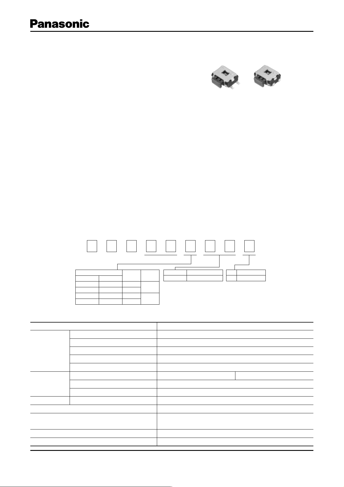
Small-sized Side- operational SMD
Light Touch Switches
Typ e:
EVQPU
■ Features
● External dimensions : 4.7 mm҂3.5 mm, Height 1.65 mm
● A wide range of terminal type : J-bent, Straight
■ Recommended Applications
● Car navigation, Car audio
Light Touch Switches/EVQPU
■ Explanation of Part Numbers
1
E
Without Boss
A
B
J
K
6th
With Boss
2
V
C
D
L
M
3 4 5 6 789
Q
Terminal
Type
Straight
J-bent
Straight
J-bent
PU 0 2K
Type
Operating
Force
2.2 N
1.6 N
7th & 8th02Mounting Height
1.65 mm
9thKPush Plate Color
Black
■ Specifi cations
Type Snap action / Push-on type SPST
Rating 10 µA 2 Vdc to 50 mA 12 Vdc (Resistive load)
Contact Resistance 500 m액 max.
Electrical
Mechanical
EnduranceOperating Life 100000 cycles min.
Operating Temperature –40 °C to +85 °C
Storage Tem per a ture
Minimum Quantity/Packing Unit 4000 pcs. Embossed Taping (Reel Pack)
Quantity/Carton 20000 pcs.
Insulation Resistance 100 M액 min. (at 100 Vdc)
ielectric With stand ing Voltage
D
250 Vac for 1 minute
Bouncing 10 ms max. (ON, OFF)
Operating Force 1.6 N
Travel 0. 3 mm
+0.7
N2.2 N
+0.1
–0.2
mm
Push Strength 30 N (1 minute)
–40 °C to +85 °C (Bulk)
–20 °C to +60 °C (Taping)
+0.8
–0.7–0.4
N
Design and specifi cations are each subject to change without notice. Ask factory for the current technical specifi cations before purchase and/or use.
Should a safety concern arise regarding this product, please be sure to contact us immediately.
Jun. 2008
Page 2
1.65
+0.3
–0.1
6.4
4.7±0.1
4.5
3.5
1
2
3
4
2.6
1.4±0.1
0.6±0.1
1.7±0.1
3.7
1
2
3
4
6.8±0.1
0.7
±
0.1
2.7±0.1
3.7±0.1
0.2±0.1
0.5
±
0.1
φ0.2±0.1
φ0.65
2.75±0.05
φ0.75
+0.1
–
0
+0
–0.3
+0
–0.2
2.75±0.10
Circuit diagram
PWB land pattern for reference
1.65
+0.30
–0.10
6.4
4.7±0.1
4.5
3.5
1
2
3
4
2.6
1.4±0.1
0.6±0.1
1.7±0.1
3.7
1
2
3
4
6.8±0.1
0.7±0.1
2.7±0.1
3.7±0.1
+0
– 0.3
Circuit diagram
PWB land pattern for reference
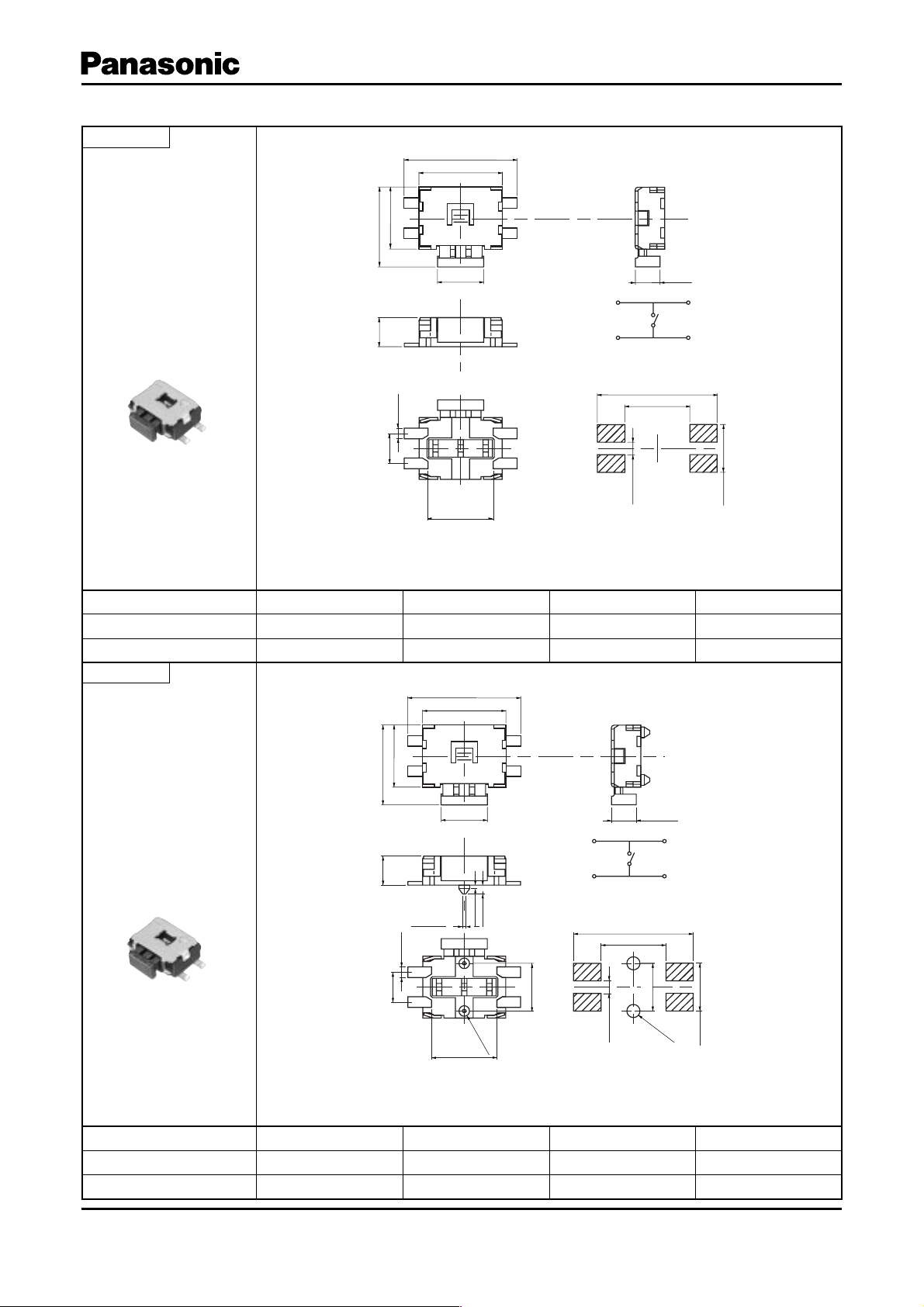
■ Dimensions in mm (not to scale)
No. 1
EVQPUJ
EVQPUA
(Embossed Tapin g)
With straight terminals
Without boss
Light Touch Switches/EVQPU
Part Numbers Operating Force Height Push Plate Color Operating Life
EVQPUJ02K1.6 N1.65 mm Black100000 cycles
EVQPUA02K2.2 N1.65 mm Black100000 cycles
No. 2
EVQPUL
EVQPUC
(Embossed Tapin g)
With straight terminals
With boss
Part Numbers Operating Force Height Push Plate Color Operating Life
EVQPUL02K 1.6 N 1.65 mm Black 100000 cycles
EVQPUC02K 2.2 N 1.65 mm Black 100000 cycles
Design and specifi cations are each subject to change without notice. Ask factory for the current technical specifi cations before purchase and/or use.
Should a safety concern arise regarding this product, please be sure to contact us immediately.
Apr. 2008
Page 3

■ Dimensions in mm (not to scale)
No. 3
EVQPUK
EVQPUB
(Embossed Tapin g)
With J-bent terminals
Without boss
4.5
3.5
Light Touch Switches/EVQPU
+0
5.5
–
0.3
4.7±0.1
3
4
1
2
1.4±0.1
1
2
+0.3
– 0.1
1.65
2.6
3
4
Circuit diagram
6.6±0.1
3.7±0.1
0.6±0.1
1.7±0.1
3.7
0.7±0.1
PWB land pattern for reference
2.7±0.1
Part Numbers Operating Force Height Push Plate Color Operating Life
EVQPUK02K1.6 N1.65 mm Black100000 cycles
EVQPUB02K2.2 N1.65 mm Black100000 cycles
No. 4
+0
5.5
EVQPUM
EVQPUD
(Embossed Tapin g)
With J-bent terminals
4.5
3.5
3
4
– 0.3
4.7±0.1
1
2
With boss
+0.3
1.65
2.6
3
–0.1
4
Circuit diagram
φ0.2±0.1
0.2±0.1
0.5±0.1
1.4±0.1
6.6±0.1
3.7±0.1
1
2
0.6±0.1
1.7±0.1
3.7
φ0.65
–0.2
2.75±0.10
+0
PWB land pattern for reference
0.7±0.1
2.75±0.05
φ0.75
–0
+0.1
2.7±0.1
Part Numbers Operating Force Height Push Plate Color Operating Life
EVQPUM02K1.6 N1.65 mm Black100000 cycles
EVQPUD02K2.2 N1.65 mm Black100000 cycles
Design and specifi cations are each subject to change without notice. Ask factory for the current technical specifi cations before purchase and/or use.
Should a safety concern arise regarding this product, please be sure to contact us immediately.
Apr. 2008
Page 4

■ Recommended Refl ow Soldering Conditions
MAX.
260
230
180
150
Operation Top (°C)
(Normal Temp.)
Soldering Time (s)
Part No. Height
EVQPU 1.65 7.0
90±30 40±10
ABWFEP1P
±0.2
Fan or Normal Temp.
5.75
±0.20 12.0±0.3
Light Touch Switches/EVQPU
● Embossed Carrier Tap ing
Tape width=12.0 mm
t
1
t
2
5.78
±0.10 1.75±0.10 8.0±0.1 2.0±0.1 4.0±0.1 1.5
Feeding hole
φD
A
Chip component
0
B
2
Chip pocket
P2P
P
0
P
Tape running direction
1
0
D0 Dia. t
+0.1
–0
Unit: mm
1
2
t
0.35±0.0 5 2.4±0.2
E
F
W
● Standard Reel Dimensions in mm (not to scale)
T
E
C
r
D
WA
Item A B C D E
Rate (mm)φ370.0±2.0φ50.0 min.φ13.0 ±0.5φ21.0±1.0 2.0±0.5
B
Item W T t r
Rate (mm)
14.0 ±1.5 — 1.0 to 3.0 1.0±0.5
t
Design and specifi cations are each subject to change without notice. Ask factory for the current technical specifi cations before purchase and/or use.
Should a safety concern arise regarding this product, please be sure to contact us immediately.
Jun. 2006
 Loading...