Panasonic EB-GD67 Service Manual
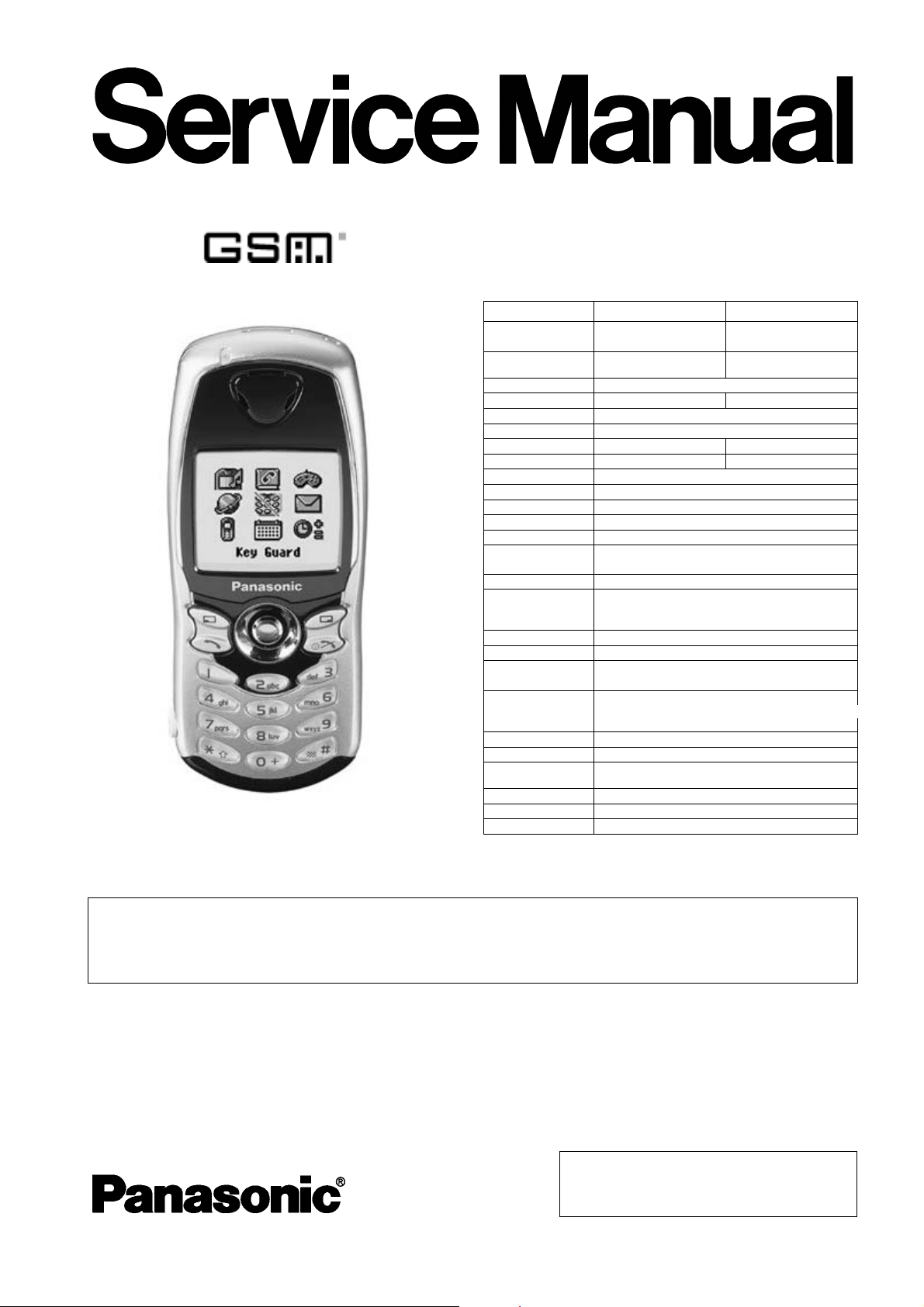
Digital Cellular Phone
EB-GD67
Order Number: MMCD020801C8
900 MHz
Frequency Range Tx: 880 - 915MHz Tx: 1710 -1785 MHz
Tx/Rx frequency
separation
RF Channel Bandwidth 200 kHz
Number of RF channels 174 374
Speech coding Full rate/Half rate/Enhanced Full rate
Operating temperature -10 °C to +55 °C
Type Class 4 Handheld Class 1 Handheld
RF Output Power 2 W maximum 1 W maximum
Modulation GMSK (BT = 0.3)
Connection 8 ch / TDMA
Voice digitizing 13 kbps RPE-LTP / 13 kps ACLEP / 5.6 kps CELP / VSLEP
Transmission speed 270.833 kbps
Signal Reception Direct conversion
Antenna Impedance 50 Ω
(External Connector)
Antenna VSWR < 2.1 : 1
Dimensions Height: 109 mm
Vol ume 81 c c
Weight 81 g
Display Graphical chip on glass liquid crystal, Alphanumeric,
Illumination
Keys 16-key Keypad, Navigation key.
SIM
External DC Supply
Vol tage
Battery 3.7 V nominal, 690mAh, Li-Ion
Standby Time 60 - 190 hrs
Talk Time 1.5 - 6.5 hrs
Talk and standby time will be dependent on network conditions, SIM card, backlight usage
and network condition.
Rx: 925 - 960 MHz Rx: 1805 -1880 MHz
45 MHz 95 MHz
Width: 45 mm
Depth: 20 mm
101 x 80 pixels, 256-colour palette (RGB).
8 LEDs for Keypad Backlighting (Green)
1 LED for LCD Backklighting (White)
2 LEDs for Incoming call (Green) and Charging (Red)
3 V Plug-in type only
5.8 V
1800 MHz
WARNING
This service information is designed for experienced repair technicians only and is not designed for use by the general public. It does not
contain warnings or cautions to advise non-technical individuals of potential dangers in attempting to service a product.
Products powered by electricity should be serviced or repaired only by experienced professional technicians. Any attempt to service or
repair the product or products dealt with in this service manual by anyone else could result in serious injury or death.
© 2002 Matsushita Mobile Communications
Development of Europe Ltd. All rights reserved.
Unauthorized copying and distribution is a violation
of law.
Issue 1
Revision 0

COMPANY LIABILITY
Every care has been taken to ensure that the contents of this manual give an accurate representation of the equipment.
However, Matsushita Mobile Communications Development of Europe Ltd. accepts no responsibility for inaccuracies which
may occur and reserves the right to make changes to the specification or design without prior notice.
The information contained in this manual and all rights in any design disclosed therein, are and remain the exclusive property
of Matsushita Mobile Communications Development of Europe Ltd.
Other patents applying to material contained in this publication:
CP8 PAT E N T S
Comments or correspondence concerning this manual should be addressed to:
Matsushita Mobile Communications Development of Europe Ltd.,
2 Gables Way
Thatcham,
Berkshire.
RG19 4ZB.
ENGLAND
CONTENTS
Page Page
1 INTRODUCTION 1
1.1 Purpose of this Manual 1
1.2 Structure of the Manual 1
1.3 Servicing Responsibilities 1
2 GENERAL DESCRIPTION 2
2.1 General 2
2.2 Features 2
2.3 Telephone Handset Main Kit 2
3 OPERATING INSTRUCTIONS 3
3.1 General 3
3.2 Liquid Crystal Display 3
3.3 Location of Controls 4
3.4 Concept of Operation 5
3.5 Alpha Entry 5
3.6 Features Menu Structure 6
4 TECHNICAL DESCRIPTION 7
4.1 RF Overview 7
4.2 Transmitter 8
4.3 Receiver 9
4.4 Baseband Overview 10
4.5 Power Supplies 14
5 DISASSEMBLY / REASSEMBLY 19
5.1 General 19
5.2 Disassembly 20
5.3 Reassembly 23
6 REPAIR PROCEDURES 24
6.1 Introduction 24
6.2 Lead Free (PbF) solder 24
6.3 External Testing 24
6.4 Test Equipment Setup 27
7 INTERFACES AND TEST POINTS 29
7.1 Interfaces 29
7.2 Test Points 32
8 CALIBRATION PROCEDURES 33
8.1 Introduction 33
8.2 Carrier Power Calibration 33
8.3 RSSI 37
8.4 Battery Calibration 38
9 REPLACEMENT PARTS LIST 40
9.1 Case and Cover Parts 40
9.2 Sub-Assemblies 41
9.3 PCB Variants 42
9.4 PCB Components 42
9.5 Refurbishment Kits 44
9.6 Jigs and Tools 44
9.7 Document Packs 45
10 CIRCUIT DIAGRAMS 47
11 LAYOUT DIAGRAMS 53
Issue 1 – ii – MMCD020801C8
Revision 0 Service Manual

INTRODUCTION
1 INTRODUCTION
WARNING
The equipment described in this manual contains polarised capacitors utilising liquid electrolyte. These devices are entirely safe provided
that neither a short-circuit or a reverse polarity connection is made across the capacitor terminals. FAILURE TO OBSERVE THIS
WARNING COULD RESULT IN DAMAGE TO THE EQUIPMENT OR, AT WORST, POSSIBLE INJURY TO PERSONNEL RESULTING
FROM ELECTRIC SHOCK OR THE AFFECTED CAPACITOR EXPLODING. EXTREME CARE MUST BE EXERCISED AT ALL TIMES
WHEN HANDLING THESE DEVICES.
Caution
The equipment described in this manual contains devices sensitive to electrostatic discharge (ESD). Damage can occur to these devices
if the handling procedures described in Section 4 are not adhered to.
Caution
This equipment contains an internal battery in addition to the external battery packs. These batteries are recyclable and should be
disposed of in accordance with local legislation. They must not be incinerated, or disposed of as ordinary rubbish.
Caution
The equipment uses a Printed Circuit Board PCB manufactured using Lead Free (PbF) solder. The procedures described in Section 6
should be adhered to when repairing these items.
1.1. Purpose of this Manual
This Service Manual contains the information and procedures required for installing, operating and servicing the Panasonic
GSM Personal Cellular Mobile Telephone system operating on GSM Digital Cellular Networks.
1.2. Structure of the Manual
The manual is structured to provide service engineering personnel with the following information and procedures:
1. General and technical information - provides a basic understanding of the equipment, kits and options, together with
detailed information for each of the major component parts.
2. Installation and operating information - provides instructions for unpacking, installing and operating the equipment.
3. Servicing information - provides complete instructions for the testing, disassembly, repair and reassembly of each major
component part. Step-by-step troubleshooting information is given to enable the isolation and identification of a
malfunction, and thus determine what corrective action should be taken. The test information enables verification of the
integrity of the equipment after any remedial action has been carried out.
4. Illustrated parts list - provided to enable the identification of all equipment components, for the ordering of spare /
replacement parts.
1.3. Servicing Responsibilities
The procedures described in this manual must be performed by qualified service engineering personnel, at an authorised
service centre.
The service engineering personnel are responsible for fault diagnosis and repair of all equipment described in this manual.
MMCD020801C8 Section 1 Issue 1
Service Manual – 1 – Revision 0
GENERAL DESCRIPTION
2 GENERAL DESCRIPTION
2.1. General
This section provides a general description and kit composition details for the Digital Cellular Phone and optional kits.
2.2. Features
The Panasonic Phone Model GD67 is a high performance, small, light, telephone handset for business and domestic use on
General Packet Radio Service (GPRS) running on GSM networks. The following features are provided:
• Triple Rate, which includes Full Rate, Half rate and Enhanced Full Rate (EFR) speech, codec.
• Dual Band, E-GSM 900 and GSM 1800 operation.
• GPRS-compatible (Class 8).
• 256-colour Liquid Crystal Display.
• Enhanced Message Service (EMS).
• Tegic T9 Text Entry.
• Voice Ringer.
• Wireless Application Protocol (WAP) Browser.
• Backup Battery.
• 16-voice polyphonic ringtones.
• Downloadable polyphonic melody ring tones.
• Clock, Calculator and Currency Converter.
• Changeable Inlay Card for Case Back.
2.3. Telephone Handset Main Kit
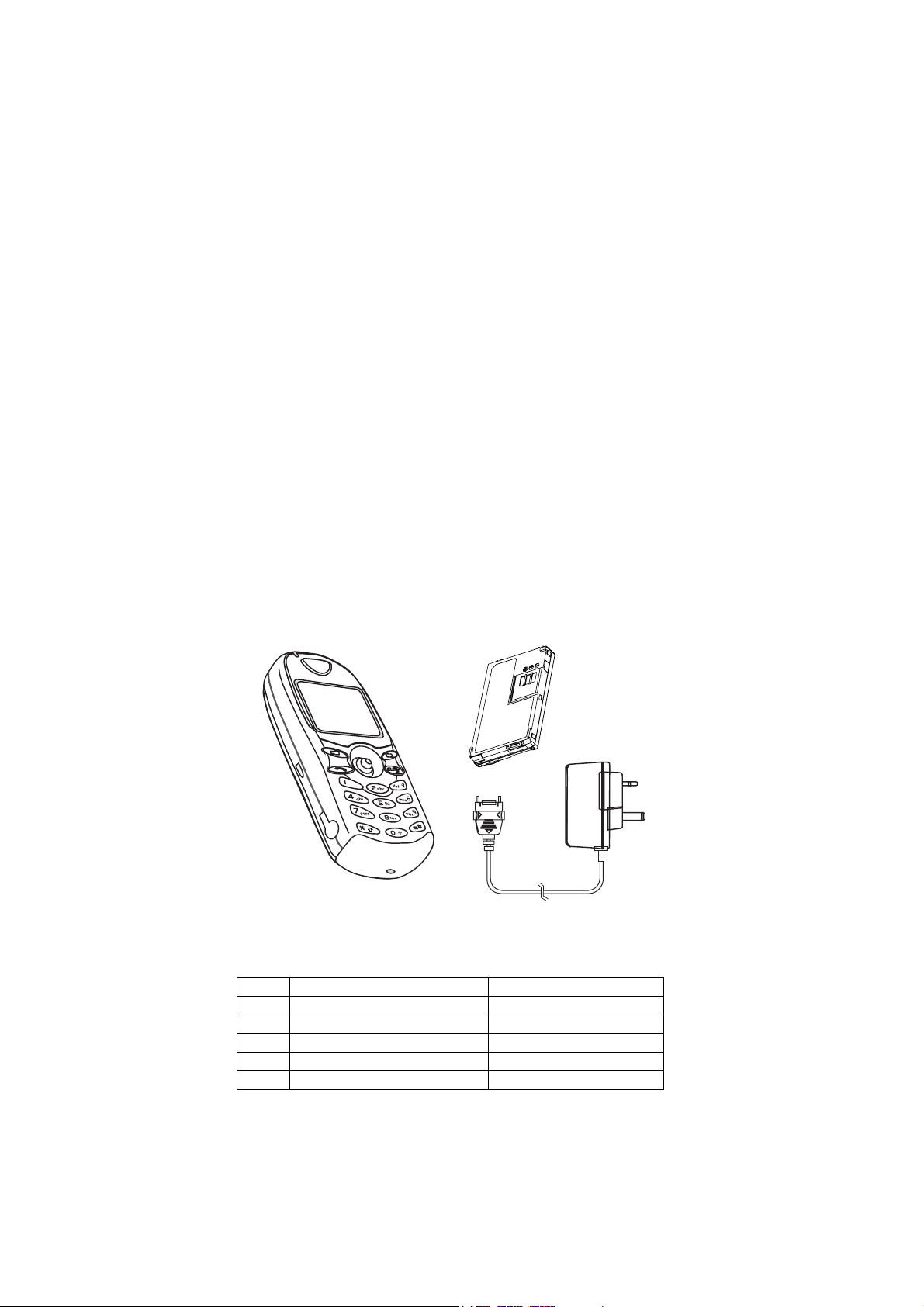
1
Figure 2.1: Telephone Handset Main Unit Kit Contents
ITEM DESCRIPTION PART NUMBER
1 Main Unit EB-GD67
2 Battery, Standard EB-BSD67
3 Travel Charger EB-CAD95
- Inlay Card Template See Section 9
- Document Pack See Section 9.
2
3
10595-1
Issue 1 Section 2 MMCD020801C8
Revision 0 – 2 – Service Manual
OPERATING INSTRUCTIONS
3 OPERATING INSTRUCTIONS
3.1. General
This section provides a brief guide to the operation and facilities available on the telephone handset. Refer to the Operating
Instructions supplied with the telephone for full operational information.
3.2. Liquid Crystal Display
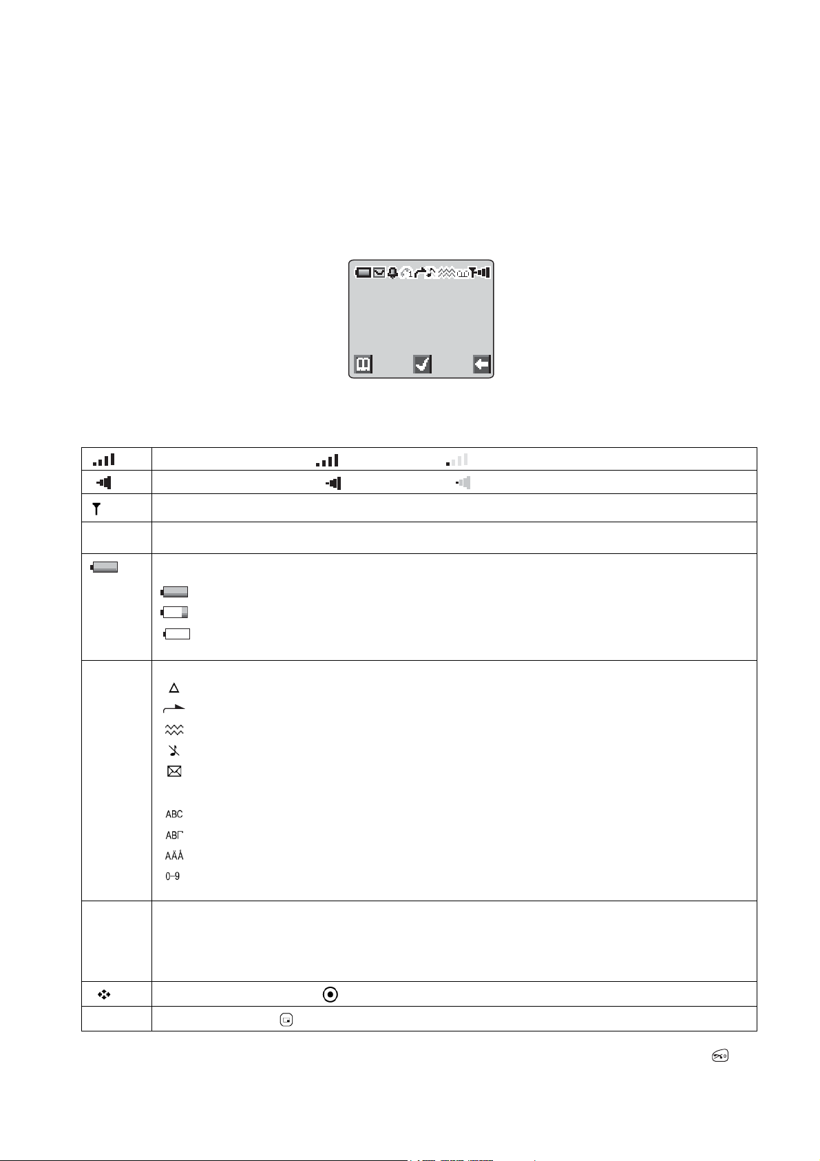
The telephone handset has a graphical chip on glass display.
10580-1
Figure 3.1: Liquid Crystal Display
The following icons are available:
Indicates GSM signal strength: strong signal area; weak signal area.
Indicates GPRS signal strength: strong signal area; weak signal area.
Indicates that it is possible to make an emergency call.
Menu
Number
Menu Icon Displays a small icon related to the current status of the telephone:
Information
Icon
The number of the feature indicated by the pointer. To access a feature enter the menu number on the keypad.
Displays the battery charge level:
Battery is at full charge
Battery requires charging.
The battery icon scrolls during charging.
telephone is roaming on a non-home network.
using the “Call Divert” feature or the telephone has Call-Divert set;
shows that vibration alert is switched on;
shows that the telephone is in silent mode.
flashes to indicate that there are unread text (SMS) messages. Lit when SMS area is full;
indicates the telephone is locked;
O
shows that the normal character set has been selected;
shows that the Greek character set has been selected;
shows that the Extended character set has been selected;
shows that numbers have been selected for text entry
T9 indicates that Tegic T9® predictive text mode is selected.
Displays a small icon according to the current menu level:
indicates the alarm is set.
?
indicates the current Phonebook is sourced from the Mobile Phonebook.
>
indicates the current Phonebook is sourced from the SIM Phonebook.
<
Indicates that the navigation key ( ) can be pressed. Each arrow will light individually to indicate which direction is valid.
Option Area
Following some operations, the display will clear automatically after three seconds or after pressing any key except .
Pressing the select key ( ) will select the option displayed in the option area of the display.
-
MMCD020801C8 Section 3 Issue 1
Service Manual – 3 – Revision 0
OPERATING INSTRUCTIONS
3.3. Location of Controls
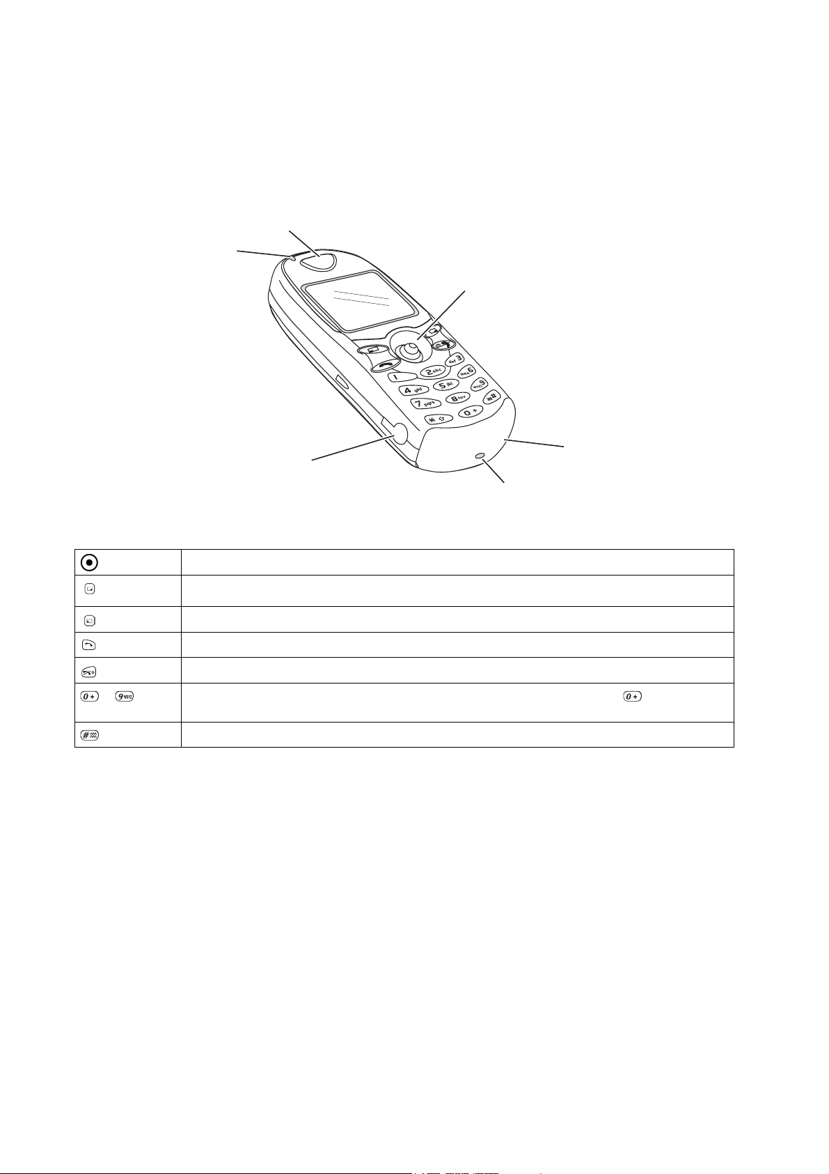
Incoming / Charge indicator:
Green - Incoming call.
Red - Charging battery pack.
External connector:
Used to connect to external accessories or to charging equipment.
EARPIECE
INCOMING CALL /
CHARGE INDICATOR
EARPHONE /
MICROPHONE SOCKET
10594-1
Figure 3.2: Location of Controls
NAVIGATION KEY
MICROPHONE
COVER (EXTERNAL
CONNECTOR)
Navigation Key. Scrolls through options or features menu and increases or decreases volume.
Cancel Key. Used mainly to cancel the current operation and return to the previous menu level. In some menus
it has other functions.
Option key. Primarily used for accessing the Phonebook or switching character types.
,
-
to Digit keys. Enter wild numbers or pauses when pressed and held. Where appropriate the key scrolls up or
'
Send Key. Makes a call.
End Key. Ends a call or switches the telephone on/off when pressed and held.
down through abbreviated control names and then select to reveal the international access code “+”.
Vibrate enable/disable Key. Press and hold to enable or disable the vibrate alert.
Issue 1 Section 3 MMCD020801C8
Revision 0 – 4 – Service Manual
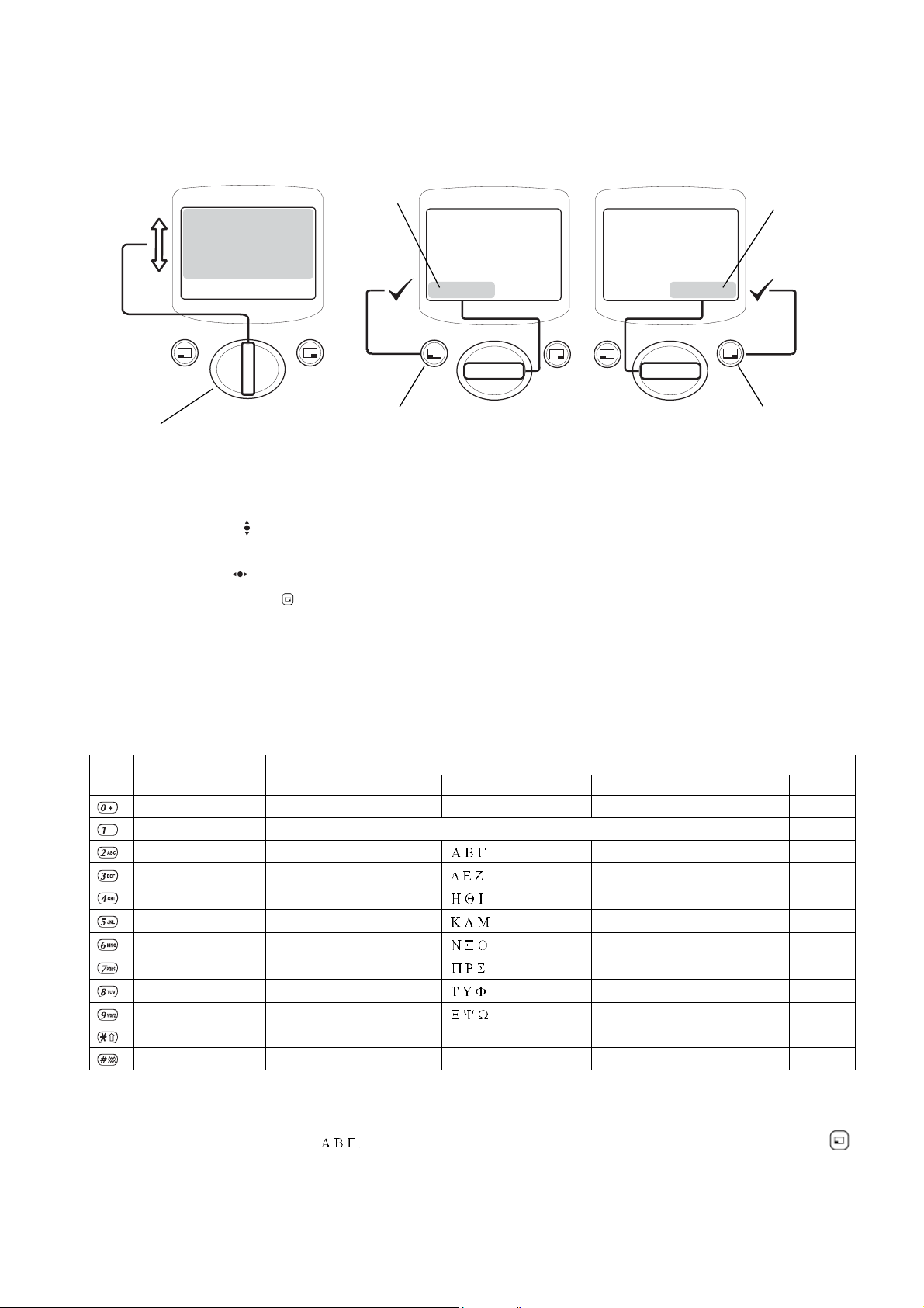
3.4. Concept of Operation
1
There is a close relationship between the Select keys, Navigation key and display.
OPERATING INSTRUCTIONS
SECONDARY
OPTION AREA
SELECT KEY
NAVIGATION
KEY
MAIN
OPTION AREA
SELECT KEY
10626-
Figure 3.3: Concept of Operation
Pressing up and down ( ) will move the pointer up and down and scroll through more information in the main area of the
display.
Pressing left and right ( ) will scroll through options in both option areas of the display. To choose the required option, press
the corresponding Select Key ( ).
3.5. Alpha Entry
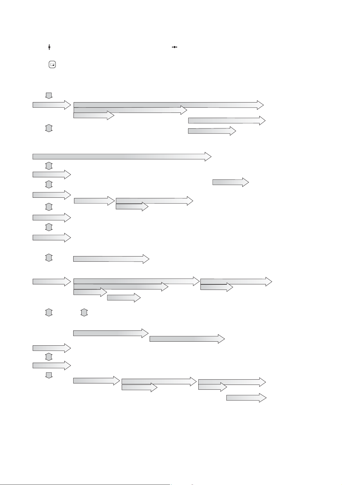
3.5.1 Character Set / Key Assignments
Alpha entry is used to enter alphanumeric characters in to the Phonebook, Short Messages and Greeting Message areas
Key
Alternatives + - + - + - 0+P_
Punctuation “ @ – , . ; : ! ¡ ? ¿ ( ) ‘ & % + – / < > = £ $ ¥ ¤ § 1
abc A B C a b c A Ä Å Æ B C Ç a à b c 2
def D E F d e f D E É F d e è é f 3
!
ghi G H I g h i G H I g h i ì 4
"
jkl J K L j k l J K L j k l 5
#
mno M N O m n o M N Ñ O Ö ø m n ñ o ò ö 6
$
pqrs P Q R S p q r s P Q R S p q r s ß 7
%
tuv T U V t u v T U Ü V t u ù ü v 8
&
wxyz W X Y Z w x y z W X Y Z w x y z 9
'
Shift / Lock * * * *
*
Space # # # #
T9® Normal Greek Extended Numeric
Each time a key is pressed, it will display the next character. When another key is pressed, or no key is pressed for a short
time, the cursor will move to the next position.
To cycle between Greek characters ( ), extended characters (W), numerals (X) and normal characters (U) press .
Character / Operation
MMCD020801C8 Section 3 Issue 1
Service Manual – 5 – Revision 0
OPERATING INSTRUCTIONS
3.5.2 Editing Alpha Entry
Pressing will move the cursor up or down one line. Pressing will move the cursor left or right one character. When the
cursor is moved over a character and another key pressed this will insert the new character.
Pressing will delete the character to the left of the cursor.
3.6. Features Menu Structure
1. Personalise
2. Phonebook
3. Games
4. Browser
5. Key Guard
6. Messages
Language
Tones
Display Setting
Quiet Mode
Media Folders
Auto Answer
DTMF Length
Defaults
Game 1
Game 2
Settings
Start Browser
Browser Setting
Inbox
Outbox
Create
Chat SMS
Parameters
Idle Screen
Colour Themes
Greeting
Animation
Contrast
Backlight Time
Linger Time
Server Setting
< Server 1 >
< Server 2 >
Recipient Group
Auto Delete
Message Centre
All Tones
Ring Volume
Ring Type
Melody Composer
Voice Ringer
Key Volume
Key Tone Type
Warning Tone
Browse
Create
Voice Command
Alert Profile
Group Setting
Review
My Numbers
Voicemail
GSM
GPRS
Hot Key Dial
Recording
Playback
SIM Phonebook
Mobile Phonebook
Display Language
Tegic Language
Voice Calls
Fax Calls
Data Calls
Messages
Voicemail
7.Phone Option
8. Scheduler
9. Applications
Call Service
Call Divert
Security
Network
Games
Voice Memo
Download Melody *
Clock Function
Calculator
Currency
Download Data
Voice Calls
Phone Lock
Call Bar
PIN
PIN2
Fixed Dial
Barred Dial
Clock Set
Clock Format
Alarm Set
Power On Time
Power Off Time
Bar Voice
Bar Fax
Bar Data
Cancel All
Status
Password
New Network
Search Mode
Network List
Fax Calls
Data Calls
Cancel All
Status
Display Pattern
Display Format
Figure 3.4: Features Menu Structure
Calls
Connections
Home
Second
Last Call
Last Connection
All Connections
Call Priority
Automatic
Manual
Time Difference
Summer Time
Auto Adjustment
* Feature is SIM / Network dependent.
All Calls
Caller’s ID
Time Set
Summer Time
Auto Adjustment
Home Country
10600-1
Issue 1 Section 3 MMCD020801C8
Revision 0 – 6 – Service Manual

TECHNICAL DESCRIPTION
4 TECHNICAL DESCRIPTION
4.1. RF Overview
4.1.1 General Specifications
The telephone is a Dual Band product incorporating two switchable transceivers, one for the E-GSM 900 band and another for
the GSM 1800 (DCS 1800) band. The transmit and receive bands for the mobile are given in the table below:
Tx Rx
E-GSM 900 880-915 MHz 925-960 MHz
GSM 1800 1710-1785 MHz 1805-1880 MHz
Other notable technical features are as follows:
E-GSM 900 GSM 1800
Rx Bandwidth 35 MHz 75 MHz
Tx Bandwidth 35 MHz 75 MHz
Duplex Spacing 45 MHz 95 MHz
Number of Channels 174 374
AFRCN (Channel Numbers) 0-124 512-885
975 - 1023
1st Tx Channel 880.2 MHz 1710.2 MHz
(Ch 975) (Ch 512)
Last Tx Channel 914.8 MHz 1784.8 MHz
(Ch 124) (Ch 885)
1st Rx Channel 925.2 MHz 1805.2 MHz
(Ch 975) (Ch 512)
Last Rx Channel 959.8 MHz 1879.8 MHz
(Ch 124) (Ch 885)
Maximum Tx Power 33.0 dBm 30.0 dBm
(Class 4) (PL5) (Class 1) (PL0)
Minimum Tx Power 5.0 dBm 0.0 dBm
(PL19) (PL15)
4.1.2 Main PCB Description
All RF components are located on one side of the top half area of the PCB, with the baseband components (Logic circuits)
occupying the lower half of the PCB. The RF circuit area is shielded by two metal screens and the Logic circuits area by one
screen.
The LCD Module and keypad are mounted on the reverse side of the PCB.
MMCD020801C8 Section 4 Issue 1
Service Manual – 7 – Revision 0
TECHNICAL DESCRIPTION
4.2. Transmitter
4.2.1 Functional Description
U200
RF
VCO
÷4
I
Q
÷2
I
Q
DUAL BAND
TRANSCEIVER (PART)
U205
BUFFER AMP
EGSM 900
GSM 1800
FL201
SAW
FILTER
ATTENUATOR
x2
U203
DUAL BAND
PA
EGSM 900
GSM 1800
U202
APC
E100
E101
S201
SWITCH
MODULE
ANTENNA
RF TP /
SWITCH
10577-1
Figure 4.1: Transmitter Block Diagram
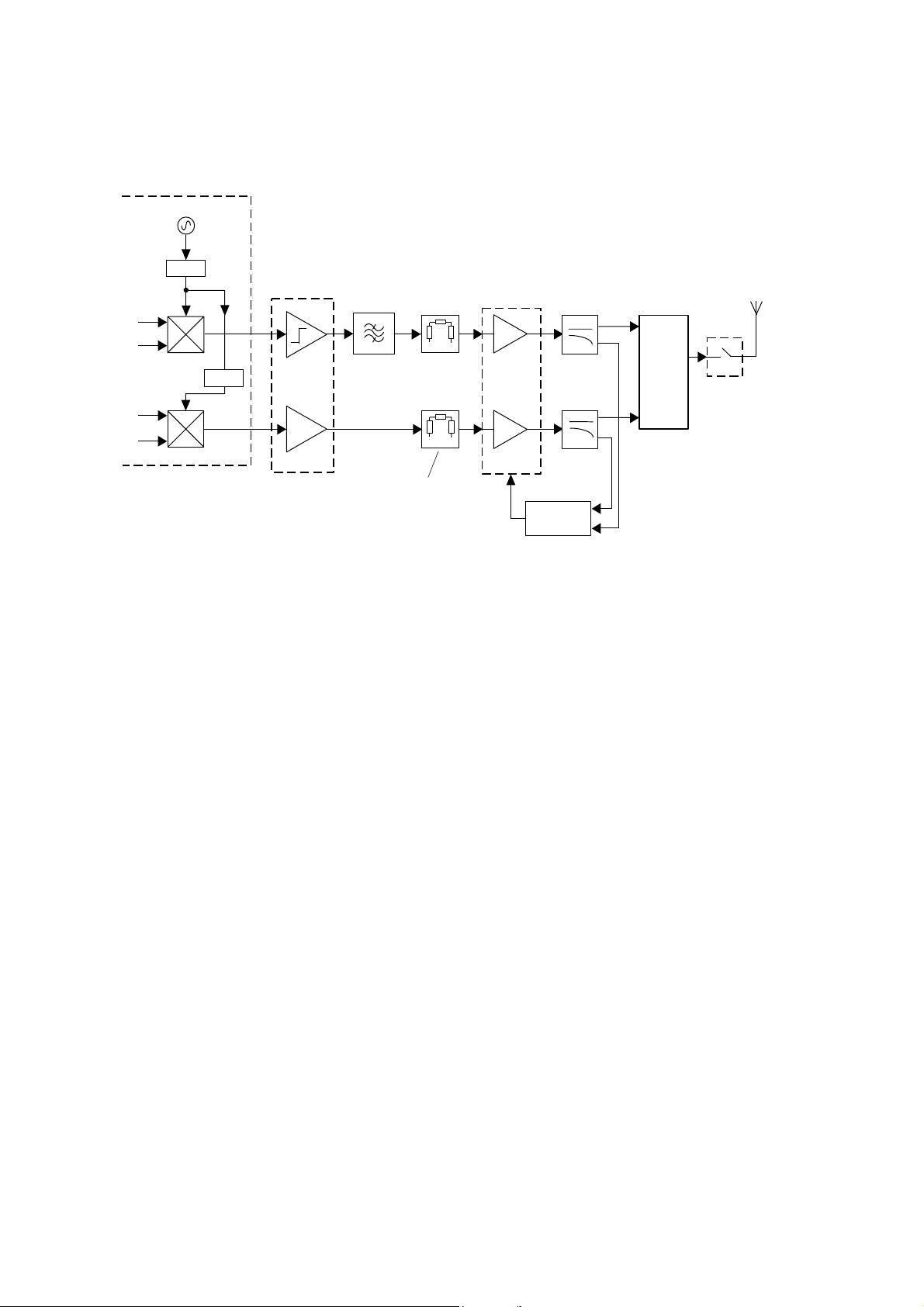
The transmitter design is based on an IQ Modulator and operates at Class 4 (2W) in the GSM 900 band and at Class 1 (1W)
in the GSM 1800 band. The architecture has been carefully chosen to limit GSM transmitter noise in the receiver band without
the requirement for a duplexer.
A dual band transceiver IC (U200) provides the following transmitter functions:
I, Q Quadrature modulator
Down conversion mixer for modulated signal to intermediate frequency.
Phase detector for PLL modulation loop.
The modulator output is fed into dual band buffer amplifier U205 which ensures temperature stability and AM suppression. A
three port EGSM SAW filter FL201 filters EGSM 900 output to provide extra filtering against transmitter noise in the receiver
band. The selected transmitter band (EGSM 900 or GSM 1800) output signal from U205 is then attenuated and applied to its
dedicated input of the dual band Power Amplifier (PA) U203.
Filtering of the transmitter harmonics, most of which are from the PA, is provided by couplers E100 (EGSM 900) and E101
(GSM 1800). The output from the couplers is applied to the antenna switch S201 which provides a connection path to the RF
test point CN201 and the internal antenna.
The coupled outputs are combined at the input of U202, an Automatic Power Control (APC) IC, to control the gain and output
power of the PA. An RF detector in U202 produces a baseband output which is compared with a control signal from the logic
section to produce a control signal for the PA.
Issue 1 Section 4 MMCD020801C8
Revision 0 – 8 – Service Manual
4.3. Receiver
4.3.1 Functional Description
TECHNICAL DESCRIPTION
FL203
Rx SAW
FILTERS
EGSM 900
GSM 1800
LNA
RF
LO
LNA
U200
DUAL BAND TRANSCEIVER
BASEBAND
FILTERS
PGC
AMP
IR
IRX
BASEBAND
AMPLIFIERS
QR
QRX
10576-1
RF
TEST
S201
SWITCH
MODULE
LPF
Rx
Tx
Tx
Rx
HPF
Figure 4.2: Receiver Block Diagram
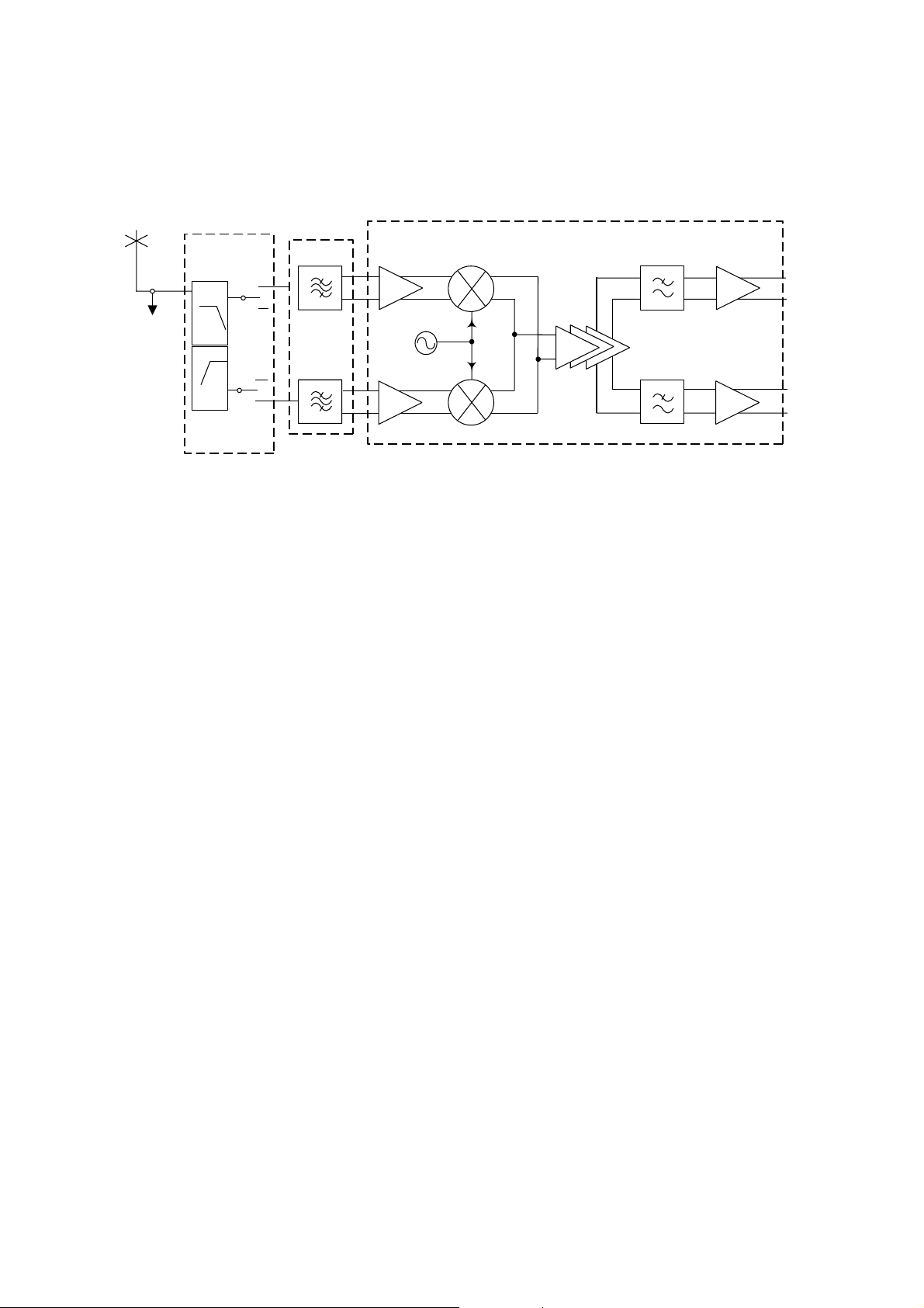
The main building block for the receiver is the dual band transceiver IC (U200) which includes a direct conversion receiver
with I and Q quadrature demodulation.
Received signals from the antenna are passed to the dual band antenna switch module S201. This module contains a
diplexer which filters the signal to the required receiver path (E-GSM 900 or GSM 1800). Pin diode switches within S201 route
the signal path from the transmitter or to the receiver as required. Output signals from S201 are then applied via the dual band
SAW filter FL203 and impedance matching circuits to the balanced Low Noise Amplifiers (LNA) onboard U200.
Output from the LNAs is then converted directly to baseband frequency by a quadrature demodulator mixer. The local
oscillator (LO) signal presented to the mixer is provided by an internal VCO and divided by four. The VCO operates over the
frequency range 3700.8 MHz - 3839.2 MHz.
At baseband, the GSM signal is passed through a 1-pole blocking filter (comprising two external capacitors) and a channel
filter. These filters provide some attenuation to adjacent channel signals at the receiver input, e.g. ±200 kHz, ±400 kHz and
±600 kHz.
These filters are designed to give low group delay ripple, typically 1µs maximum over the temperature range specified for
U200, across the GSMK modulation baseband (80 kHz at baseband). An internal equaliser stage is used to correct any group
delay variation which causes distortion of the received signal.
The baseband signal is then amplified by nine programmable variable gain amplifier stages within U200 which provide gain
settings between -20 dB and +58 dB. The LNA can be programmed to switch on or off, providing a further step gain of 20 dB.
The I and Q baseband signals are then offset to 1.35 V DC produced internally by U200. This offset level provides the largest
dynamic range available for the receiver, which is limited by IOTA. IOTA provides A to D conversion of the GSM signal and a
further 45 dB attenuation of adjacent channel signals through DSP filtering.
MMCD020801C8 Section 4 Issue 1
Service Manual – 9 – Revision 0
TECHNICAL DESCRIPTION
4.4. Baseband Overview
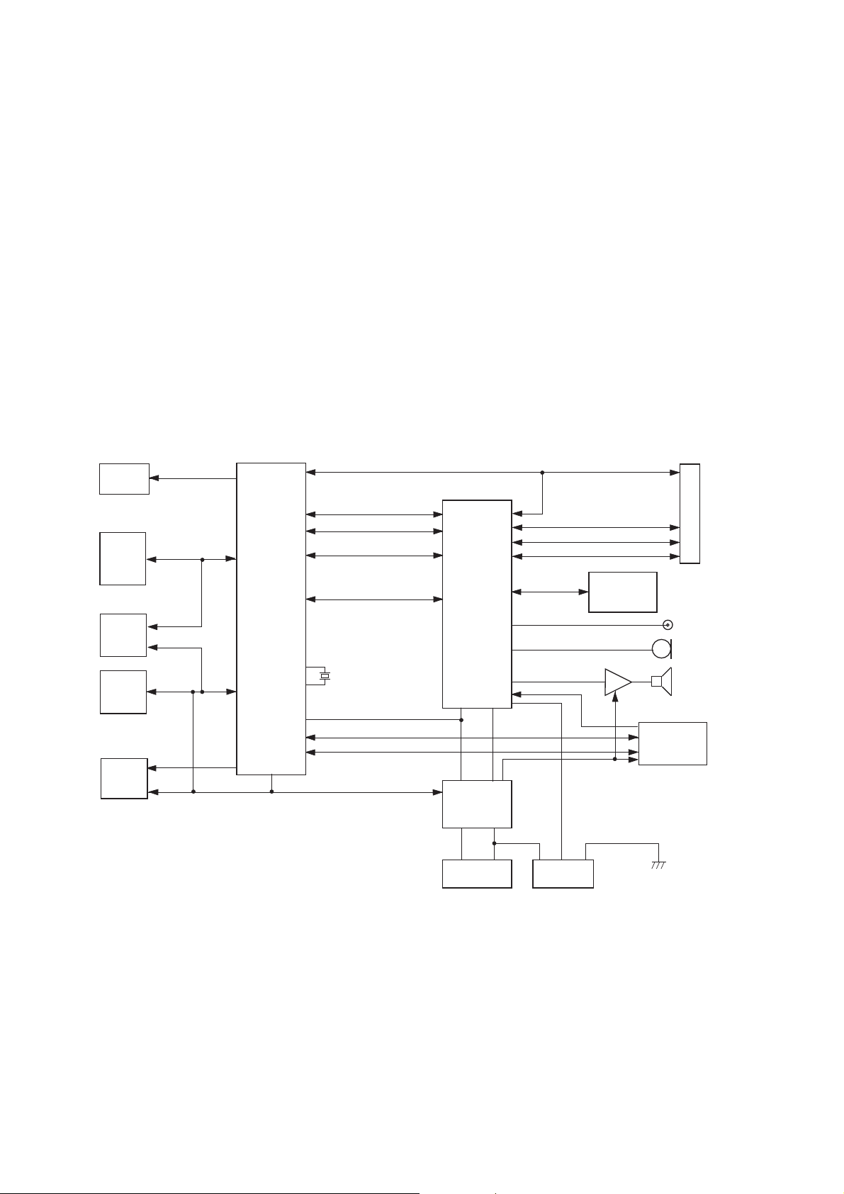
4.4.1 Introduction
The Baseband circuits of the phone are required to perform the following functions:
• Equalisation
• Channel coding / decoding
• Speech coding / decoding
• Data Encryption
• Layer 1, 2 and 3 software tasks
• Man Machine interface (MMI)
• System Interface
• SIM Interface and Management
• Audio and Tone Generation
• Power supply and battery management
• RF power control
• Synchronisation
• Real time clock
VIBRATE
MOTOR
U640
FLASH
+
SRAM
LCD
KEYPAD
BACK-
LIGHTS
CS0, CS1
CS3
U600
CALYPSO
RF DIGITAL CONTROL LINES
U620
BASEBAND INTERFACE
VOICEBAND INTERFACE
MCU INTERFACE
SIM INTERFACE
IOTA
RTC
(32 kHz)
uWIRE I/F
INT1,INT2
DISCRETE
ACCESSORY
INTERFACE
I/O
CONNECTOR
Figure 4.3: Baseband Block Diagram
I AND Q LINES
POWER RAMP SIGNAL
AFC
SIM CARD
+ T -
BATTERY
U750
RF
I/F
PERSONAL
HANDSFREE
MIC
SPEAKER
U751
MELODY
GENERATOR
10566-1
The GD67 Baseband is built around a GSM chipset developed by Texas Instruments. The chipset comprises two chips,
CALYPSO and IOTA. The highly integrated nature of the chips means that each contain a large number of functions.
CALYPSO is a signal processing device with DSP and CPU. The DSP performs channel and speech encoder/decoder tasks,
together with equalisation and encryption. The CPU runs layer 1, 2, and 3 software, controls the MMI, SIM and system
interfaces, real time clock, and battery and power management. CALYPSO also controls IOTA.
IOTA provides frame timing, A/D conversion, RF power control, audio interfacing including tone generation, and baseband
power supplies.
Issue 1 Section 4 MMCD020801C8
Revision 0 – 10 – Service Manual
TECHNICAL DESCRIPTION
4.4.2 Keypad
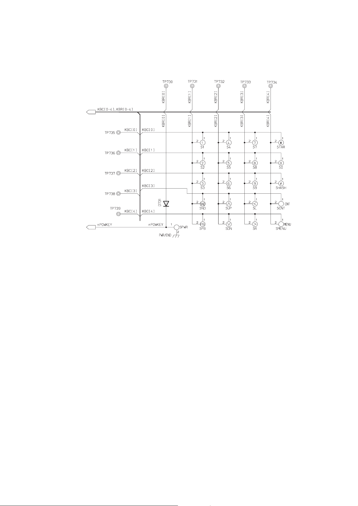
The Keypad has a 5 x 5 matrix, allowing 25 keys to be scanned. When a key being pressed, a keypad interrupt is generated.
To find which key has been pressed, the software scans each column in turn and reads which row is active. Because of key
bounce, the key press is confirmed twice at approximately 20 ms intervals.
U600
CALYPSO
U620
IOTA
10571-1
Figure 4.4: Keypad Connections
As the End Key doubles for the ON / OFF key, it is allocated an entire row of the keyboard scan.
Keyboard scanning is controlled by software. ‘Key pressed’ is indicated by an interrupt, but ‘key released’ is monitored by
software.
4.4.3 Subscriber Identity Module (SIM)
The SIM interface is designed to support 3 V SIMs. As CALYPSO operates from a 2.8 V supply, level translation from 3 V is
provided by IOTA.
MMCD020801C8 Section 4 Issue 1
Service Manual – 11 – Revision 0
TECHNICAL DESCRIPTION
4.4.4 TPU
The TPU provides the GSM TPU TDMA timing requirements for the system.
TPU Timing output signal assignments of CALYPSO
Name Ball No. Function Connection Configuration
TSPACT 0 M12 PAON External Used for triggering Measuring Equipment
TSPACT 1 M14 PLLON RF
TSPACT 2 L12 NC N/A
TSPACT 3 L13 NC RF
TSPACT 4 J10 TX_ON1 RF
TSPACT 5 K11 NC N/A
TSPACT 6 K13 DCS_PAON RF
TSPACT 7:CLKX_SPI K12 GSM_PAON RF
TSPACT 8:nMREQ K14 NC N/A
TSPACT 9:MAS1 J11 NC N/A
TSPACT 10:nWAIT J12 nWAIT LCD Used with RnW
TSPACT 11:MCLK J13 NC N/A
4.4.5 CPU Memory
To reduce component space, the phone memory consists of 64 MB Flash and 8 MB SRAM MCP. Additionally, CALYPSO has
4 MB internal SRAM, thus extending total SRAM to 12MB.
4.4.6 LCD
The LCD module is of a chip on flex (COF) construction.
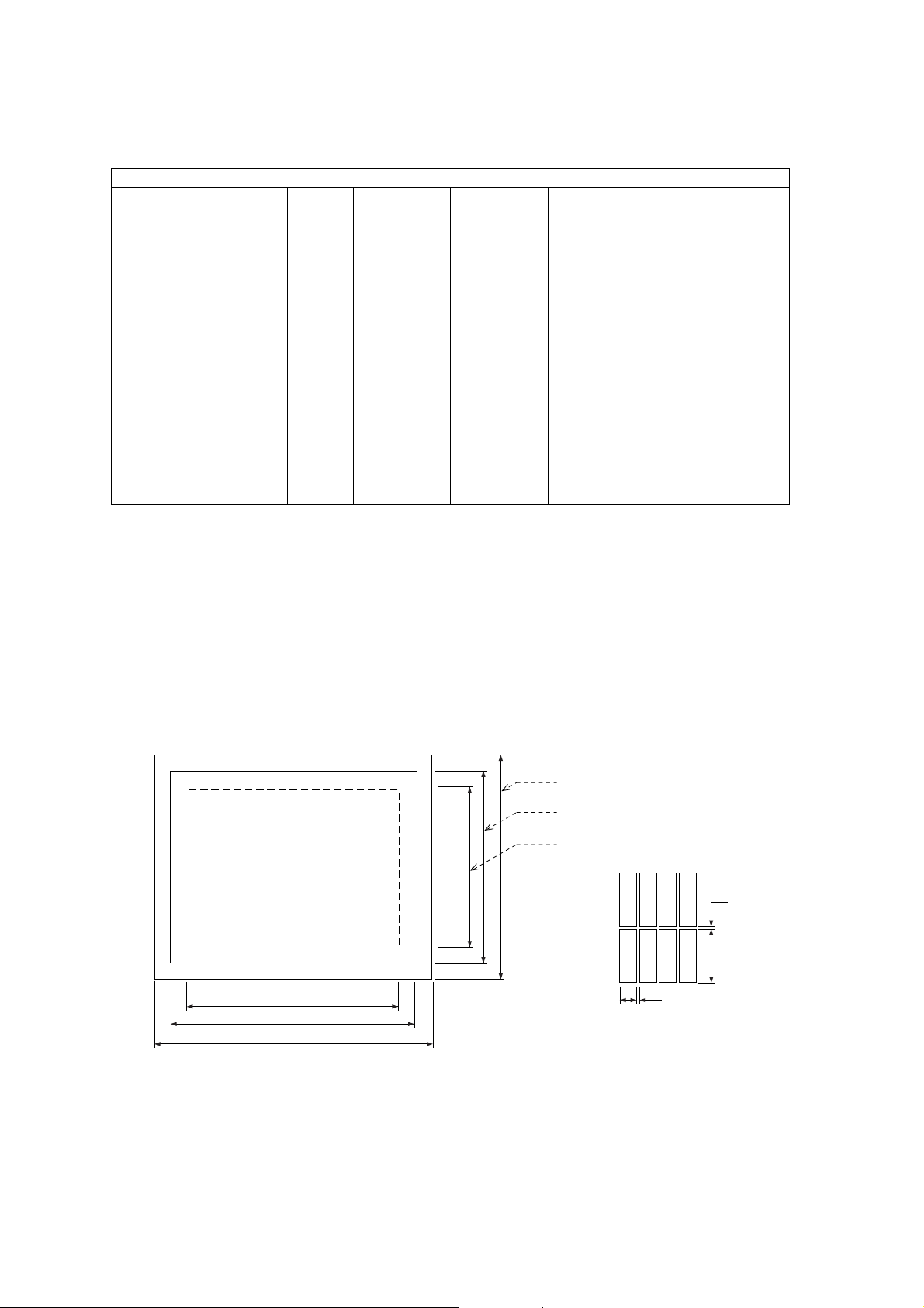
The display has 101 x 80 pixels, each capable of displaying 256 colours. There is a one-to-one relationship between the
internal Graphics RAM (GRAM) and each pixel.
Glass Size
Viewable Area
Active Area
101 x 80 Pixels
(GD67)
29.38
32.40
35.6
Dimensions are in millimetres (mm)
34.20
28.90
25.27
R
R
0.087
G
B
R
G
B
R
0.01
0.01
0.306
10567-1
Figure 4.5: LCD Dimensions
The LCD driver is controlled by setting the command register through the CALYPSO u-wire interface and an I/O line which
distinguishes between command or data. To send data or a command to the display driver, the nSCS0 line is used for chip
select. LCD_CD (I/03) is set high to send data and set low to send commands.
Issue 1 Section 4 MMCD020801C8
Revision 0 – 12 – Service Manual

TECHNICAL DESCRIPTION
4.4.7 Real Time Clock (RTC)
Clock functions are provided by a Real Time Clock built into CALYPSO. The module is synchronised by a 32.768 kHz crystal
and is powered via a dedicated regulator in IOTA and is backed up by a 2.5 V button battery.
CALYPSO has a clock auto compensation function to take into account any inaccuracies of the crystal. It is able to calibrate
crystal tolerance / drift by writing to the compensation registers. This calibration can adjust the clock to a resolution of
1 x 32768 Hz clock period.
Registers for RTC are assigned between $FFFE:1800 - $FFFE:1814.
4.4.8 Timers
There is a watchdog timer and two 16 bit general-purpose timers which can be used either as auto reload or one-shot timers
to provide interrupts to the ARM CPU. The watchdog timer receives a 928 kHz clock signal from the CALYPSO clock module.
A combination of pre-scaler and timer register gives a time range of 1.078 µs to 9.039 s. The general purpose timers receive
a 812.5 kHz clock signal.
4.4.9 UART
CALYPSO has two UART ports, UART modem and UART / IrDA. The UART / modem port is used for optional accessories.
The UART / IrDA port is used for data connection, software debugging, factory testing and software downloading.
UART / MODEM PORT ASSIGNMENT
CALYPSO SIGNAL PIN No. FUNCTION I/O
TX_MODEM B9 UART serial data TX O
RX_MODEM A9 UART serial data RX I
DSR_MODEM D9 UART Data Terminal Ready I
RTS_MODEM E8 UART Clear to Send O
CTS_MODEM C9 UART Request to Send I
Registers for the UARTs are located from $FFFF:5000 to $FFFF:5011 (UART / IrDA) and from $FFFF:5800 to $FFFF:5811
(UART / modem).
4.4.10 Accessory Interface
The phone uses discrete components for the buffering and level shifting at the I/O (Accessory) connector. Interface
connections are protected from short circuit currents up to 4.4 mA and a maximum rise time of 1.1µs.
Connection of an accessory will not power up the phone.
MMCD020801C8 Section 4 Issue 1
Service Manual – 13 – Revision 0
TECHNICAL DESCRIPTION
4.5. Power Supplies
4.5.1 Introduction
MAIN
BATTERY
ACC-PWR
EXTPWR
nACC-SENSE
DATA-MODE0
DATA-MODE1
I/O
CN780
BAT-TEMP
Q781
VBAT
ACC-PWR
UPR
UPR
U620
IOTA
VR
VR
VR
VR
VR
EXT-IRQ
VR
VR
VBACKUP
VRRAM
VRMEM
VRIO
VRABB
A28V
VRBB
RPWON
VRRTC
VRSIM
MICBIAS
HEADSET
MIC
R625
BACKUP
VSDD
CELL
U751
MELODY
GENERATOR
RESPWONZ
CN720
(SIM)
D28VB
D18V
ONOFF
VRTC
Figure 5.1: Power Supply Block Diagram
D621
CALYPSO
INT2
U600
D28VR
D28V
RFEN
TCXOEN
U640
FLASH
+ SRAM
VBAT
U204
REG
SPEAKER
AMP
VSTX
VSRF
10578-1
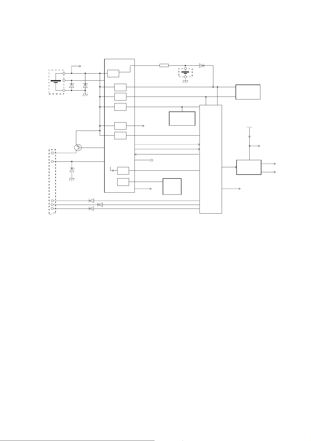
The Power Management Block consists of six parts as follows:
1. Power Source
2. Power On/Off Control
3. Power Source Failure detection
4. Voltage Regulation
5. Battery Charging & Monitoring
6. Accessory Control
4.5.2 Power Source
The battery comprises a single Lithium-Ion (Li-Ion) cell with a nominal voltage of 3.7 V and 690 mAh capacity. This type of
battery has an advantage in weight and size over Nickel Metal Hydride (NiMH) cells.
Issue 1 Section 4 MMCD020801C8
Revision 0 – 14 – Service Manual

TECHNICAL DESCRIPTION
4.5.3 Power On / Off Control
The power on sequence can begin when VBAT >2.6 V or VBACKUP >2.6 V. In this state IOTA (U620) is in Power On
Condition and internal supply UPR is active. RESPWRONZ signal to CALYPSO (U642) is released high.
If IOTA is in the Power On Condition, one of following conditions start the Power Up sequence.
• Power key is pushed for more than 30 ms.
• RPWON input goes high to low for more than 30 ms (e.g. accessory is connected).
• EXTPWR voltage is higher than (VBAT+0.4) V.
• CALYPSO RTC ALARM signal goes high.
The Power Up sequence is as follows:
1. IOTA internal band gap reference is activated.
2. If VBAT < 3.2 V after a timeout of 51.2 ms Power Up sequence is aborted.
3. All regulators (VRDBB, VRMEM, VRRAM, VRIO, VRABB & VRRTC) are enabled.
4. Power Up status bit and internal Reset bits are set.
5. ONNOFF signal is set to activate CALYPSO.
6. ARM in CALYPSO starts running software using 32 kHz clock, and also starts 26 MHz clock.
The following Power Down sequence can only be started by CALYPSO setting the DEVICE_OFF bit in IOTA or, in emergency
case, when VBAT < 2.7 V (or VBAT < Vbackup & VBAT < 2.8 V):
1. If emergency case, INT1 is set low by IOTA.
2. IOTA starts an internal 150 µs watchdog timer to allow CALYPSO to shutdown.
3. ONNOFF signal is reset to deactivate CALYPSO.
4. All regulators (VRDBB, VRMEM, VRRAM, VRIO, VRABB & VRRAM) are disabled.
5. IOTA internal band gap reference is deactivated.
4.5.4 Power Source Detection Failure
The SIM card contains EEPROM. If the power fails (i.e. battery removal) while the SIM is active, the SIM may corrupt its
memory as the supply voltage drops out of specification.
There is sufficient time between Low Voltage Alarm (LVA) detection and IOTA switch-off for the software to cease writing to
the SIM to prevent corruption without the need for any interrupt signal from IOTA.
4.5.5 Voltage Regulation
The voltage regulators for I/O and memories have a nominal output of 2.8 V, and are designed to provide a minimum 2.7 V
output over all load, transients and temperature conditions.
Each power source is specified as follows.
• VRDBB: Power supply for the CALYPSO (Lead Mega Module) LMM block.
Voltage 1.8 V ±0.15 V
Current 120 mA max.
Dropout 100 mV max (load max)
Supply VBAT
This power supply provides the power for CALYPSO internal RAM, ASIC modules, LMM and ARM Blocks, and is
selectable from 1.18 V, 1.4 V and 1.8 V.
• VRIO: Power supply for IOTA ASIC I/O and CALYPSO.
Voltage 2.8 V ±0.15 V
Current 100 mA max.
Dropout 100 mV max (load max)
Supply VBAT
This is the main power supply for the baseband digital sections (I/O and LCD) and some analogue sections. It is also used
for the digital I/O ring on both CALYPSO and IOTA.
MMCD020801C8 Section 4 Issue 1
Service Manual – 15 – Revision 0

TECHNICAL DESCRIPTION
• VRMEM: Power supply used by Baseband Digital part.
Voltage 2.8 V ±0.1 V
Current 60 mA max.
Dropout 100 mV max (load max)
Supply VBAT
Supplies CALYPSO memory interface and external memory components. Selectable between 1.8 V and 2.8 V.
• VRRAM: Power supply for external SRAM.
Voltage 2.8 V ±0.1 V
Current 50 mA max.
Dropout 100 mV max (load max)
Supply VBAT
Supplies the SRAM of U640. When the handset is powered down and the supply is switched off, the external SRAM is
supplied from the backup cell to maintain the contents. This regulator is diode protected from reverse supply.
• VRABB: Digital power supply for IOTA Analogue section.
Voltage 2.8 V ±0.1 V
Current 80 mA max.
Dropout 100 mV max (load max)
Supply VBAT
Supplies power for the IOTA onboard analogue section.
• VRSIM: Digital Power supply for SIM card.
Voltage 1.8 V ±0.15 V
Current 10 µA max.
Dropout 100 mV max (load max)
Supply VBAT
Supplies power for the SIM card. Selectable from 1.8 V an 2.85 V.
• VRTC: Digital power supply for CALYPSO 32 kHz oscillator and RTC module.
Voltage 1.8 V ±0.15 V
Current 10
Dropout 100 mV max (load max)
Supply UPR
Supplies power for the CALYPSO 32 kHz oscillator and RTC module. Selectable from 1.18 V, 1.4 V and 1.8 V. It is
supplied from UPR to enable it to be maintained from the backup cell when the main battery is removed.
µA max.
4.5.6 Regulator Sleep Function
To reduce power consumption in the analogue section of the baseband chipset, the voltage regulators can be placed in a low
power mode or disabled by the processor when it enters a low activity sleep mode. During sleep mode, VRABB is disabled,
and VRDBB, VRIO, VRMEM, VRRAM and VRSIM are switched to low power mode.
Issue 1 Section 4 MMCD020801C8
Revision 0 – 16 – Service Manual
 Loading...