

Panasonic CX-CA1090L Service Manual
General
Power Supply DC 12V (11V - 16V),
Test Voltage 13.2V
Negative Ground
Current Consumption Less than 1.5A
Output Voltage 2.0V (47kΩ//1000pF)
CD Changer
Signal to Noise Ratio More than 85dB (IHF-A)
Channel Separation More than 65dB (IHF-A)
Total Harmonic Distortion Less than 0.05% (30kHz/LPF,
400Hz/HPF)
© 2001 Matsushita Communication Industrial Co.,
Ltd. All rights reserved. Unauthorized copying and
distribution is a violation of law.
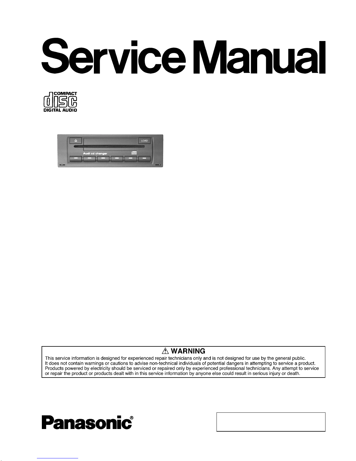
AUDI
CX-CA1090L
6-Disc CD Changer
AUDI No. : 8E0 035 111
VEHICLE : A4
DESTINATION : North America / Europe
PRODUCED AFTER : Oct., 2000 (Europe)
Oct., 2001 (North America)
Dimensions** (W×H×D) 179×52×167mm
Weight** 1.6kg
* Specifications and the design are subject to possible modification
without notice due to improvements.
** Dimensions and Weight shown are approximate.
AUTOMOTIVE ELECTRONICS
Specifications*
ORDER No. AED0104012
I0
1 FEATUERS 2
2 LASER PRODUCTS
2
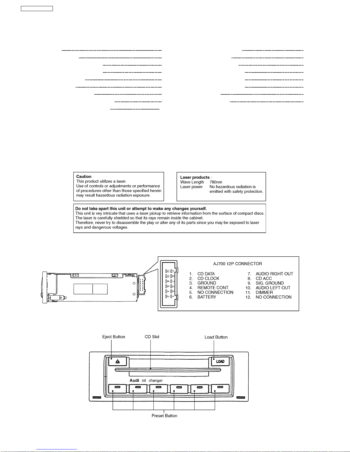
3 REAR VIEW AND CONNECTOR
2
4 FRONT VIEW AND FUNCTIONS
2
5 WIRING CONNECTION
3
6 BLOCK DIAGRAM
4
7 TERMINALS DESCRIPTION
6
8 PACKAGE AND IC BLOCK DIAGRAM
8
9 CD DISC CENTERING ALIGNMENT
11
∙ 6-disc CD changer (in dash board).
∙ Shock Proof Memory.
10 REPLACEM ENT PARTS LIST 12
11 EXPLODE D VIEW (Unit)
14
12 CD CHANGER PARTS LIST
15
13 EXPLODE D VIEW (CD Deck-1)
18
14 EXPLODE D VIEW (CD Deck-2)
19
15 EXPLODE D VIEW (CD Deck-3)
20
16 WIRING DIAGRAM
21
17 SCHEMATIC DIAGRAM
25
∙ Hologram optical pick-up.
∙ Hi-speed disc change.
CONTENTS
Page Page
1 FEATUERS
2 LASER PRODUCTS
3 REAR VIEW AND CONNECTOR
4 FRONT VIEW AND FUNCTIONS
2
AUDI / CX-CA1090L
5 WIRING CONNECTION
3
AUDI / CX-CA1090L
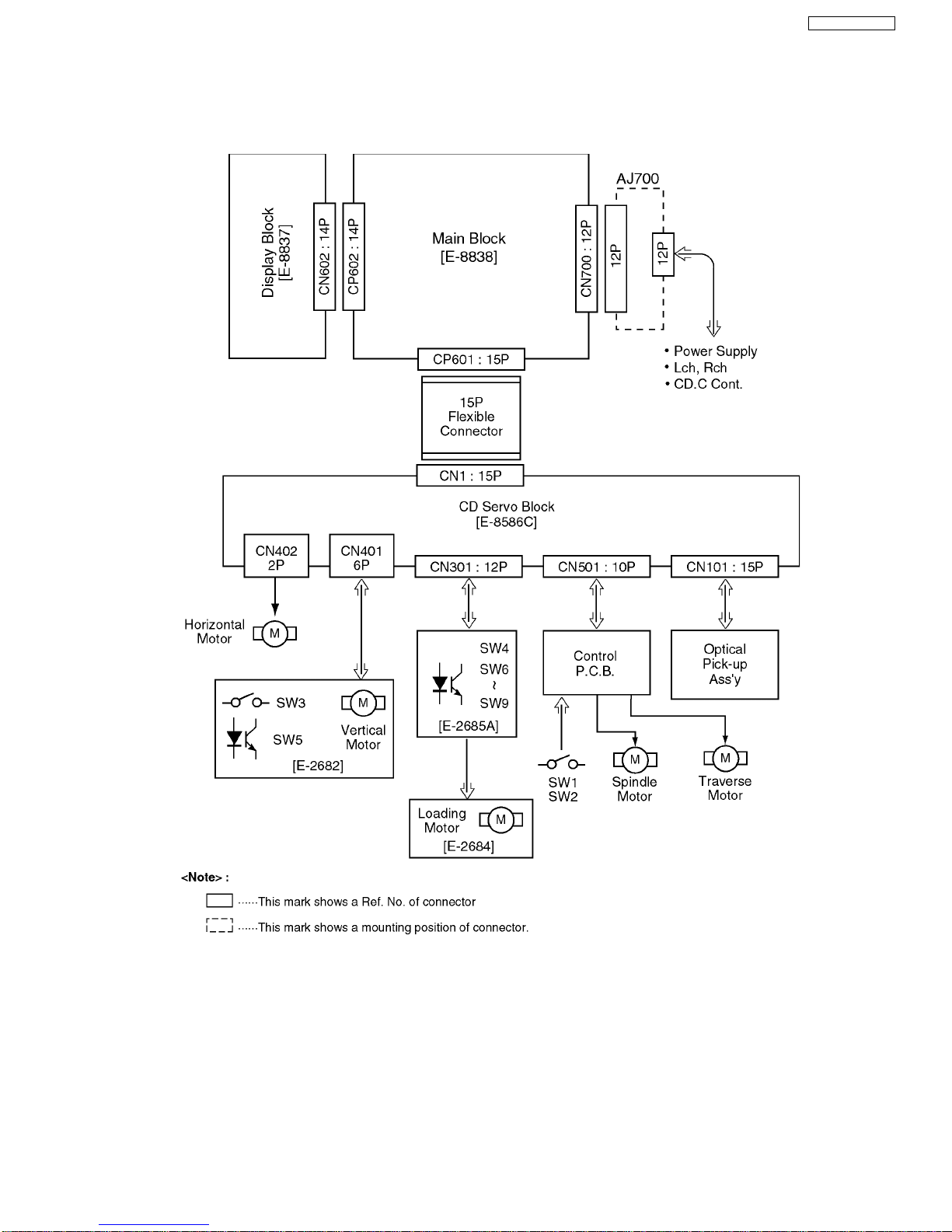
6 BLOCK DIAGRAM
6.1. Main, Display Block
4
AUDI / CX-CA1090L
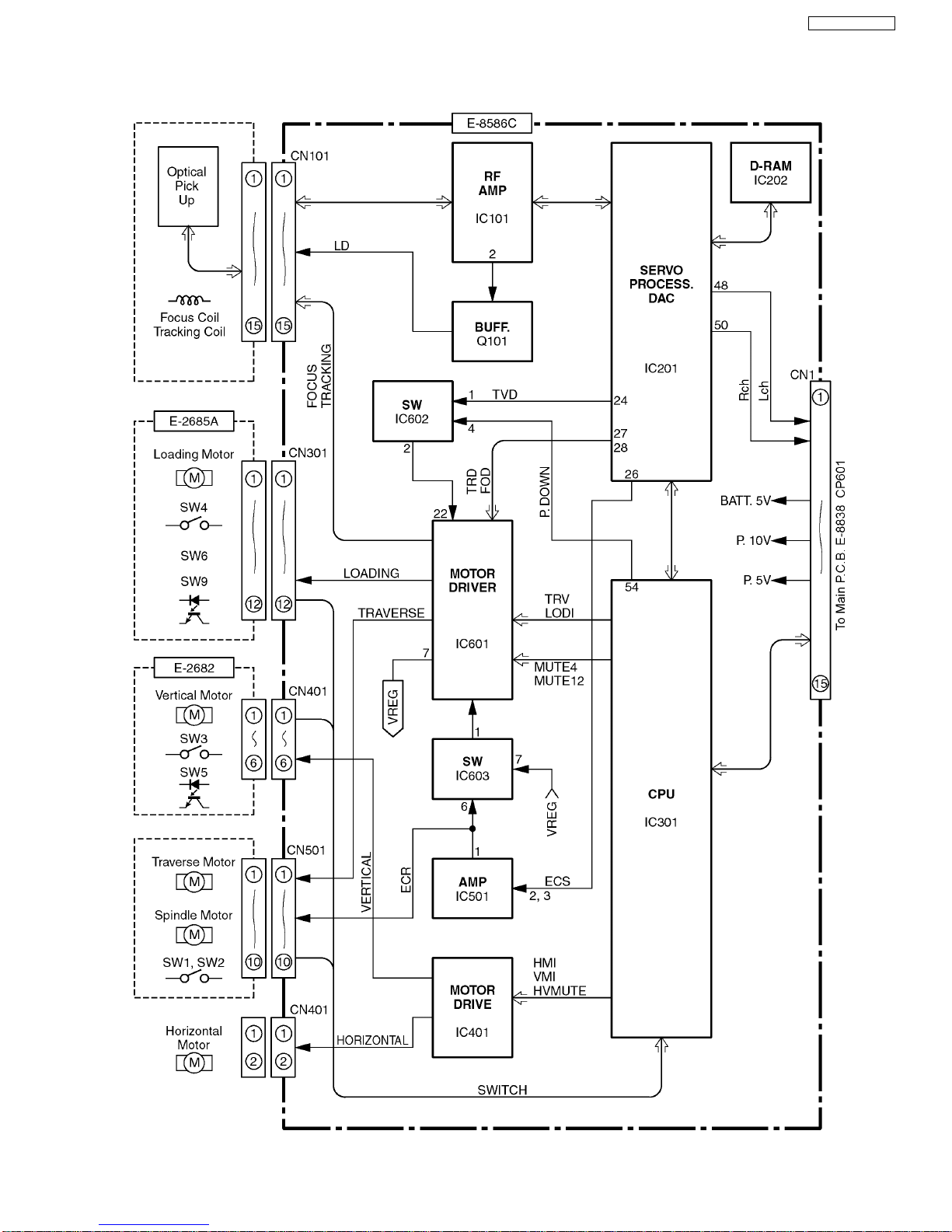
6.2. CD Servo Block
5
AUDI / CX-CA1090L

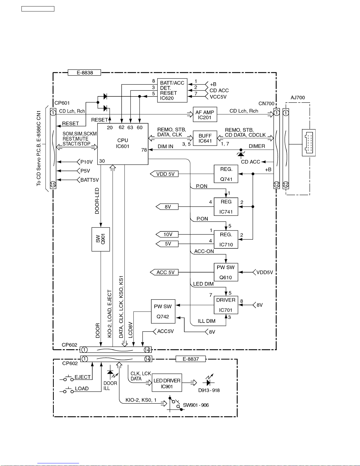
7.1. Main Block
IC600 : C2BBFE000088
Pin
No.
Port Description I/O (V)
1 CLK Shift clock LED data O 0
2 LCK Data loading clock O 0
3 - No connection - 4 AVSS Ground - 0
5 LCD DIM LCD dimmer control O 3.3
6 ILL DIM Not used - 7 AVref +5V power supply - 5.0
8 - No connection - -
9 ACC-ON ACC power control O 0
10 P.ON System power control O 5.0
11 NC No connection - 12 DATA Ext. CD.C data O 0
13 CLK Ext. CD.C clock O 0
14 STB Ext. CD.C strobe O 0
15 - No connection - 16 SOM CD.C serial data I 4.2
17 SIM CD.C serial data O 0
18 SCKM Clock for serial data O 5.0
19 CD ON CD.C start/stop O 5.0
20 /RESET CD.C reset O 5.1
21-24 - No connection - -
25 KS1 Key strobe O 0
26 KS0 Key strobe O 0
27 KI2 Key data I 0
28 KI1 Key data I 0
29 KI0 Key data I 0
30 DOOR-LED Door LED on/off O 0
31,32- No connection - -
33 VSS Ground - 0
34,35- No connection - -
36 TOC.CNT Not used - 37 MODE A Mode setting I 0
38 MODE B Mode setting I 0
39-59 - No connection - -
60 RESET Reset input I 4.6
61 - (Connecting to ground) - 0
62 BATT DET Battery level detection I 4.4
63 ACC DET ACC level detection I 4.4
64 EJECT Eject SW I 5.0
65 REMO Ext. CD.C remote control data I 4.8
66 LOAD CD disc loading SW I 5.0
67 - No connection - 68 VDD +5V power supply - 5.1
69 X2 Crystal oscillator - 2.4
70 X1 Crystal oscillator - 1.2
71 IC (Connecting to ground) - 0
72 XT2 Not used - 73 - (Connecting to ground) - 0
74 AVDD +5V power supply - 5.1
75 AVref +5V power supply - 5.0
76,77- No connection - -
78 DIM IN Dimmer signal I 0
79 NC No connection - 80 DATA Panel LED data O 0
7.2. CD Servo Block
IC201 : MN662783RPW
Pin
No.
Port Description I/O (V)
1 VDD +5V power supply - 5.0
2 D0 D-RAM data I/O 2.3
3 D1 D-RAM data I/O 1.8
4 /WE D-RAM data write O 4.9
5 /RAS D-RAM row address strobe O 3.4
6 D2 D-RAM data I/O 0.8
7 D3 D-RAM data I/O 0
8 /CAS0 D-RAM columun address strobe O 3.9
9 /CAS1 D-RAM columun address strobe O 0
10 A8 D-RAM address O 0.6
11 A7 D-RAM address O 1.1
12 A6 D-RAM address O 0.7
13 A5 D-RAM address O 0
14 A4 D-RAM address O 1.1
15 A9 D-RAM address O 0.4
16-18 A0 D-RAM address O 1.0
19 A3 D-RAM address O 0
20 VSS2 Ground - 0
21 VDD2 +5V power supply - 5.0
22,23 - Not used - -
24 TVD Traverse motor control O 2.5
25 PC Not used - 26 ECS Spindle motor control O 2.4
27 TRD Tracking coil drive O 2.5
28 FOD Focus coil drive O 2.4
29 FBAL Focus balance O 1.9
30 TBAL Tracking balance O 3.0
31 VREF Refence voltage I 2.5
32 FE Focus error I 2.5
33 TE Tracking error I 2.5
34 RFENV RF envelope I 2.5
35 OFT Off track signal I 0
36 /RFDET RF detecting signal I 0
37 BDO Drop-out signal I 0
38 LDON Laser on signal O 4.5
39 ARF RF signal I 2.5
40 IREF Reference current input I 1.2
41 DRF Bias for DSL I 2.4
42 DSLF Loop filter for DSL I/O 2.5
43 DSLF2 Loop filter for DSL I/O 2.2
44 PLLF Loop filter for PLL I/O 1.4
45 VCOF Not used - 46 AVDD2 +5V power supply - 5.0
47 AVSS2 Ground - 0
48 OUTL L channel output O 2.3
49 AVSS1 Ground - 0
50 OUTR R channel output O 2.3
51 AVDD1 +5V power supply - 4.7
52-54 - (Connecting to ground) - 0
55 FLAG Flag output O 0
56 FCLK Frame clock O 0
57-60 - Not used - -
61 MCLK Clock for I/F command I 1.0
62 MDATA Date for I/F command I 3.1
63 MLD I/F command load I 5.0
64 BLKCK Subcode block clock O 0
65 SQCK Ext.clock for sub code-Q I 5.0
66 SUBQ Code for sub. code-Q O 3.8
67 DMUTE Mute input I 0
68 STAT Status signal O 5.0
7 TERMINALS DESCRIPTION
6
AUDI / CX-CA1090L
69 /RST Reset input I 5.0
70 CSEL (Connecting to ground) - 0
71 PMCK Clock output O 2.5
72 SMCK Clock output O 2.5
73 SUBC Serial data of sub code O 0
74 SBCK Shift clock for SUBC I 0.6
75 /CLDCK Not used - 76 /TEST (Connecting to VDD) - 5.0
77 X1 Crystal oscillator - 0.4
78 X2 Crystal oscillator - 3.2
79 VDD1 +5V power supply - 5.0
80 VSS1 Ground - 0
IC301 : MN1873260AB
Pin
No.
Port Description I/O (V)
1 VDD +5V power supply - 5.0
2 OSC2 Crystal oscillator - 2.2
3 OSC1 Crystal oscillator - 2.1
4 VSS Ground - 0
5 XI (Connecting to ground) - 0
6 XO Not used - 7 CM (Connecting to ground) - 0
8 VREFH Reference voltage I 5.0
9 SW13 Shuter SW I 4.9
10 SW12 Horizontal origin I 4.9
11 SW11 Clump S W I 0
12 SW10 Play SW I 0
13 SW4 Shuter SW I 4.9
14 SW3 Tray origin SW I 0
15 SW2 Inner SW I 4.8
16 SW1 Outer SW I 4.9
17 VREFL Reference voltage I 0
18 /RESET Reset input I 4.9
19 - (Ground pull-down) - 0
20 SCKM Clock for serial data I 5.0
21 SIM CD changer serial data I 1.3
22 SOM CD changer serial data O 4.3
23 SQCK Ext. clock for sub. code-Q O 5.0
24 SUBQ Code for sub. code-Q I 1.6
25 - Not used - 5.0
26 - (Ground pull-down) - 0
27 CD.ON CD changer start/stop I 5.0
28 - Not used - 5.0
29 BLKCK Sub. code block clock I 0
30 P.ON Not used - 5.0
31 MUTE Mute output O 5.0
32 - (Ground pull-down) - 0
33 SENS Servo status O 0
34 CLVS Servo status O 5.0
35 FLOCK Focus servo lock O 0.2
36 TLOCK Tracking servo lock O 0
37 VMI Horizontal motor control O 2.5
38 HMI Vertical motor control O 0
39 HVMUTE H/V motor mute O 0
40-42 - (Ground pull-down) - 0
43 SW9 Disc-in (B) SW I 0
44 SW8 Disc-in (L) SW I 0
45 SW7 Disc-in (F) SW I 0
46 SW6 Disc push SW I 0
47 SW5 Tray hight SW I 4.5
48 BDO Drop-out signal I 0
49 DQSY Not used - 50 /RST Reset output O 5.0
51 STAT Status signal I 2.1
52 DMUTE Mute output O 0
53 XE Not used - 54 P.DOWN Power down signal O 0
55 - No connection - 56 MLD I/F command load O 5.0
57 MDATA Data for I/F command O 3.1
58 MCLK Clock for I/F command O 4.1
59 SPMT Spindle mute O 5.0
60 MUTE12 Focus/Tracking mute O 0
61 MUTE4 Loading motor mute O 4.8
62 LDOI Loading motor control I/O 2.5
63 TRV Forced traverse control I/O 2.4
64 SYNC Not used - -
7
AUDI / CX-CA1090L
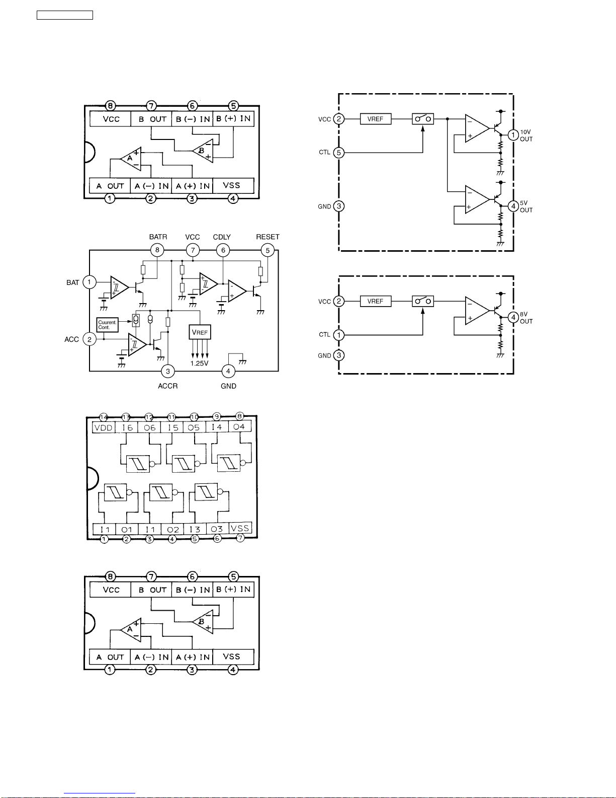
IC201 : YEAMPC4570T1
IC620 : AN8065SE1
IC641 : YEAMC14584BE
IC701 : C0ABBA000022
IC710 YEAMA61W12ST
IC741 : C0DAZHG00001
8 PACKAGE AND IC BLOCK DIAGRAM
8.1. Main Block
8
AUDI / CX-CA1090L
 Loading...