

ORDER NO. ACED070115C3
AUTOMOTIVE AFTERMARKET
CQ-C5305W
AAC WMA MP3 CD Player/Receiver
TABLE OF CONTENTS
PAGE P AGE
1 Service Navigation ----------------------------------------------- 2
2 Specifications ----------------------------------------------------- 3
3 Features -------------------------------------------------------------4
4 T ec hnic al Desc ri ptions----------------------------------------- 5
5 Block Diagram----------------------------------------------------10
6 Wiring Connection Diagram---------------------------------13
7 Schematic Diagram---------------------------------------------14
8 Schematic Diagram-2------------------------------------------17
9 Printed Circuit Board-------------------------------------------18
10 Exploded View and Replacement Parts List -----------23
11 Schematic Diagram for Printing with A4 Size----------32
© 2007 Matsushita Electric Industrial Co., Ltd. All
rights reserved. Unauthorized copying and distribution is a violation of law.
1 Service Navigation
1.1. About Lead Free Solder (PbF)
Distinction of PbF PCB :
• PCBs (manufactured) using lead free sol de r w ill ha ve a Pb F
stamp on the PCB.
Caution :
• Pb free solder has a higher melting point than standard solder; Typically the melting point is 50 - 70°F (30 - 40°C)
higher. Please use a soldering iron with temperature control
and adjust it to 700 ± 20°F (370 ± 10°C). In case of using
high temperature soldering iron, please be careful not to
heat too long.
• Pb free solder will tend to splash when heated too high
(about 1100°F/600°C)
• This lead free solder will be used for the products after serial
No. 1,000,001.
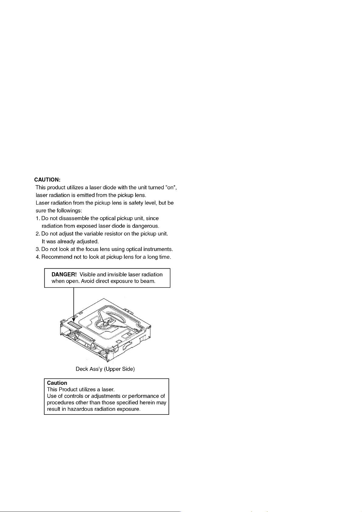
1.2. Laser Products
1.4. Maintenance
Your product is designed and manufactured to ensure a minimum of maintenance. Use a dry, a soft cloth for routine exterior
cleaning. Never use benzine, thinner or other solvents.
1.5. Notes
[RADIO BLOCK]
Do not align the AM/FM package block. When the package
block is necessary, it wi ll be sup pli ed alrea dy alig ne d at the fac tory.
[CD DECK BLOCK]
This model has no servo alignment points because microcomputer controls the servo circuit.
1.3. Replacing the Fuse
Use fuses of the same s pe cif ied rati ng 15 a mps. Using different
substitutes or fuses with higher ratings, or connecting the unit
directly without a fu se, could cause fire or dam ag e to th e s tere o
unit.
2
2 Specifications
2.1. Specifications*
General
Power Supply DC 12V (11V - 16V)
Current Consumption Less than 2.1A (CD mode, 0.5W 4-
Maximum Power Output 50W × 4 (at 1kHz), volume control maxi-
Power Output 18 W x 4 CH (1 kHz, 1 %, 4Ω )
Tone/SQ Adjustable
Range
Speaker Impedance 4 - 8 Ω
Pre-amp Output Voltage 2.5 V (CD mode: 1 kHz, 0 dB)
Subwoofer Output Voltage
Pre-amp Output Impedance
Subwoofer Output
Impedance
Front AUX Input
Input Impedance
Allowable External
Input
Connector
Test Voltage 14.4V
Negative Ground
Speaker)
mum
SQ Low/Bass:±12dB (at 60 Hz, 80 Hz , 100
Hz,200Hz)
SQ Mid: ±12 dB (at 500 Hz, 1 kHz , 2 kHz,
3kHz)
SQ High/Treble: ±12 dB (at 8kHz, 10kHz,
12 kHz, 15 kHz)
2.5 V (CD mode: 1 kHz, 0 dB)
200 Ω
200 Ω
10 kΩ
2.0 V
3.5 mm Stereo mini-pin
* Specifications and the design are subject to possible modification
without notice due to improvements.
** Dimensions and Weight shown are approximate.
** Above specifications comply with EIA standards.
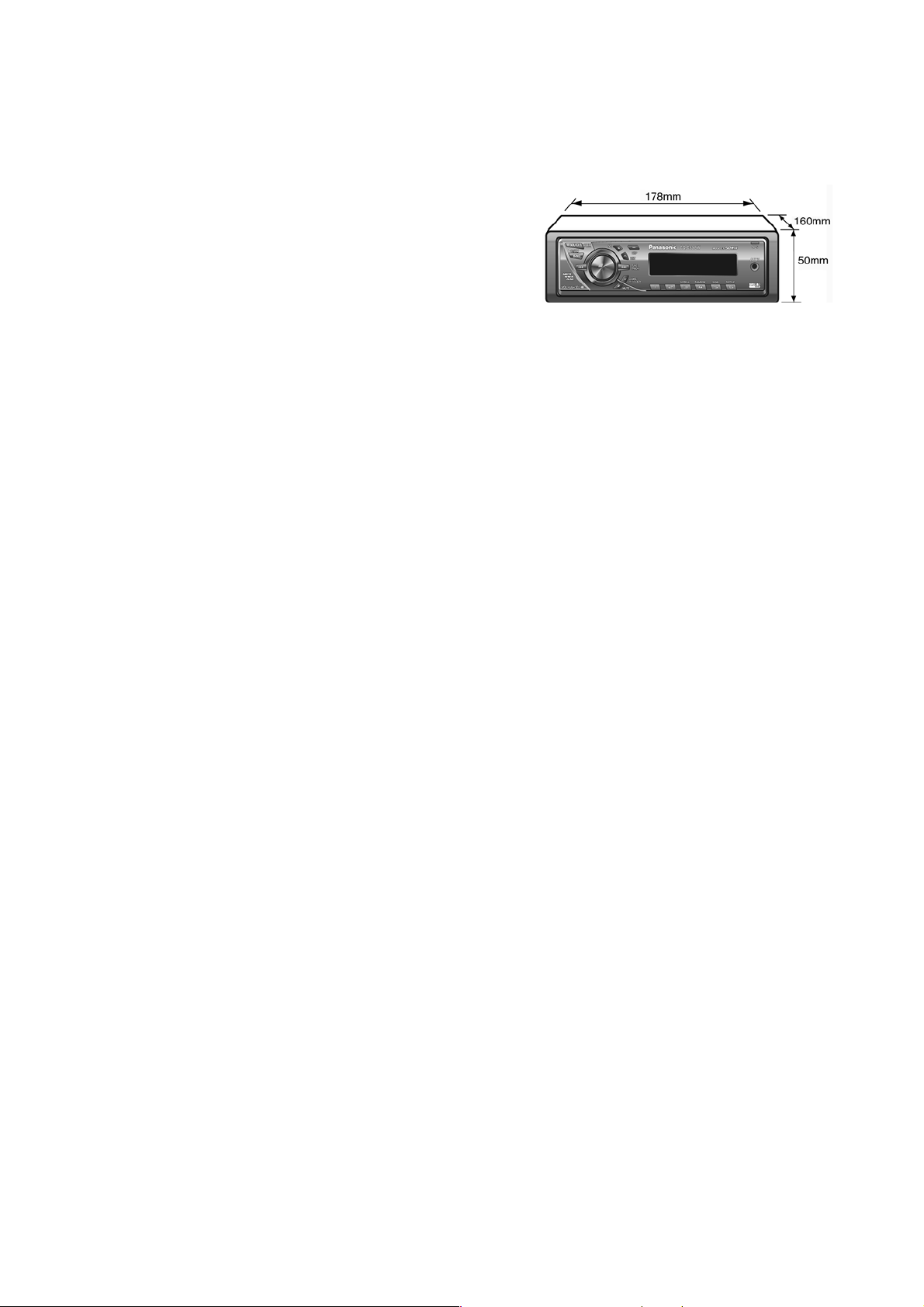
2.2. Dimensions
Dimensions (W×H×D)** 178×50×160mm
Weight** 1.3 kg
CD Player
Sampling Frequency 8 times oversampling
DA Converter 1 bit DAC System
Pick-Up Type Astigma 3-beam
Light Source Semiconductor Laser
Wave Length 790 nm
Frequency Response 20 Hz - 20 kHz (±1 dB)
Signal to Noise Ratio 96 dB
Total Harmonic Distortion
Wow and Flutter Below Measurable Limits
Channel Separation 75 dB
Stereo Radio
FM
Frequency Range 87.50 MHz - 108.00 MHz
Usable Sensitivity 6 dB/µV (S/N 30 dB)
Frequency Response 30 Hz - 15 kHz (±3 dB)
Alternate Channel Selectivity
Stereo Separation 35 dB (at 1 kHz)
Image Rejection Ratio 70 dB
IF Rejection Ratio 100 dB
Signal to Noise Ratio 62 dB
AM
Frequency Range 531 kHz - 1602 kHz
Usable Sensitivity 28 dB/µV (S/N 20 dB)
0.01 % (1 kHz)
75 dB
3

3 Features
• Hands Free Phone System. (The optional Bluetooth handsfree kit: CY-BT100N)
• Expansion Module (The optional Hub unit: CY-EM100N).
• The optional adapter allows you to connect the optional
Panasonic CD changer unit (CX-DP880 N ).
• The optional adapter allows you to connect the optional
iPod® series.
• SQ (Sound Quality).
• SQ3 (3-Band Sound Quality).
•SRS WOW
• The AUX Input terminal is equipped on the front panel.
• MP3/WMA/AAC Playback from CD-R/RW.
• Anti-Theft System.
4
4 Technical Descriptions
4.1. Terminals Description
4.1.1. Main Block
IC601 : YESAM397
Pin NoPort Description I/O Vol [V]
FM AM CD
1 DBGP0 Not connected - - - 2 DBGP1 Not connected - - - 3 DBGP2 Not connected - - - 4 RDS CLK Not connected - - - 5 RM DATA Remote control data I 4.7 4.7 4.7
6 CDC STB/
SYSID4
7 EVENT Hub event detection I 0 0 0
8 RESET System reset I 4.7 4.7 4.7
9 XT1 Crystal oscillator 1
10 XT2 Crystal oscillator 2
11 VSS Ground - 0 0 0
12 CF1 Ceramic oscillator 1
13 CF2 Ceramic oscillator 2
14 VDD +5V power supply - 4.8 4.8 4.8
15 INT A Pulled up for CQ-C5405U;
16 VSM Signal meter intensity
17 INT B Pulled down to GND - 0 0 0
18 LEVE L Not connected - - - 19 N.C. Not connected - - - 20 ACC ACC level detection I 4.9 4.9 4.9
21 SYSID1 Hub connection device
22 SYSID2 Hub connection device
23 N.C. Not connected - - - 24 CDC DATA Serial data from CD
25 CDC CLK/
SYSID3
26 CD DI (CD
SI)
27 CD DO (CD
SO)
28 CD CLK Serial clock for CD O 4.4 4.4 4.4
29 CD CE (FS) CD chip enable O 4.6 4.6 3.2
30 CD MUTE CD mute I 3.2 3.2 0
31 CD RST CD r eset O 4.8 4.8 4.8
32 POWER
CNT
33 N.C. Not connected - - - 34 N.C. Not connected - - - 35 CD SW1 CD detection switch 1 I 0 0 0
36 CD SW2 CD detection switch 2 I 0 0 0
37 N.C. Not connected - - - 38 N.C. Not connected - - - 39 VSS Ground - 0 0 0
40 VDD +5V power supply - 4.8 4.8 4.8
41 N.C. Not connected - - - 42 N.C. Not connected - - - 43 N.C. Not connected - - - -
CD changer Strobe; or
Hub connection device
identification 4
(32.768kHz)
(32.768kHz)
(13.5MHz)
(13.5MHz)
Pulled down for CQC5305U
(Tuner)
identification 1
identification 2
changer
Serial clock for CD
changer; or Hub connection device identification 3
Serial data from CD I 0 0 0
Serial data to CD O 0 0 0.6
System power supply control
I000
I111
O 1.4 1.4 1.4
I 1.4 1.4 1.4
O 1.3 1.3 1.3
I 4.8 4.8 4.8
I 0.2 0 0.2
I 4.8 4.8 4.8
I 4.8 4.8 4.8
I000
I000
O 4.8 4.8 4.8
Pin NoPort Description I/O Vol [V]
FM AM CD
44 N.C. Not connected - - - 45 HUB ACC
CNT
46 HUB CNT Hub connection check
47 INV CNT Not connected - - - 48 N.C. Not connected - - - 49 LCD DI Serial data to LCD O 4.7 4.7 4.7
50 LCD DO Serial data from LCD I 4.6 4.6 4.6
51 LCD CLK Serial clock for LCD O 4.8 4.8 4.8
52 LCD CE Chip enable for LCD CPU O 0 0 0
53 E-VOL I2C
DATA
54 E-VOL I2C
CLK
55 VDD +5V power supply - 4.8 4.8 4.8
56 VSS Ground - 0 0 0
57 E-VOL LV
CLK
58 E-VOL LV
DATA
59 STBY Standby mode for Power
60 SRS MODE 1Not connected - - - -
61 SRS MODE 2Not connected - - - -
62 SRS MODE 3Not connected - - - -
63 SRS
FOCUS
ELVL
64 EJ ILL Ejection key illumination
65 PANEL IN Front panel detection I 0 0 0
66 LCD 5V CNT +5V power supply control
67 N.C. Not connected - - - 68 EJECT Ejection switch I 4.8 4.8 4.8
69 BATT Battery level detection I 4.8 4.8 4.8
70 EXT MUTE Telephone mute I 4.8 4.8 4.8
71 OP/CL Open/Close detection for
72 MODE B
(ROTARY 2)
73 MODE A
(ROTARY 1)
74 CDC REM
OUT
75 HUB-TX Transmis sion data to Hub O 0 0 0
76 HUB-RX Reception data from Hub I 0 0 0
77 N.C. Not connected - - - 78 N.C. Not connected - - - 79 FM MODE Power supply control for
80 AM MODE Power supply control for
81 MONO Not connected - - - 82 ST FM stereo indication I 4.8 4.8 4.8
83 EE-PROM
DI/DO
84 EE-PROM CSNot connected - - - -
85 EE-PROM SKNot connected - - - -
86 ANT CNT Motor antenna driver con-
87 VREG Connected to capacitor - 3 3 3
Power supply control for
Hub (CD changer)
request
Serial data for Audio signal
processor (volume)
Serial data for Audio signal
processor
Serial clock to Audio signal
processor (Audio level)
Serial data from Audio signal processor (Audio level)
amplifier
Not connected - - - -
control
for LCD circuit
Front panel
Rotary encoder detection
B for volume
Rotary encoder detection
A for volume
Remote control for CD
changer
FM mode
AM mode
Not connected - - - -
trol
O0 0 0
O4.84.84.8
O4.84.84.8
O4.84.84.8
O0 0 0
I000
O4.84.84.8
O4.84.84.8
O0 0 0
I4.64.64.6
I4.84.84.8
I4.84.84.8
O0 0 0
O4.8 0 4.8
O04.80
-4.84.84.8
5
Pin NoPort Description I/O Vol [V]
FM AM CD
88 VSS Ground - 0 0 0
89 VDD +5V power supply - 4.8 4.8 4.8
90 OSC FM/AM FM/AM local oscillation fre-
quency
91 N.C. Ground - 0 0 0
92 FM/AM IFC FM/AM center frequency
input
93 N.C. Ground - 0 0 0
94 EO FM/AM phase detection
error output
95 SUBP D Not connected - - - 96 RDS DATA Not connected - - - 97 SSC SD sensitivity control O 0 0 0
98 AMP CNT Power supply control for
External amplifier
99 AF MUTE Audio signal mute O 4.8 4.8 4.8
100 AMP MUTE Mute for Power amplifier O 4.8 4.8 4.8
I1.41.40
I000
O2.22.1 0
O 4.7 4.7 4.7
4.1.2. Display Block
IC906 : YESAM246
Pin No. Port Description I/O (V)
1 SEG1/ P1 LED driver O 4.6
2 NC No Connected - 3 SEG3/ P3 LED (Red) driver O 4.6
4 SEG4/ P4 LED (Green) driver O 4.6
5 SEG5/ P5 LED (Blue) driver O 4.6
6-8 NC No Connection - -
9-70 SEG9-SEG70 LCD segment data O 2. 3
71-73 SEG71-73 Not connected - -
74 COM4 LCD comm on O 2.3
75 COM3 LCD comm on O 2.3
76 COM2 LCD comm on O 2.3
77 COM1 LCD comm on O 2.3
78-79 NC Not Connected - 80-83 KS3-6 Key scan O 4.6
84-88 KI1-5 Key data I 0
89 VDD +5V power supply - 4.6
90 VLCD LCD driver power supply - 4.6
91 VLCD1 VLCD1 filter terminal I 3.1
92 VLCD2 VLCD2 filter terminal I 1.5
93 VSS Ground - 0
94 TEST (Connecting to ground) I 0
95 OSC Oscillator terminal I/O 3.4
96 /RES Reset I 4.6
97 DO Key data output O 4.6
98 CE LCD driver chip enable I 0
99 CL LCD clock I 4.8
100 DI LCD data I 4.7
4.1.3. CD Servo Block
IC101 : YESAM383
Pin
No
1 P96 (A/D) Disc detection of CD deck
2 P95 (A/D) Reset switch detection of CD
3 P94 (A/D) Laser diode monitor I 2.1
4 P93 (A/D) GND - 0
5 P92 (A/D) GND - 0
6 P91 (A/D) GND - 0
7 P90 (A/D) GND - 0
8 P87/SRVMON1 Servo monitor 1 for O CD mod-
9 P86/SRVMON0 Servo monitor 0 for O CD mod-
10 P85 (A/D) CD mute control O 0
11 PB4 (A/D) Not connected - 12 P84 (A/D) Power-down detection I 1.2
13 DVSS3 GND - 0
14 SRAMVDD Power supply for SRAM I 1.5
15 REGOUT Regulated power supply O 1.5
16 REGVDD 3.3V power supply - 3.2
17 REGON2 Power control for internal regu-
18 P83 Not connected - 19 P82 Power control for OCD module O 3.2
20 P81/BA1 Not connected - 21 P80/BA0 G ND - 0
22 D2/P34 Not connected - 23 D1/P35 Not connected - 24 D0/P36 Not connected - 25 D3/P37 GND - 0
26 D4/P44 CD-mounting mode drive for
27 D5/P45 CD-ejection mode drive for Sled
28 D6/P46 Sled motor mode selection
29 D7/P47 CD servo mute (/RST) O 3. 2
30 D15/P60 GND - 0
31 D14/P61 GND - 0
32 D13/P62 GND - 0
33 D12/P63 GND - 0
34 D11/P64 GND - 0
35 D10/P65 GND - 0
36 D9/P66 GND - 0
37 D8/P67 GND - 0
38 SDRCK Not connected - 39 A11 Not connected - 40 A9 Not connected - 41 A8 Not connected - 42 A7 Not connected - 43 A6 Not connected - 44 A5 Not connected - 45 A4 Not connected - 46 NEW Not connected - 47 NCAS Not connected - 48 NRAS Not connected - 49 A3 Not connected - 50 A2 Not connected - 51 A1 Not connected - 52 A0 Not connected - 53 A10 Not connected - 54 VSSIC/N.C. GND - 0
55 IOVDD1 3.3V power supply - 3.2
56 DVDD1 1.5V power supply O 1.5
Port Description I/O (V)
I0
(SW1)
I3.2
deck
O0
ule
O0
ule
I3.2
lator
O0
Sled motor (LD-MT)
O0
motor (LD-EJ)
O3.2
(CNT)
6
Pin
No
57 FVDD/N.C. Connected with capacitor for
58 DVSS 1 GND - 0
59 FREGON Power control of internal regula-
60 SPOUT Spindle motor drive (ECS: Error
61 SPPOL Not connected - 62 TRVP Traverse mode dive for Sled
63 TRVM/P40 GND - 0
64 VPP/N.C. Not connected - 65 TRVP2 GND - 0
66 TRVM2/P41 GND - 0
67 TRP Tracking coil drive O 1.6
68 TRM/P42 GND - 0
69 FOP Focus coil drive O 2.1
70 FOM/P4 3 GND - 0
71 AVSS2 GND - 0
72 OSCIN Reference voltage I 1.6
73 CTRCRS Capacitor for T rack cross signal - 1.5
74 VREF Reference voltage O 1.6
75 E RF E from Pick-up unit I 2.0
76 F RF F from Pick-up unit I 2.0
77 D RF B from Pick-up unit I 1.8
78 B RF B from Pick-up unit I 1.8
79 C RF A from Pick-up unit I 1.8
80 A RF A from Pick-up unit I 1.8
81 PD Photo-diode sensor for Laser
82 LD Laser diode drive O 2.5
83 CENV Capacitor for Envelope signal - 1.8
84 RFENV RF envelope signal (connected
85 RFOUT CD RF signal O 1.2
86 RFIN CD RF signal I 1.7
87 AVDD2 3.3V power supply - 3.2
88 ARFDC DC component of RF - 1.1
89 ARFOUT RF signal O 1.2
90 ARFFB Feedback to RF amplifier - 1.2
91 ARFIN RF signal I 1.6
92 DSLF DSL loop filter I/O 1.6
93 IREF Reference current I 0.8
94 PLLF PLL filter I 1.4
95 PLLFO PLL filter O 1.4
96 VCOF VCO filter I/O 0
97 OUTL Analog audio L-ch signal O 1.6
98 AVSS1 GND - 0
99 AVREF Connected with capacitor - 1.6
100 AVDD1 3.3V power supply - 3.2
101 OUTR Analog audio R-ch signal O 1.6
102 TEST GN D - 0
103 CSEL GND - 0
104 PWMSEL PWM mode selection (pulled-
105 SRVMONON GND - 0
106 SEQMODE GND - 0
107 NRST CD reset from Main PCB I 3.2
108 IOVDD2 3.3V power supply - 3.2
109 X1 Crystal oscillator 1 (16.934MHz) I 1.5
110 X2 Crystal oscillator 2 (16.934MHz) O 1.6
111 DVSS2 GND - 0
112 MX1 GND - 0
113 MX2 Not connected - 114 IOVDD3 3.3V power supply - 3.2
115 MXSEL GND - 0
116 P00 Serial data from Main PCB (SO) O 0.7
Port Description I/O (V)
-1.8
regulator
I3.2
tor
O1.5
Correction of Servo)
O1.6
motor
I0
diode
-1.7
with capacitor)
I3.2
up)
Pin
No
117 P01 Serial data to Main PCB (SI) I 0
118 P02 Serial clock from Main PCB I 2.8
119 P03 Serial data for OCD (TDO) O 3.2
120 P04 Serial clock for OCD (TCLK) O 3.2
121 OCDSEL OCD (Optical scatterometry
122 P15 Not connected - 123 P16 Not connected - 124 P17 Not connected - 125 P20 3.3V power supply - 3.2
126 P21 CD ON control (CD FS) I 2.1
127 DVDD2 1.5V power supply I 1.5
128 P97 (A/D) Disc detection of CD deck
Port Description I/O (V)
O3.2
CD) module mode selection
I0
(SW2)
7
4.2. IC Block Diagram
4.2.1. Main Block
IC271 : YESAM274
IC650 : YESAM391
IC301 : YESAM357
IC602 : YESAM390
IC740 : YESAM269
IC750 : YESAM267
8
IC755 : YESAM347
IC791 : YESAM344
4.2.2. Display Block
IC905 : YESAM264
9
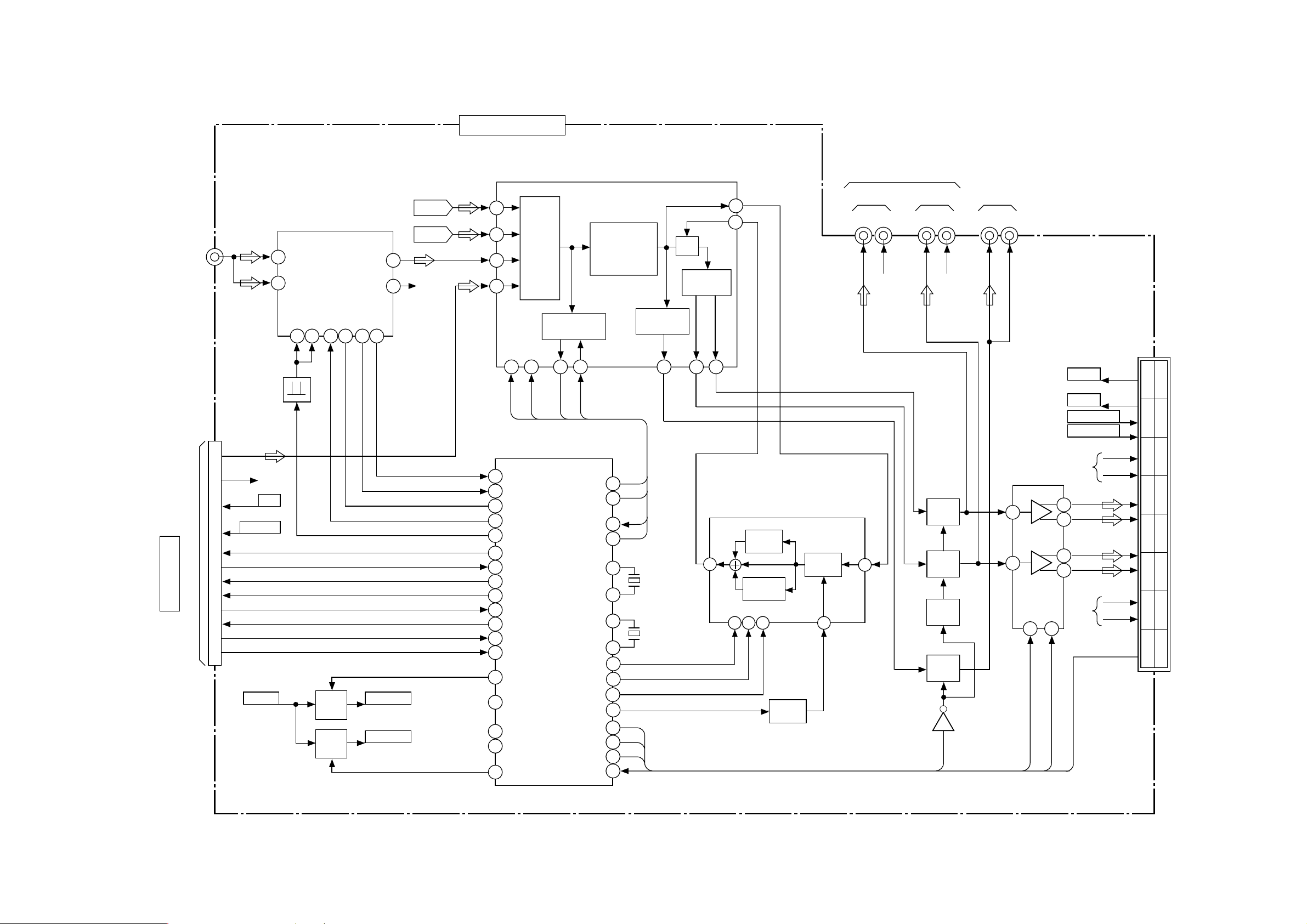
5 Block Diagram
5.1. Main-1 Block
7229-02-11(1/2)
AT051
ANT
CN801
CD-L
16
CD-R
17
9
10
(CD DECK)To
3032-14-49
13
7
CN101
8
5
6
3
4
2
1
CD SI
CD SO
CD SCK
CD FS
CD MUTE
CD RST
CD SW1
CD SW2
Q401
R-CH
9V
CD3.3V
TU+B
PA051
FM / AM TUNER
1
AM ANT
2 FM ANT
FM VT
AM VT
Q052,602
POW
SW
POW
SW
Q055,601
L-CH
R-CH
22212011146
VSM
SD / ST IND
FM / AM IFC
FM / AM OSC
FM VCC
AM VCC
16
17
AUX L
HUB L
R-CH
AUDIO SIGNAL PROCESSOR
7
5
INPUT
1
3
82
16
92
90
94
26
27
28
29
30
31
35
36
79
83
85
84
80
SEL
SPECTRUM
ANALIZER
SDA
SCLK
58
54
53
IC601(1/2)
SYSTEM CONTROL
ST
VSM
FM/AM IFC
FM/AM OSC
EO
CD SI
CD SO
CD SCK
CD FS
CD MUTE
CD RST
CD SW1
CD SW2
FM MODE
DI / DO
SK
CS
AM MODE
AMP MUTE
EXT MUTE
IC201
LOUDNESS
VOLUME
EQALIZER
57
53
SDA
54SCLK
58DATA
57CLK
XT1
XT2
10
CF1
12
CF2
13
60
61
62
63
99AF MUTE
59STBY
100
70
WOOFER
XL602
32.8KHz
9
XL601
13.5MHz
SRS1
SRS2
SRS3
SRS FOCUS
SUB
SW
SW
FADER
RL
16
14
FL
26242217182930
L
OUT
33
TRU
BASS
3D
STEREO
29 28 27 40
IC211
Q211
ELEV
CONT
FOCUS
CN250
PREOUT
FRONT REAR
LR LR LR
R-CH
L
IN
43
Q364
Q261
IC301
SRS WOW
AUDIO
Q345,346
Q251
R-CH
Q363
MUTE
MUTE
SW
MUTE
99
CN251
SUB.W
POWER AMP
12
14
IC271
STBY
59
21
23
MUTE
224
100
BATT
ACC
ANT CNT
AMP CNT
R-CH
FL+
5
FL-
3
RL+
RL-
R-CH
TEL MUTE
70
CN701
FR+
FR-
RR+
RR-
21
43
65
87
10 9
1211
1413
1615
10
CQ-C5305W MAIN(1/2)
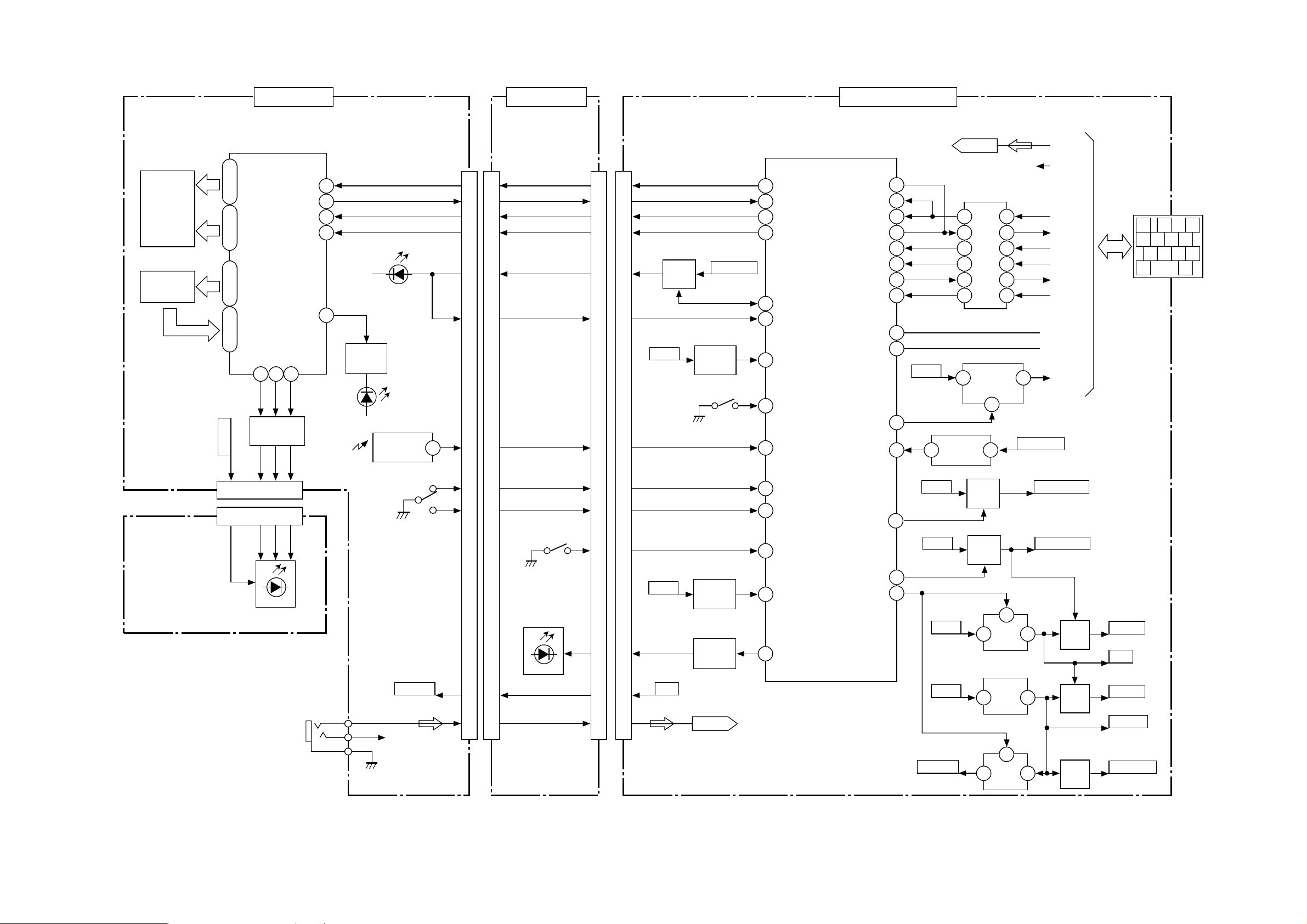
5.2. Main-2/Display/Connector Block
7229-02-11(2 / 2)7221-03-117229-05-11
LD901
KEY-IN
MATRIX
LCD DRIVE
SEG
1–62
COM
1–4
KS
3–6
KI
1–5
84–88 80–83 74–77 9–70
ILL9V
IC906
RED
GREEN
BLUE
345
LED
DRIVE
100
DI
97
DO
99
CL
98
CE
1
ILL
Q935–937
Q931
LED
DRIVE
RECEIVE
D901
IC905
IR
IC601(2/2)
SYSTEM CONTROL
CN971CN991 CN990CN901
CNT
75
76
24
74
25
6
46
7
21
22
45
8
BATT
12
11
11
10
12
3
5
5
3
LCD5V
6
2
OP/CL
12
10
RM DATA
1
2
6
99
1111
88
1212
Q972
1515
66
77
PWR
SW
BATT
VDD5V2
LCD5V CNT
Q701,702
BATT
CHECK
SW971
49
LCD DI
50
LCD DO
51
LCD CLK
52
LCD CE
66
71
OP/CL
69
BATT
65
PANEL IN
5
RM DATA
HUB TX
HUB RX
CDC DATA
CDC REMO
CDC CLK
CDC STB
HUB CNT
EVENT
HUB ACC
RESET
HUB L
IC650
6
3
8
12
11
2
1
IC602
RESET
INV
IC791
15V
LIMIT
2
R-CH
5
4
9
13
10
1
VDD5V2
3
L-CH
R-CH
DATA
REMO
SCLK
STRB
HCNT
EVENT
SYS ID1
SYS ID2
ACC
CN650
3
456
78910
11 12
2131
CN920
(CN910)
2413
2413
CN902
AUX
SW901
ILL9V
R-CH
14
13
4
9
8
9
4
13
ROT1
ROT2
SW990
1414
1313
11
22
1010
55
MODE A
MODE B
ACC
9V
R702,703
ACC
CHECK
Q971
LED
DRIVE
AUX L
73
ROTARY1
72
ROTARY2
68
EJECT
20
ACC
EJ ILL
64
ANT CNT
AMP CNT
POWER CNT
86
98
32
BATT
BATT
BATT
BATT
CD3.3V
Q703,751
PWR
SW
Q704,752
PWR
SW
IC750
IC755
4
12
REG
IC740
13
REG
1
45
REG
ANT CNT
AMP CNT
REG
Q750
PWR
SW
Q740
PWR
SW
Q770
TU+B
9V
SW5V
VDD5V
VDD5V2
11
CQ-C5305W MAIN(2/2)/DISPLAY/CONNECTOR
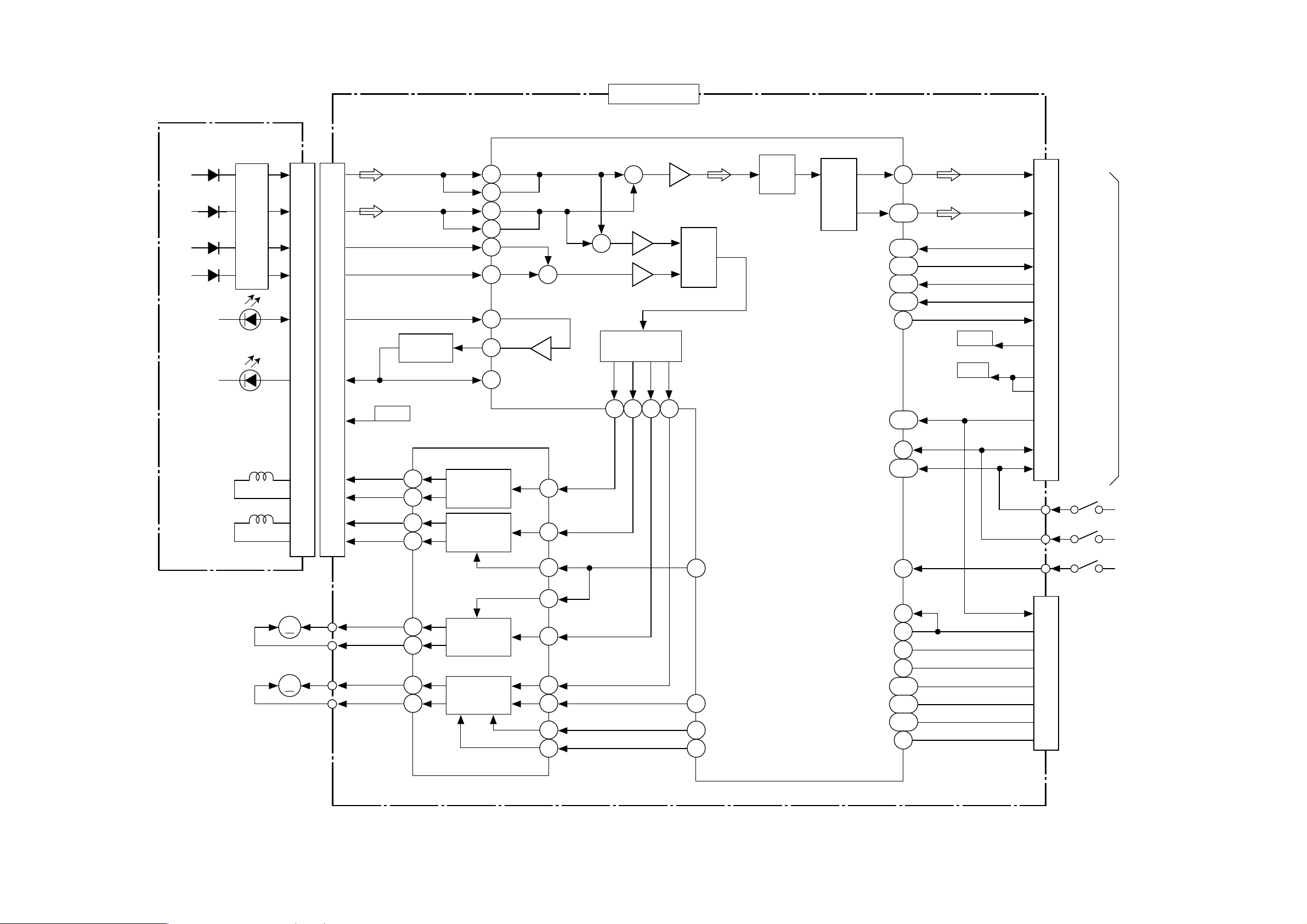
5.3. CD Servo Block
OPTICAL PICK-UP
A
B
E
F
PD
LD
FOCUS
COIL
TRACKING
COIL
I-V
AMP
CN102
7
9
3
2
11
4
1
15
16
13
14
LPD
LD
FF+
TT+
3.3V
Q101
LD
DRIVE
PICK-UP DRIVE
14
13
12
11
FOCUS
DRIVE
TRACKING
DRIVE
80
79
78
77
75
76
81
82
IC201
COIL
COIL
MUTE
LD MON
3
3032-14-49
IC101
RF AMP,SERVO,DSP
CN101
+
FE
EFM
DEM
DAC
-
TE
ADC
-
SERVO
CTL
69 67 60 62
ECS
TVD
2
RST
TRD
FOD
2
3
9
L
R
97
101
117
116
118
126
10
107
1
128
2
3.3V
8V
Lch
15
Rch
18
CD SI
8
CD SO
7
CD SCK
6
CD ON
5
CD MUTE
4
CD3.3V
14
DC8V
9
DC8V
10
CD RST
3
1
SW1
2
SW2
To
MAIN
CN801
SW2
SW1
RESET
SPINDLE
MOTOR
SLED
MOTOR
M
M
18
17
16
15
MUTE
SPINDLE
MOTOR
DRIVE
SLED
MOTOR
DRIVE
27
5
26
24
20
28
MUTE
12
27
26
28
LD EJ
LD MT
CNT
19
17
9
8
120
119
121
12
CQ-C5305W CD DECK
CN103
9
NRST
1
REGON2
4
SRVMON0
5
SRVMON1
6
TCLK
7
TDO
DMODE
11
NPWDOWN
13

6 Wiring Connection Diagram
4
/
4
/
Rear Speakers
Front Speakers
External Mute
Motor Antenna Relay Control
External Amplifier Control
Battery(15A)
Ground
Power (ACC or IGN)
L
R
<S.W-OUT>
Power
Connector
2
13 1
CN701
Main P.C.B
[7229-02-11]
17
1
2
18
CN801
Extension
Connector
Jig Part No.
[YESFZS2067]
System
up
10
12
CN650
Preamp Out
(Front) (Rear)
7
11
31
CN971
1
2
CN250
64
4
1
CN251
17
Loading/Feed
Reset
SW
Optical
5
AT051
Pic-Up
Ass'y
SW2
CN102
SW1
Spindle
Motor
1
17
18
2
1
17
CN101
CD Servo P.C.B
[3032-14-49]
(Bottom View)
Motor
Extension
Connector
Jig Part No.
[YESFZS2068]
(CN910)
1
CN990
1
CN991
14
CN920
3
1
Display P.C.B
2
4
[7229-05-11]
(Bottom View)
3
1
2
4
7
8
CN901
Connector P.C.B
17
7
8
1
14
(Bottom View)
CN902
3
2
1
AUX
[7221-03-11]
13

7 Schematic Diagram
N
7.1. Main Block
PA051
YESAP403
(AM)
FM
(0)
0
(0)
0
(-)
IC601
1
2
3
4
5
6
7
8
9
10
11
12
13
14
15
16
17
18
19
20
21
22
23
24
25
0
0
0
1.3
0
0
0
0
0
8.3
8.4
1.3
0
3.7
3.7
0
0
0
4.8
0
0
8.4
-
Q770
YESAN087
FM
-
-
0
4.7
0
0
4.7
1.0
1.4
0
1.4
1.3
4.8
4.8
0.2
0
-
-
4.9
4.8
4.8
0
0
(-)
(0)
(2.0)
(0)
(0)
(8.3)
(0)
(0)
(0)
(8.4)
(2.0)
(0)
(3.7)
(3.7)
(0)
(-)
(0)
(0)
(4.8)
(0)
(0)
(8.4)
(-)
D770
AM
D979
8V
Q055
YESAN117
8V
YESAN117
L
R
8V
8.5
9.0
9.1
YESAD123
FM
CD
0
-
-
26
0
-
-
27
4.4
-
-
28
4.6
0
0
29
3.2
4.7
4.7
30
4.8
0
0
31
4.8
0
0
32
-
4.7
4.7
33
-
1.0
1.0
34
0
1.4
1.4
35
0
0
0
36
-
1.4
1.4
37
-
1.3
1.3
38
0
4.8
4.8
39
4.8
4.8
4.8
40
-
0.2
0
41
-
0
0
42
-
-
-
43
-
-
-
44
0
4.9
4.9
45
4.8
4.8
4.8
46
-
4.8
4.8
47
-
-
-
48
4.7
0
0
49
4.6
0
0
50
The following symbols are
shown on the schematic
diagram.
9V
8V
5V
3.3V
YESAD155
8.3
8.4
8V
Q052
8V
AM
CD
0
0
0
0.6
4.4
4.4
4.6
3.2
3.2
0
4.8
4.8
4.8
4.8
-
-
-
-
0
0
0
0
-
-
-
-
0
0
4.8
4.8
-
-
-
-
-
-
-
-
0
0
4.8
4.8
-
-
-
-
4.7
4.7
4.6
4.6
+B
Acc
9V
8V
5V
3.3V
RADIO (L,R)
CD (L,R)
AUDIO(L,R)
0
8.4
8.4
51
52
53
54
55
56
57
58
59
60
61
62
63
64
65
66
67
68
69
70
71
72
73
74
75
Q601
YESAN122
0
Q602
YESAN122
0
0
D053 YESAD119
9V
FM
AM
4.8
4.8
0
0
4.8
4.8
4.8
4.8
4.8
4.8
0
0
0
0
0
0
4..8
4.8
0
0
0
0
0
0
0
0
4.8
4.8
0
0
0
0
-
-
4.8
4.8
4.8
4.8
4.8
4.8
4.6
4.6
4.8
4.8
4.8
4.8
0
0
0
0
4.8
0
8.4
0
R
CD
AM
CD
FM
4.8
0
0
76
0
-
-
77
4.8
-
-
78
4.8
0
4.8
4.8
79
4.8
4.8
0
80
0
-
-
81
0
4.8
4.8
4.8
82
0
-
-
83
-
4.8
-
84
-
0
-
85
4.8
0
4.8
86
3.0
0
0
4.8
0
0
-
4.8
4.8
4.8
4.6
4.8
4.8
0
0
3.0
3.0
87
0
0
88
4.8
4.8
4.8
89
1.4
1.4
90
0
0
91
0
0
92
0
0
93
2.1
2.2
94
-
-
95
-
-
96
0
0
97
4.7
4.7
4.7
98
4.8
4.8
4.8
99
4.8
4.8
4.8
100
S.W-OUT
7229-02-11
Q263,346
YESAN121
0
0
Q261
YESAN118
00
0
0
-0.3
-0.3
0
0
0
Q263
0
0
0
0
0
0
0
0
0
0
Q264,363,364
YESAN121
SW971
YEAS08042
D991
YESAD155
D601
5V
0
IC602
YESAM390
4.7
2V/DIV,20us/DIV
YESAD143
4.7
4.8
D976,978
YESAD133
0
4.8
Q972
YESAN120
18
18
1V/DIV,0.1us/DIV
5V
To CD Servo
L
D977
YESAD150
L
R
R
18
18
18
IC601
YESAM397
2V/DIV,1ms/DIV
2V/DIV,0.1s/DIV
2V/DIV,50ms/DIV
3032-14-49 CN101
R
5V
Q971
YESAN120
9V
LR
4.8
4.804.804.8
IC650 YESAM391
4.800.4
2V/DIV,50ms/DIV
5V
D650
YESAD144
5V
5V
3.3V
8V
R
8V
L
L
R
L
18
2V/DIV,50ms/DIV
2V/DIV,20ms/DIV
2V/DIV,50ms/DIV
4.8
4.8
0
0
4.8
4.200
D651
YESAD119
RL
RR
FL
FR
180
180
180
180
180
0
L
R
RLFLFRRR
9V
L
R
R
4.8
8.6
8.7
IC201 YESAM384
4.3
4.3
R
L
L
L
4.3
4.3
4.3
0.6
4.3
4.3
4.2
4.2
4.2
4.3-4.3
4.3
4.3-4.3
R
L
R
4.3
4.8
0
4.3
4.3
4.3
4.3
8V
3.3V
5V 5V
9V
5V
9V
R
L
R
L
8V
3.3V
5V
Q345
YESAN118
Q251
YESAN128
4.8
0
4.8
L
1.3
2.2
0
Q401
B1CBGF000005
(J)
0
-
0
-
-
-
0
0
0
0
0
0
0
-
9V
0
L
R
IC271 YESAM274
0
0
7.2
4.7
7.1
7.207.2
9.0
3.8
3.803.8
3.8
3.8
7.207.2
7.2
4.5
7.1
14.8
RL
RR
14.8
D278 YESAD146
D279
YESAD146
FL
FL
FR
FR
RR
RL
D270-D277
YESAD146
5V5V
D704
YESAD143
D705 YESAD146
D701 YESAD139
D703
YESAD119
D706 YESAD146
1/4W
YESAN115
0
0
YESAN123
YESAN126
Q704
14.4
14.4
4.9
YESAN123
4.8
4.8
Q701
D702 YESAD153
Q752 YESAN115
14.8 14.8
14.8
5.1
0
4.8
0
Q702
YESAN129
0
0
0
0.9
14.8
14.8
14.4
14.4
14.4
4.7
R
IC750 YESAM267
5V
D761 YESAD140
9V
8V
5V
D795
YESAD144
5V
3.3
IC755
YESAM347
0
1.2
D755
YESAD146
5V
4.1
4.8
9V
L
0
0
IC301 YESAM357
IC211
YESAM398
9V
YESAN122
8V
3.3V
5V
5V
9V
R
9V
5V
3.3V
5V
8V
Q211
YESAD144
D760 YESAD146
Q750
YESAN079
4.8 4.8
5.4
D741
1SS133T77
4.8 4.8
5.4
9V9V
D791 YESAD146
D762
Q740
YESAN079
5V
IC740 YESAM269
IC791 YESAM344
4.8
4.8
4.8
14.4
9.004.8
D750
YESAD141
14.404.8
4.8
14.8
D980
YESAD155
To Connector 7221-03-11 CN990
CQ-C5305W MAI
14

7.2. Display Block
D921-D934
YESAD166
9V
IC905
YESAM264
7229-05-11
SW902-SW916
K0H1BA000445
D966
YESAD173
0.2
0
D901
YESAD166
L
0.7
Q931
YESAN146
LIST
4.704.6
SW901
YESAS123
2V / DIV, 2ms / DIV
2.3
2.3
2.3
2.3
2.3
2.3
2.3
2.3
2.3
2.3
2.3
2.3
2.3
2.3
2.3
2.3
2.3
2.3
2.3
2.3
2.3
2.3
2.3
2.3
5V
D912
YESAD147
5V
D913
YESAD150
5V
5V
To CN
CN991
7221-03-11
R
5V
9V 9V
YESAD143
D970
D972
YESAD119
5V
4.6
4.6
4.6
4.6
0
0
0
0
0
4.6
4.6
3.1
1.5
0
0
3.4
4.6
4.6
0
4.8
4.7
2V / DIV, 2ms / DIV
2V / DIV, 10us / DIV
2V / DIV, 50ms / DIV
2V / DIV, 50ms / DIV
4.6
4.6
4.6
4.6
1V / DIV, 2ms / DIV
YESAM246
2.3
2.3
2.3
IC906
2.3
2.3
2.3
2.3
2V / DIV, 2ms / DIV
1V / DIV, 2ms / DIV
2.3
2.3
2.3
2.3
2.3
2.3
2.3
2.3
2.3
2.3
2.3
2.3
2.3
2.3
2.3
2.3
2.3
2.3
2.3
2.3
2.3
2.3
2.3
2.3
2.3
2.3
2.3
2.3
2.3
2.3
2.3
2.3
2.3
2.3
2.3
D911 YESAD150
9V
1/4W
Q936
0
0
0
0
0.7
Q935
YESAN146
0.7
0.7
The following symbols are
shown on the schematic
diagram.
9V
9V
5V
5V
AUDIO (L,R)
LD901 YESXDCM041
1/4W
YESAN146
1/4W
0
Q937
0
YESAN146
L
R
(
)
9V
D935
YESAD169
D936
YESAD169
CQ-C5305W DISPLAY
15

7.3. CD Servo Block
3032-14-49
8V8V8V
1.6
1.7
1.6
1.6
1.6
IC201
1.6
0
0
0
8.3
3.2
3.2
1.6
1.101.6
3.3V
8.3
3.204.6
4.6
4.3
4.8
YESAM339
0
0
8.3
3.7
4.1
3.9
3.9
3.3V
3.1
2.5
1.8
Q101
YESAN086
The following symbols are
shown on the schematic
diagram.
8V
8V
3.3V
3.3V
CD(L,R)
0
3.2
1.5
1.803.2
1.5
1.6
0
0
0
1.6
0
2.1
0
0
1.6
1.5
1.6
2.0
2.0
1.8
1.8
1.8
1.8
0
2.5
1.8
1.7
1.2
1.7
3.3V
3.3V
3.3V
3.2
1.1
1.2
1.2
1.6
1.6
0.8
1.4
1.4
0
L
1V / DIV, 5µs / DIV
1V / DIV, 10µs / DIV
1V / DIV, 0.1ms / DIV
0.5V / DIV, 50ns / DIV
0
1.6
3.2
1.601.6
R
0
0
3.2
2V / DIV, 50ns / DIV
0
1.5
3.2
3.2
IC101
YESAM383
2V / DIV, 0.1s / DIV
0
0
1.6
2V / DIV, 50ms / DIV
2V / DIV, 1ms / DIV
3.2
2.800.703.2
2V / DIV, 50ms / DIV
3.2
3.2
00000
0
0
0
3.2
3.2
0
0
0
0
0
0
0
3.2
0
3.2
3.2
1.5
1.5
0
1.2
0
0
0
0
0
0
0
0
2.1
3.2
0
0
1.5
2.1
3.2
3.3V
(CN103)
3.3V
8V 8V
D103 YESAD177
3.3V
3.3V
8V
L
To MAIN 7229-02-11 CN801
R
3.3V3.3V3.3V
3.3V
R
3.3V
R
16
L
3.3V3.3V
L
3.3V
CQ-C5305W CD SERVO

8 Schematic Diagram-2
N
8.1. Connector Block
D990
YESAD165
D995
YESAD155
CQ-C5305W C
AUX Lch
CN901
7229-05-11
To DISPLAY
AUX GND
1K
1/4W
R
L
AUX Rch
5V
9V
5V
7221-03-11
RL
K0H1BA000445
9V
To MAIN 7229-02-11 CN971
AUX Lch
AUX GND
RL
D991
YESAD165
1K
1/4W
AUX Rch
9V5VAUDIO (L,R)
9V
5V
The following symbols are
shown on the schematic
diagram.
17

9 Printed Circuit Board
9.1. Main/Connector Block (Top View)
18

9.2. Main/Connector Block (Bottom View)
19

9.3. Dis p lay Block
20

9.4. CD Servo Block (Top View)
21

9.5. CD Servo Block (Bottom View)
22

10 Exploded View and Replacement Parts List
A
B
C
D
E
10.1. Exploded View
1234
40
44
43
Display P.C.B
[7229-05-11]
A
41
42
55
49
50
105
105
48
< Installation Parts
Mounting Collar >
45
46
105
54
53
B
52
51
47
56
102
1
6
101
92
CD Deck
Ass'y
A
2
101
C
104
21
100
106
23
107
28
27
D
26
29
100
AT001
CN801
PA051
CN971
AT051
22
A
4
101
35
E
< Installation Parts
Trim Plate >
103
106
34
33
32
25
31
Connector P.C.B
[7221-03-11]
30
AT002
103
20
Main P.C.B
[7229-02-11]
7
CQ-C5305W
1234
23

10.2. Replacement Parts List
Notes :
1. Be sure to make you r orde rs of repl acem ent p arts acco rding to this list.
2. Important safety notice: Components, identified by
mark have special characteristics important for safety.
When replacing any of these components, use only manufacturer's specified parts.
3. Location keys in the remarks column indicates the general location of the parts shown in the exploded drawing,
as in a road map.
4. The marking (RTL) indicates that Retention Time is limited for this item. After the discontinuation of assembly in
production, the item will continue to be available for a
specific pe ri od of time . Th e re tent ion p er iod of avai lab ili ty
is dependent on the type of assembly, and in accordance
with the laws governing part and product retention. After
the end of this period, the assembly will no longer be
available.
• Order intak e period is basi cally s ix month s after t he fir st
shipment.
Ref. No. Part No. Part Name & Description Remarks
[7229-02-11] Main Block
IC's and TRANSISTORs
IC201 YESAM384 IC
IC211 YESAM398 IC
IC271 YESAM274 IC
IC301 YESAM357 IC
IC601 YESAM397 IC
IC602 YESAM390 IC
IC650 YESAM391 IC
IC740 YESAM269 IC
IC750 YESAM267 IC
IC755 YESAM347 IC
IC791 YESAM344 IC
PA051 YESAP403 Tuner Pack
Q052 YESAN117 Transistor
Q055 YESAN117 Transistor
Q211 YESAN122 Transistor
Q251 YESAN128 Transistor
Q261 YESAN118 Transistor
Q263 YESAN121 Transistor
Q264 YESAN121 Transistor
Q345 YESAN118 Transistor
Q346 YESAN121 Transistor
Q363 YESAN121 Transistor
Q364 YESAN121 Transistor
Q401 B1CBGF000005 FET
Q601 YESAN122 Transistor
Q602 YESAN122 Transistor
Q701 YESAN126 Transistor
Q702 YESAN129 Transistor
Q703 YESAN123 Transistor
Q704 YESAN123 Transistor
Q740 YESAN079 Transistor
Q750 YESAN079 Transistor
Q751 YESAN115 FET
Q752 YESAN115 FET
Q770 YESAN087 Transistor
Q971 YESAN120 Transistor
Q972 YESAN120 Transistor
DIODEs
D053 YESAD119 Zener Diode
D270 YESAD146 Diode
D271 YESAD146 Diode
D272 YESAD146 Diode
Ref. No. Part No. Part Name & Description Remarks
D273 YESAD146 Diode
D274 YESAD146 Diode
D275 YESAD146 Diode
D276 YESAD146 Diode
D277 YESAD146 Diode
D278 YESAD146 Diode
D279 YESAD146 Diode
D601 YESAD143 Diode
D650 YESAD144 Diode
D651 YESAD119 Zener Diode
D701 YESAD139 Diode
D702 YESAD153 Zener Diode
D703 YESAD119 Zener Diode
D704 YESAD143 Diode
D705 YESAD146 Diode
D706 YESAD146 Diode
D741 1SS133T77 Diode
D750 YESAD141 Diode
D755 YESAD146 Diode
D760 YESAD146 Diode
D761 YESAD140 Diode
D762 YESAD144 Diode
D770 YESAD123 Zener Diode
D791 YESAD146 Diode
D795 YESAD144 Diode
D976 YESAD133 Zener Diode
D977 YESAD150 Zener Diode
D978 YESAD133 Zener Diode
D979 YESAD155 Diode
D980 YESAD155 Diode
D991 YESAD155 Diode
CAPACITORs
C61 YESCC447 Ceramic, 0.022µF 25WV
C62 YESCC447 Ceramic, 0.022µF 25WV
C051 YESCC478 Ceramic, 47pF 50WV
C052 YESCC483 Ceramic, 0.1µF 50WV
C053 YESCC482 Ceramic, 0.01µF 50WV
C055 YESCC482 Ceramic, 0.01µF 50WV
C058 YESCC482 Ceramic, 0.01µF 50WV
C065 YESCC481 Ceramic, 0.001µF 50WV
C067 YESCC482 Ceramic, 0.01µF 50WV
C071 YESCC559 Ceramic, 0.012µF 50WV
C201 YESCC556 Ceramic, 0.33µF 16WV
C202 YESCC589 Electrolytic, 3.3µF 50WV
C203 YESCC590 Electrolytic, 1µF 50W V
C204 YESCC522 Ceramic, 1µF 16WV
C210 YESCC522 Ceramic, 1µF 16WV
C211 YESCC546 Electrolytic, 10µF 16WV
C220 YESCC523 Ceramic, 0.1µF 16WV
C221 YESCC365 Electrolytic, 120µF 10WV
C245 YESCC372 Electrolytic, 4.7µF 25WV
C255 YESCC549 Electrolytic, 2.2µF 50WV
C261 YESCC372 Electrolytic, 4.7µF 25WV
C262 YESCC372 Electrolytic, 4.7µF 25WV
C263 ECQV1H224JL2 Plastic Film, 0.22µF 50WV
C267 ECQV1H224JL2 Plastic Film, 0.22µF 50WV
C271 YESCC486 Ceramic, 0.0047µF 50WV
C272 YESCC486 Ceramic, 0.0047µF 50WV
C273 YESCC434 Ceramic, 330pF 50WV
C274 YESCC434 Ceramic, 330pF 50WV
C276 YESCC597 Electrolytic, 10µF 16WV
C277 YESCC452 Ceramic, 1µF 16WV
C278 YESCC596 Ceramic, 0.1µF 16WV
C279 YESCC368 Electrolytic, 2200µF 16WV
C291 YESCC481 Ceramic, 0.001µF 50WV
C292 YESCC481 Ceramic, 0.001µF 50WV
C301 YESCC556 Ceramic, 0.33µF 16WV
C302 YESCC589 Electrolytic, 3.3µF 50WV
C303 YESCC590 Electrolytic, 1µF 50W V
C304 YESCC522 Ceramic, 1µF 16WV
24

Ref. No. Part No. Part Name & Description Remarks
C311 YESCC523 Ceramic, 0.1µF 16WV
C312 YESCC442 Ceramic, 0.01µF 50WV
C313 YESCC523 Ceramic, 0.1µF 16WV
C314 YESCC523 Ceramic, 0.1µF 16WV
C315 YESCC523 Ceramic, 0.1µF 16WV
C316 YESCC523 Ceramic, 0.1µF 16WV
C317 YESCC523 Ceramic, 0.1µF 16WV
C318 YESCC523 Ceramic, 0.1µF 16WV
C319 YESCC522 Ceramic, 1µF 16WV
C320 YESCC531 Ceramic, 10µF
C321 YESCC448 Ceramic, 0.033µF 25WV
C326 YESCC547 Electrolytic, 100µF 16WV
C327 YESCC531 Ceramic, 10µF
C328 YESCC531 Ceramic, 10µF
C322 YESCC442 Ceramic, 0.01µF 50WV
C323 YESCC556 Ceramic, 0.33µF 16WV
C324 YESCC557 Ceramic, 0.47µF 16WV
C325 YESCC432 Ceramic, 220pF 50WV
C332 YESCC574 Electrolytic, 10µF 16WV
C333 YESCC574 Electrolytic, 10µF 16WV
C334 YESCC523 Ceramic, 0.1µF 16WV
C335 YESCC523 Ceramic, 0.1µF 16WV
C336 YESCC574 Electrolytic, 10µF 16WV
C337 YESCC574 Electrolytic, 10µF 16WV
C361 YESCC372 Electrolytic, 4.7µF 25WV
C362 YESCC372 Electrolytic, 4.7µF 25WV
C363 ECQV1H224JL2 Plastic Film, 0.22µF 50WV
C367 ECQV1H224JL2 Plastic Film, 0.22µF 50WV
C371 YESCC486 Ceramic, 0.0047µF 50WV
C372 YESCC486 Ceramic, 0.0047µF 50WV
C373 YESCC434 Ceramic, 330pF 50WV
C374 YESCC434 Ceramic, 330pF 50WV
C375 YESCC598 Electrolytic, 0.47µF 50WV
C378 YESCC596 Ceramic, 0.1µF 16WV
C380 YESCC596 Ceramic, 0.1µF 16WV
C390 YESCC563 Ceramic, 2.2µF
C391 YESCC563 Ceramic, 2.2µF
C401 YESCC599 Electrolytic, 220µF 10WV
C402 ECQV1H683JL2 Plastic, 0.068µF 50WV
C403 YESCC562 Ceramic, 0.0068µF 50WV
C404 YESCC482 Ceramic, 0.01µF 50WV
C430 YESCC599 Electrolytic, 220µF 10WV
C601 YESCC600 Ceramic, 27pF 50WV
C602 YESCC477 Ceramic, 22pF 50WV
C603 YESCC531 Ceramic, 10µF
C604 YESCC523 Ceramic, 0.1µF 16WV
C605 YESCC523 Ceramic, 0.1µF 16WV
C606 YESCC603 Electrolytic, 1000µF 6.3WV
C607 YESCC523 Ceramic, 0.1µF 16WV
C608 YESCC430 Ceramic, 100pF 50WV
C609 YESCC452 Ceramic, 1µF 16WV
C610 YESCC442 Ceramic, 0.01µF 50WV
C611 YESCC442 Ceramic, 0.01µF 50WV
C612 YESCC442 Ceramic, 0.01µF 50WV
C613 YESCC605 Ceramic, 10pF 50WV
C614 YESCC475 Ceramic, 12pF 50WV
C615 YESCC523 Ceramic, 0.1µF 16WV
C616 YESCC482 Ceramic, 0.01µF 50WV
C617 YESCC610 Ceramic, 68pF 50WV
C642 YESCC452 Ceramic, 1µF 16WV
C650 YESCC442 Ceramic, 0.01µF 50WV
C701 YESCC523 Ceramic, 0.1µF 16WV
C702 YESCC523 Ceramic, 0.1µF 16WV
C703 YESCC452 Ceramic, 1µF 16WV
C704 YESCC483 Ceramic, 0.1µF 50WV
C740 YESCC606 Electrolytic, 470µF 16WV
C741 YESCC379 Electrolytic, 150µF 6.3WV
C751 YESCC368 Electrolytic, 2200µF 16WV
C752 YESCC365 Electrolytic, 120µF 10WV
C753 YESCC604 Electrolytic, 47µF 6.3WV
C756 YESCC523 Ceramic, 0.1µF 16WV
C757 YESCC522 Ceramic, 1µF 16WV
C758 YESCC523 Ceramic, 0.1µF 16WV
C770 YESCC547 Electrolytic, 100µF 16WV
Ref. No. Part No. Part Name & Description Remarks
C791 YESCC556 Ceramic, 0.33µF 16WV
C792 YESCC548 Electrolytic, 47µF 16WV
C974 YESCC596 Ceramic, 0.1µF 16WV
RESISTORs
D740 YESRG339 Chip, 0Ω
J100 YESRG241 Chip, 0Ω 1/8W
J101 YESRG241 Chip, 0Ω 1/8W
J103 YESRG196 Chip, 0Ω 1/8W
J105 YESRG196 Chip, 0Ω 1/8W
J106 YESRG196 Chip, 0Ω 1/8W
J108 YESRG196 Chip, 0Ω 1/8W
J200 ERJ8GX0R00V Chip, 0Ω 1/4W
J201 YESRG324 Chip, 0Ω 1/4W
J202 ERJ8GX0R00V Chip, 0Ω 1/4W
J203 ERJ8GX0R00V Chip, 0Ω 1/4W
J204 ERJ8GX0R00V Chip, 0Ω 1/4W
J300 YESRG339 Chip, 0Ω
J301 YESRG339 Chip, 0Ω
J502 YESRG339 Chip, 0Ω
J503 YESRG339 Chip, 0Ω
L290 YESRG196 Chip, 0Ω 1/8W
L291 YESRG196 Chip, 0Ω 1/8W
L292 YESRG196 Chip, 0Ω 1/8W
R005 YESRG196 Chip, 0Ω 1/8W
R020 ERJ8GX0R00V Chip, 0Ω 1/4W
R050 YESRG399 Chip, 5.6Ω 1/8W
R052 YESRG359 Chip, 100Ω 1/8W
R053 YESRG384 Chip, 330Ω 1/8W
R058 YESRG241 Chip, 0Ω 1/8W
R060 YESRG385 Chip, 33kΩ 1/8W
R065 YESRG387 Chip, 39kΩ 1/8W
R070 YESRG375 Chip, 220Ω 1/8W
R201 YESRG454 Chip, 18kΩ 1/10W
R202 YESRG376 Chip, 22kΩ 1/8W
R203 YESRG390 Chip, 4.7kΩ 1/8W
R204 YESRG468 Chip, 9.1kΩ 1/10W
R205 YESRG397 Chip, 5.6kΩ 1/8W
R206 YESRG406 Chip, 9.1kΩ 1/8W
R208 YESRG233 Chip, 47kΩ 1/10W
R209 YESRG241 Chip, 0Ω 1/8W
R211 YESRG457 Chip, 2.7kΩ 1/10W
R212 YESRG222 Chip, 1kΩ 1/10W
R213 YESRG222 Chip, 1kΩ 1/10W
R215 YESRG457 Chip, 2.7kΩ 1/10W
R216 YESRG233 Chip, 47kΩ 1/10W
R220 YESRG319 Chip, 1kΩ 1/8W
R221 YESRG319 Chip, 1kΩ 1/8W
R225 YESRG231 Chip, 33kΩ 1/10W
R230 ERJ8GX0R00V Chip, 0Ω 1/4W
R237 ERJ3GEY0R00V Chip, 0Ω 1/16W
R239 YESRG241 Chip, 0Ω 1/8W
R240 YESRG233 Chip, 47kΩ 1/10W
R245 YESRG371 Chip, 180Ω 1/8W
R248 YESRG451 Chip, 18Ω 1/10W
R250 ERJ3GEY0R00V Chip, 0Ω 1/16W
R253 YESRG461 Chip, 4.3kΩ 1/10W
R255 YESRG380 Chip, 270Ω 1/8W
R256 YESRG397 Chip, 5.6kΩ 1/8W
R261 YESRG371 Chip, 180Ω 1/8W
R262 YESRG371 Chip, 180Ω 1/8W
R263 YESRG396 Chip, 560Ω 1/8W
R264 ERJ3GEY0R00V Chip, 0Ω 1/16W
R265 YESRG223 Chip, 10kΩ 1/10W
R266 YESRG223 Chip, 10kΩ 1/10W
R267 YESRG396 Chip, 560Ω 1/8W
R268 YESRG324 Chip, 0Ω 1/4W
R268 YESRG324 Chip, 0Ω 1/4W
R275 YESRG376 Chip, 22kΩ 1/8W
R280 YESRG365 Chip, 130Ω 1/8W
R286 YESRG241 Chip, 0Ω
R287 YESRG241 Chip, 0Ω 1/8W
R290 YESRG370 Chip, 18Ω 1/8W
1/8W
25

Ref. No. Part No. Part Name & Description Remarks
R291 YESRG370 Chip, 18Ω 1/8W
R299 YESRG431 Chip, 22Ω 1/8W
R301 YESRG454 Chip, 18kΩ 1/10W
R302 YESRG376 Chip, 22kΩ 1/8W
R303 YESRG390 Chip, 4.7kΩ 1/8W
R304 YESRG468 Chip, 9.1kΩ 1/10W
R305 YESRG397 Chip, 5.6kΩ 1/8W
R306 YESRG406 Chip, 9.1kΩ 1/8W
R308 YESRG233 Chip, 47kΩ 1/10W
R309 YESRG241 Chip, 0Ω 1/8W
R311 YESRG238 Chip, 56kΩ 1/10W
R312 YESRG329 Chip, 13kΩ 1/10W
R313 YESRG528 Chip, 36kΩ 1/10W
R314 YESRG466 Chip, 8.2kΩ 1/10W
R315 YESRG223 Chip, 10kΩ 1/10W
R316 YESRG224 Chip, 100kΩ 1/10W
R317 ERJ3GEY0R00V Chip, 0Ω 1/16W
R318 YESRG232 Chip, 4.7kΩ 1/10W
R319 YESRG529 Chip, 160kΩ 1/10W
R321 YESRG223 Chip, 10kΩ 1/10W
R322 YESRG360 Chip, 10kΩ 1/8W
R323 YESRG360 Chip, 10kΩ 1/8W
R324 YESRG227 Chip, 2.2kΩ 1/10W
R325 YESRG227 Chip, 2.2kΩ 1/10W
R326 YESRG224 Chip, 100kΩ 1/10W
R327 YESRG224 Chip, 100kΩ 1/10W
R328 YESRG224 Chip, 100kΩ 1/10W
R329 YESRG224 Chip, 100kΩ 1/10W
R331 YESRG223 Chip, 10kΩ 1/10W
R332 YESRG223 Chip, 10kΩ 1/10W
R333 YESRG223 Chip, 10kΩ 1/10W
R334 YESRG223 Chip, 10kΩ 1/10W
R346 YESRG376 Chip, 22kΩ 1/8W
R348 YESRG370 Chip, 18Ω
R350 ERJ3GEY0R00V Chip, 0Ω 1/16W
R353 YESRG461 Chip, 4.3kΩ 1/10W
R361 YESRG371 Chip, 180Ω 1/8W
R362 YESRG371 Chip, 180Ω 1/8W
R363 YESRG396 Chip, 560Ω 1/8W
R364 ERJ3GEY0R00V Chip, 0Ω 1/16W
R365 YESRG223 Chip, 10kΩ 1/10W
R366 YESRG223 Chip, 10kΩ 1/10W
R367 YESRG396 Chip, 560Ω 1/8W
R375 YESRG224 Chip, 100kΩ 1/10W
R386 YESRG241 Chip, 0Ω 1/8W
R387 YESRG241 Chip, 0Ω 1/8W
R390 YESRG370 Chip, 18Ω 1/8W
R391 YESRG370 Chip, 18Ω 1/8W
R401 YESRG334 Chip, 10Ω 1/8W
R402 YESRG384 Chip, 330Ω 1/8W
R403 YESRG394 Chip, 5.1kΩ 1/8W
R521 YESRG241 Chip, 0Ω 1/8W
R601 YESRG222 Chip, 1kΩ 1/10W
R602 YESRG222 Chip, 1kΩ 1/10W
R603 YESRG222 Chip, 1kΩ 1/10W
R604 YESRG222 Chip, 1kΩ 1/10W
R605 YESRG222 Chip, 1kΩ 1/10W
R606 YESRG222 Chip, 1kΩ 1/10W
R607 YESRG222 Chip, 1kΩ 1/10W
R608 YESRG457 Chip, 2.7kΩ 1/10W
R611 ERJ3GEY0R00V Chip, 0Ω 1/16W
R612 ERJ3GEY0R00V Chip, 0Ω 1/16W
R613 ERJ3GEY0R00V Chip, 0Ω 1/16W
R614 ERJ3GEY0R00V Chip, 0Ω 1/16W
R616 YESRG222 Chip, 1kΩ 1/10W
R617 YESRG221 Chip, 100Ω 1/10W
R625 YESRG233 Chip, 47kΩ 1/10W
R626 YESRG222 Chip, 1k
R627 YESRG222 Chip, 1kΩ 1/10W
R628 YESRG223 Chip, 10kΩ 1/10W
R629 YESRG223 Chip, 10kΩ 1/10W
R630 YESRG391 Chip, 47kΩ 1/8W
R631 YESRG227 Chip, 2.2kΩ 1/10W
R635 YESRG391 Chip, 47kΩ 1/8W
1/8W
Ω 1/10W
Ref. No. Part No. Part Name & Description Remarks
R637 YESRG391 Chip, 47kΩ 1/8W
R639 YESRG223 Chip, 10kΩ 1/10W
R640 ERJ3GEY0R00V Chip, 0Ω 1/16W
R641 YESRG222 Chip, 1kΩ 1/10W
R642 YESRG224 Chip, 100kΩ 1/10W
R643 YESRG222 Chip, 1kΩ 1/10W
R644 ERJ3GEY0R00V Chip, 0Ω 1/16W
R646 ERJ3GEY0R00V Chip, 0Ω 1/16W
R647 YESRG494 Chip, 511Ω 1/10W
R648 YESRG222 Chip, 1kΩ 1/10W
R649 YESRG398 Chip, 560kΩ 1/8W
R650 YESRG319 Chip, 1kΩ 1/8W
R651 YESRG233 Chip, 47kΩ 1/10W
R653 YESRG222 Chip, 1kΩ 1/10W
R654 YESRG319 Chip, 1kΩ 1/8W
R655 YESRG233 Chip, 47kΩ 1/10W
R656 ERJ3GEY0R00V Chip, 0Ω 1/16W
R657 YESRG319 Chip, 1kΩ 1/8W
R658 YESRG391 Chip, 47kΩ 1/8W
R659 ERJ3GEY0R00V Chip, 0Ω 1/16W
R660 YESRG319 Chip, 1kΩ 1/8W
R661 YESRG319 Chip, 1kΩ 1/8W
R662 YESRG233 Chip, 47kΩ 1/10W
R663 YESRG241 Chip, 0Ω 1/8W
R664 YESRG319 Chip, 1kΩ 1/8W
R665 YESRG391 Chip, 47kΩ 1/8W
R666 YESRG391 Chip, 47kΩ 1/8W
R667 YESRG319 Chip, 1kΩ 1/8W
R668 YESRG319 Chip, 1kΩ 1/8W
R669 YESRG241 Chip, 0Ω 1/8W
R671 YESRG319 Chip, 1kΩ 1/8W
R672 YESRG319 Chip, 1kΩ 1/8W
R673 YESRG358 Chip, 470Ω 1/10W
R699 YESRG396 Chip, 560Ω
R701 YESRG497 Chip, 3.3kΩ 1/4W
R702 YESRG366 Chip, 13kΩ 1/8W
R703 YESRG362 Chip, 11kΩ 1/8W
R704 YESRG231 Chip, 33kΩ 1/10W
R705 YESRG224 Chip, 100kΩ 1/10W
R706 YESRG233 Chip, 47kΩ 1/10W
R707 YESRG388 Chip, 4.3kΩ 1/8W
R708 YESRG404 Chip, 8.2kΩ 1/8W
R709 YESRG376 Chip, 22kΩ 1/8W
R711 YESRG358 Chip, 470Ω 1/10W
R712 YESRG376 Chip, 22kΩ 1/8W
R713 YESRG388 Chip, 4.3kΩ 1/8W
R714 YESRG404 Chip, 8.2kΩ 1/8W
R740 YESRG361 Chip, 100kΩ 1/8W
R751 YESRG391 Chip, 47kΩ 1/8W
R752 YESRG367 Chip, 1.5kΩ 1/8W
R764 YESRG324 Chip, 0Ω 1/4W
R764 YESRG324 Chip, 0Ω 1/4W
R764 YESRG324 Chip, 0Ω 1/4W
R770 YESRG319 Chip, 1kΩ 1/8W
R771 YESRG241 Chip, 0Ω 1/8W
R772 YESRG241 Chip, 0Ω 1/8W
R791 YESRG500 Chip, 2.4kΩ 1/10W
R792 YESRG501 Chip, 27kΩ 1/10W
R793 YESRG233 Chip, 47kΩ 1/10W
R801 YESRG233 Chip, 47kΩ 1/10W
R802 YESRG233 Chip, 47kΩ 1/10W
R803 YESRG222 Chip, 1kΩ 1/10W
R804 ERJ3GEY0R00V Chip, 0Ω 1/16W
R805 ERJ3GEY0R00V Chip, 0Ω 1/16W
R806 ERJ3GEY0R00V Chip, 0Ω 1/16W
R807 ERJ3GEY0R00V Chip, 0Ω 1/16W
R808 YESRG222 Chip, 1kΩ 1/10W
R810 YESRG233 Chip, 47k
R811 YESRG462 Chip, 5.1kΩ 1/10W
R813 YESRG453 Chip, 1.8kΩ 1/10W
R814 YESRG453 Chip, 1.8kΩ 1/10W
R815 YESRG233 Chip, 47kΩ 1/10W
R816 YESRG222 Chip, 1kΩ 1/10W
R817 YESRG222 Chip, 1kΩ 1/10W
1/8W
Ω 1/10W
26

Ref. No. Part No. Part Name & Description Remarks
R895 YESRG241 Chip, 0Ω 1/8W
R971 YESRG315 Chip, 180kΩ 1/10W
R973 YESRG233 Chip, 47kΩ 1/10W
R974 YESRG319 Chip, 1kΩ 1/8W
R975 YESRG222 Chip, 1kΩ 1/10W
R976 YESRG222 Chip, 1kΩ 1/10W
R977 YESRG222 Chip, 1kΩ 1/10W
R978 YESRG222 Chip, 1kΩ 1/10W
R979 YESRG373 Chip, 180kΩ 1/8W
R980 YESRG319 Chip, 1kΩ 1/8W
R981 YESRG222 Chip, 1kΩ 1/10W
R982 YESRG222 Chip, 1kΩ 1/10W
R983 YESRG224 Chip, 100kΩ 1/10W
R984 YESRG222 Chip, 1kΩ 1/10W
R985 YESRG224 Chip, 100kΩ 1/10W
R986 YESRG399 Chip, 5.6Ω 1/8W
R987 YESRG391 Chip, 47kΩ 1/8W
R988 ERJ3GEY0R00V Chip, 0Ω 1/16W
R989 YESRG315 Chip, 180kΩ 1/10W
R990 YESRG319 Chip, 1kΩ 1/8W
Ref. No. Part No. Part Name & Description Remarks
D921 YESAD166 LED
D922 YESAD166 LED
D923 YESAD166 LED
D924 YESAD166 LED
D925 YESAD166 LED
D926 YESAD166 LED
D927 YESAD166 LED
D928 YESAD166 LED
D929 YESAD166 LED
D930 YESAD166 LED
D931 YESAD166 LED
D932 YESAD166 LED
D933 YESAD166 LED
D934 YESAD166 LED
D935 YESAD169 LED
D936 YESAD169 LED
D966 YESAD173 Zener Diode
D970 YESAD143 Diode
D972 YESAD119 Zener Diode
CONNECTORs
CN250 YESAE442 RCA Jack, 4P
CN251 YESAJ07023 RCA Wire (S.W-OUT)
CN650 YESAE411 Connector, 13P
CN701 YESAE351 Connector, 16P
CN801 YESAE410 Connector, 18P
CN971 YESAE404 Connector, 17P
COILs
L050 YESLQ028 Inductor
L051 YESLQ035 Inductor
L601 YESLQ044 Inductor
L701 YESLT030 Inductor
L710 YESLQ012 Inductor
L971 YESLQ027 Inductor
CRYSTALs
XL601 YESXL041 Crystal
XL602 YESXL042 Crystal
POSISTOR
PH701 YESRTD011 Posistor
SERGE PROTECTOR / VARI STOR
Z050 YESRTD014 Serge Protector
Z701 YESRTD012 Varistor
SWITCH
SW971 YEAS08042 Switch
[7229-05-11] Display Block
IC's and TRANSISTORs
IC905 YESAM264 IC
IC906 YESAM246 IC
Q931 YESAN146 Transistor
Q935 YESAN146 Transistor
Q936 YESAN146 Transistor
Q937 YESAN146 Transistor
CAPACITORs
C907 YESCC441 Ceramic, 1000pF 50WV
C908 YESCC523 Ceramic, 0.1µF 16WV
C911 YESCC523 Ceramic, 0.1µF 16WV
C912 YESCC523 Ceramic, 0.1µF 16WV
C913 YESCC521 Ceramic, 680pF 50WV
C914 YESCC522 Ceramic, 1µF 16WV
RESISTORs
R902 YESRG378 Chip, 240Ω 1/8W
R903 YESRG358 Chip, 470Ω 1/10W
R904 YESRG222 Chip, 1kΩ 1/10W
R905 YESRG222 Chip, 1kΩ 1/10W
R906 YESRG222 Chip, 1kΩ 1/10W
R908 YESRG241 Chip, 0Ω 1/8W
R909 YESRG222 Chip, 1kΩ 1/10W
R910 YESRG227 Chip, 2.2kΩ 1/10W
R911 YESRG234 Chip, 4.7Ω 1/10W
R912 YESRG233 Chip, 47kΩ 1/10W
R915 YESRG223 Chip, 10kΩ 1/10W
R916 YESRG429 Chip, 1Ω 1/8W
R921 YESRG386 Chip, 360Ω 1/8W
R922 YESRG386 Chip, 360Ω 1/8W
R923 YESRG386 Chip, 360Ω 1/8W
R924 YESRG386 Chip, 360Ω 1/8W
R925 YESRG386 Chip, 360Ω 1/8W
R926 YESRG386 Chip, 360Ω 1/8W
R927 YESRG386 Chip, 360Ω 1/8W
R931 YESRG227 Chip, 2.2kΩ 1/10W
R932 YESRG232 Chip, 4.7kΩ 1/10W
R935 YESRG491 Chip, 330Ω 1/4W
R936 YESRG032 Chip, 200Ω 1/4W
R937 YESRG525 Chip, 300Ω 1/4W
R938 YESRG223 Chip, 10k
R939 YESRG223 Chip, 10kΩ 1/10W
R940 YESRG223 Chip, 10kΩ 1/10W
R941 YESRG232 Chip, 4.7kΩ 1/10W
R942 YESRG232 Chip, 4.7kΩ 1/10W
R943 YESRG232 Chip, 4.7kΩ 1/10W
R961 YESRG233 Chip, 47kΩ 1/10W
R962 YESRG233 Chip, 47kΩ 1/10W
R967 ERJ3GEY0R00V Chip, 0Ω 1/16W
R968 ERJ3GEY0R00V Chip, 0Ω 1/16W
R970 YESRG526 Chip, 620Ω 1/8W
Ω 1/10W
DIODEs
D901 YESAD166 LED
D911 YESAD150 Zener Diode
D912 YESAD147 Zener Diode
D913 YESAD150 Zener Diode
CONNECTORs
CN901 YESAE376 Connector, 14P
CN902 YESAE416 Jack
CN920 YESAE414 Connector, 4P
27

Ref. No. Part No. Part Name & Description Remarks
SWITCHes
SW901 YESAS123 Switch
SW902 K0H1BA000445 Switch
SW903 K0H1BA000445 Switch
SW904 K0H1BA000445 Switch
SW905 K0H1BA000445 Switch
SW906 K0H1BA000445 Switch
SW907 K0H1BA000445 Switch
SW908 K0H1BA000445 Switch
SW909 K0H1BA000445 Switch
SW910 K0H1BA000445 Switch
SW911 K0H1BA000445 Switch
SW912 K0H1BA000445 Switch
SW913 K0H1BA000445 Switch
SW914 K0H1BA000445 Switch
SW915 K0H1BA000445 Switch
SW916 K0H1BA000445 Switch
LCD
LD901 YESXDCM041 LCD
[7221-03-11] Connector Block
DIODEs
D990 YESAD165 LED
D991 YESAD165 LED
D995 YESAD155 Diode
RESISTOR
J901 YESRG132 Chip, 0Ω 1/4W
J902 YESRG132 Chip, 0Ω 1/4W
J903 YESRG132 Chip, 0Ω 1/4W
J904 YESRG132 Chip, 0Ω 1/4W
J905 YESRG132 Chip, 0Ω 1/4W
J906 YESRG132 Chip, 0Ω 1/4W
J907 YESRG132 Chip, 0Ω 1/4W
J908 YESRG132 Chip, 0Ω 1/4W
R990 YESRG159 Chip, 1kΩ 1/4W
R991 YESRG159 Chip, 1kΩ 1/4W
R992 YESRG241 Chip, 0Ω 1/8W
CONNECTORs
CN990 YESAE405 Connector, 17P
CN991 YESAE377 Connector, 14P
SWITCH
SW990 K0H1BA000445 Switch
Ref. No. Part No. Part Name & Description Remarks
MECHANICAL PARTS
MISCELLANEOUS
AT001 YESAT01031 Earth Terminal
AT002 YESAT01031 Earth Terminal
AT051 YM104C700ZA Antenna Receptacle
1 YESFA01073 Main Chassis
2 YESFX005155 Ground Contactor
4 YESFF01087 Heat Sink
6 YESFR01019 RCA Cap
7 YESFA05037 Bottom Cover
20 YESAP544 Main PCB w/Components RTL
21 YESFA08055 Rear Plate
22 YESFX007027 RCA Bush
23 YESFX02114 0 Regulator Bracket
25 YESFC02225 Escutcheon
26 YESFE13220 Button (Eject)
27 YESFS01092 Dust Felt
28 YESFX999066 Bracket Arm Ass'y
29 YESFX001034 CD Indicator
30 YESFX999073 Hook Bracket Ass'y
31 YESAP524 Connector PCB w/Components RTL
32 YESFE13221 Button, Detect
33 YESFX999065 Guide, Detect Button
34 YESFX005157 Spring, Return
35 YESFX005158 Spring, Guide
40 YESSDF0204 Removable Face Plate Unit RTL
41 YESFE13287 Button (SRC)
42 YESFE13288 Button (BAND T DOWN)
43 YESFE13289 Button (SQ UP)
44 YESFE13290 Button (DISP)
45 YESFE13291 Button (TUNE UP)
46 YESFE13292 Button (MUTE DOWN)
47 YESFE13293 Button (PRESET)
48 YESFA13022 Rear Cover
49 YESFX999068 Shaft Collar
50 YESFX005135 Spring
51 YESFE02031 VOL Knob
52 YESFX005138 Knob Spring
53 YESFE13294 Button (OPEN)
54 YESFX005136 Open Button Spring
55 YESAP526 Display PCB w/Components RTL
56 YESFC02269 Detachable Face Ass'y
92 YESFM01089 Laser Seal
100 YESJS01189 Screw, 2.6*4.0
101 YESJS01188 Bind S Tite, 2.6*5.0
102 YESJT03074 Bind Tapping, 2.6*8
103 YESJS01190 Screw, 2.6 * 6.0
104 YESJS01187 Bind Screw, 2.6 * 10
105 YESJT03075 Tapping Screw, 2.0*8.0
106 YESJT03076 Tapping Screw, 2*6
107 YESJS01203 Bind Screw, 2.6 *6
Accessories
PRINTINGS
YEFM285928 Operating Instructions
YEFM262786 System Upgrade Guidebook
YEFM294300 Installation Instructions
INSTALLATION PARTS
EUR7641010 Remote Control Unit (including a bat-
CR2025/1F Lithium Battery
YGAJ021011 Power Connector
YEP0FZ5698 Installation kit (Lock Cancel Plate,
YEFX0217263A Mounting Collar
YEFC051011 Trim Plate
YEFA131839A Removable Face Plate Case
tery)
Mounting Bolt, Rubber Bushin g)
28

10.3. Exploded View [CD Deck]
29

10.4. CD PLAYER PARTS LIST
Notes :
1. Be sure to make you r orde rs of repl acem ent p arts acco rding to this list.
2. Important safety notice: Components, identified by
mark have special characteristics important for safety.
When replacing any of these components, use only manufacturer's specified parts.
3. Location keys in the remarks column indicates the general location of the parts shown in the exploded drawing,
as in a road map.
4. The marking (RTL) indicates that Retention Time is limited for this item. After the discontinuation of assembly in
production, the item will continue to be available for a
specific pe ri od of time . Th e re tent ion p er iod of avai lab ili ty
is dependent on the type of assembly, and in accordance
with the laws governing part and product retention. After
the end of this period, the assembly will no longer be
available.
• Order intak e period is basi cally s ix month s after t he fir st
shipment.
Ref. No. Part No. Part Name & Description Remarks
[3032-14-49] CD Servo Block
IC's and TRANSISTORs
IC101 YESAM383 IC
IC201 YESAM339 IC
Q101 YESAN086 Transistor
DIODEs
D103 YESAD177 Diode
CAPASITORs
C101 YESCC585 Ceramic, 0.1µF 50WV
C102 YESCC585 Ceramic, 0.1µF 50WV
C103 YESCC585 Ceramic, 0.1µF 50WV
C104 YESCC299 Ceramic, 0.022µF 50WV
C105 YESCC209 Ceramic, 0.0033µF 50WV
C106 YESCC383 Ceramic, 0.33µF 10WV
C107 YESCC585 Ceramic, 0.1µF 50WV
C108 YESCC382 Ceramic, 680pF 50WV
C109 YESCC586 Ceramic, 4.7uF 6.3WV
C110 YESCC585 Ceramic, 0.1µF 50WV
C111 YESCC207 Ceramic, 0.001µF 50WV
C112 YESCC587 Ceramic, 0.082µF 25WV
C113 YESCC383 Ceramic, 0.33µF 10WV
C114 YESCC207 Ceramic, 0.001µF 50WV
C115 YESCC585 Ceramic, 0.1µF 50WV
C116 YESCC585 Ceramic, 0.1µF 50WV
C117 YESCC585 Ceramic, 0.1µF 50WV
C118 YESCC585 Ceramic, 0.1µF 50WV
C119 YESCC585 Ceramic, 0.1µF 50WV
C120 YESCC298 Ceramic, 0.015µF 50WV
C121 YESCC585 Ceramic, 0.1µF 50WV
C122 YESCC585 Ceramic, 0.1µF 50WV
C124 YESCC185 Ceramic, 0.01µF 50WV
C127 YESCC585 Ceramic, 0.1µF 50WV
C128 YESCC585 Ceramic, 0.1µF 50WV
C151 YESCC459 Electrolytic, 47µF 6.3WV
C152 YESCC459 Electrolytic, 47µF 6.3WV
C153 YESCC391 Electrolytic, 100µF 16WV
C154 YESCC391 Electrolytic, 100µF 16WV
C156 YESCC459 Electrolytic, 47µF 6.3WV
C159 YESCC459 Electrolytic, 47µF 6.3WV
C160 YESCC459 Electrolytic, 47µF 6.3WV
C161 YESCC459 Electrolytic, 47µ
C163 YESCC381 Ceramic, 10uF 6.3WV
F 6.3WV
Ref. No. Part No. Part Name & Description Remarks
C164 YESCC452 Ceramic, 1µF 16WV
C165 YESCC532 Ceramic, 47pF 50WV
C166 YESCC532 Ceramic, 47pF 50WV
C167 YESCC532 Ceramic, 47pF 50WV
C201 YESCC299 Ceramic, 0.022µF 50WV
C202 YESCC504 Ceramic, 0.0068µF 50WV
C204 YESCC183 Ceramic, 0.0022µF 50WV
C205 YESCC591 Ceramic, 820pF 50WV
C206 YESCC585 Ceramic, 0.1µF 50WV
C251 YESCC390 Electrolytic, 220µF 10WV
C252 YESCC390 Electrolytic, 220µF 10WV
C301 YESCC203 Ceramic, 220pF 50WV
C302 YESCC203 Ceramic, 220pF 50WV
C303 YESCC185 Ceramic, 0.01µF 50WV
C304 YESCC185 Ceramic, 0.01µF 50WV
C305 YESCC381 Ceramic, 10uF 6.3WV
C306 YESCC381 Ceramic, 10uF 6.3WV
C307 YESCC382 Ceramic, 680pF 50WV
C308 YESCC382 Ceramic, 680pF 50WV
C309 YESCC585 Ceramic, 0.1µF 50WV
C351 YESCC391 Electrolytic, 100µF 16WV
C352 YESCC390 Electrolytic, 220µF 10WV
RESISTORs
R101 YESRG234 Chip, 4.7Ω 1/10W
R102 ERJ3GEY0R00V Chip, 0Ω 1/16W
R103 ERJ3GEY0R00V Chip, 0Ω 1/16W
R104 ERJ3GEY0R00V Chip, 0Ω 1/16W
R105 ERJ3GEY0R00V Chip, 0Ω 1/16W
R111 YESRG240 Chip, 82kΩ 1/10W
R112 YESRG239 Chip, 820Ω 1/10W
R113 YESRG457 Chip, 2.7kΩ 1/10W
R114 YESRG355 Chip, 1MΩ 1/10W
R115 YESRG221 Chip, 100Ω 1/10W
R117 YESRG223 Chip, 10kΩ 1/10W
R119 YESRG223 Chip, 10kΩ 1/10W
R120 YESRG230 Chip, 3.3kΩ 1/10W
R121 YESRG230 Chip, 3.3kΩ 1/10W
R122 YESRG232 Chip, 4.7kΩ 1/10W
R124 YESRG223 Chip, 10kΩ 1/10W
R125 YESRG228 Chip, 22kΩ 1/10W
R126 YESRG223 Chip, 10kΩ 1/10W
R127 YESRG223 Chip, 10kΩ 1/10W
R129 YESRG238 Chip, 56kΩ 1/10W
R135 YESRG231 Chip, 33kΩ 1/10W
R143 ERJ3GEY0R00V Chip, 0Ω 1/16W
R145 ERJ3GEY0R00V Chip, 0Ω 1/16W
R146 YESRG233 Chip, 47kΩ 1/10W
R147 YESRG226 Chip, 220Ω 1/10W
R148 YESRG221 Chip, 100Ω 1/10W
R149 YESRG221 Chip, 100Ω 1/10W
R150 YESRG221 Chip, 100Ω 1/10W
R151 YESRG221 Chip, 100Ω 1/10W
R152 YESRG221 Chip, 100Ω 1/10W
R156 ERJ3GEY0R00V Chip, 0Ω 1/16W
R158 ERJ3GEY0R00V Chip, 0Ω 1/16W
R159 ERJ3GEY0R00V Chip, 0Ω 1/16W
R162 ERJ3GEY0R00V Chip, 0Ω 1/16W
R166 YESRG223 Chip, 10kΩ 1/10W
R167 YESRG223 Chip, 10kΩ 1/10W
R168 ERJ3GEY0R00V Chip, 0Ω 1/16W
R170 ERJ3GEY0R00V Chip, 0Ω 1/16W
R172 ERJ3GEY0R00V Chip, 0Ω 1/16W
R201 YESRG228 Chip, 22kΩ 1/10W
R202 YESRG232 Chip, 4.7kΩ 1/10W
R204 YESRG356 Chip, 15kΩ 1/10W
R205 ERJ3GEY0R00V Chip, 0Ω 1/16W
R206 YESRG466 Chip, 8.2kΩ 1/10W
R207 YESRG228 Chip, 22kΩ 1/10W
R208 YESRG231 Chip, 33kΩ 1/10W
R209 YESRG318 Chip, 39kΩ 1/10W
R210 YESRG237 Chip, 5.6kΩ 1/10W
R211 YESRG237 Chip, 5.6kΩ 1/10W
30

Ref. No. Part No. Part Name & Description Remarks
R212 YESRG237 Chip, 5.6kΩ 1/10W
R213 YESRG222 Chip, 1kΩ 1/10W
R214 YESRG457 Chip, 2.7kΩ 1/10W
R215 ERJ3GEY0R00V Chip, 0Ω 1/16W
R216 YESRG237 Chip, 5.6kΩ 1/10W
R225 YESRG233 Chip, 47kΩ 1/10W
R226 YESRG233 Chip, 47kΩ 1/10W
R301 YESRG229 Chip, 330Ω 1/10W
R302 YESRG229 Chip, 330Ω 1/10W
R303 YESRG222 Chip, 1kΩ 1/10W
R304 YESRG222 Chip, 1kΩ 1/10W
R305 YESRG233 Chip, 47kΩ 1/10W
R306 YESRG233 Chip, 47kΩ 1/10W
R307 ERJ3GEY0R00V Chip, 0Ω 1/16W
CONNECTORs
CN101 YESAE440 Connector, 18P
CN102 YESAE415 Connector, 16P
COILs
L101 YESLQ056 Inductor
L201 YESRG241 Chip, 0Ω 1/8W
L301 YESLQ036 Inductor
L302 YESLQ036 Inductor
L303 YESLQ011 Coil
CRYSTAL
X101 YESXL018 Crystal
MECHANICAL PARTS
MISCELLANEOUS
1 YESFX046136 Frame
2 YESFX04613 7 Top Cover
3 YERFS04003 Damper F
4 YERFS04004 Damper R
11 YESFA01075 Chassis Rivet Ass'y
12 YERFX046001 Change Plate Rivet Ass'y
13 YERFX007001 Clamper Ass'y
14 YESAK01051 Spindle Motor Ass'y
15 YERFX046002 Clamper Arm
16 YERFX005001 Change Gear Spring
17 YERFX03001 Change Gear 2
18 YERFX03002 Feed Gear
19 YERFX03003 Feed Rack
20 YERFX046003 Changer Lock Lever
21 YERFW04001 Feed Switch Holder
22 YERFW04002 Pick-up Shaft Holder
23 YERFX005002 Clamper Sub Spring
24 YERFW04003 FD Sub Holder
25 YESFX046139 Top Plate
26 YERFX046004 Select Lock Arm
27 YERFX046006 Slide Hook
28 YERFW01001 Pick-up Shaft
29 YERFX005003 Clamper Arm Spring
30 YERFX005004 Select Lock Arm Spring
31 YERFX005013 Suspension Spring
32 YESFX046140 Select Arm R
33 YERFX03004 Link Plate
34 YESFX005137 Link Plate Spring
35 YERFS01001 Cushion F
36 YERFS01002 Cushion R
37 YERFX005014 Feed Spring Plate
38 YERFX046005 Trigger Arm
43 YERFX046008 Select Plate L
44 YERFX046009 Select Plate R
45 YERFX046010 Select Piece L
46 YERFX046011 Select Piece R
61 YESSZ1093 Optical Pick-up Ass'y
62 YERAS0001 Detection Switch
Ref. No. Part No. Part Name & Description Remarks
71 YESAP530 Servo PCB w/Components RTL
72 YESFX046176 Mode Switch
73 YESAJ07014 Loding Motor Wire
74 YESAJ07015 Mode Switch Wire
77 YERFX999001 Wire Clamper M
78 YESFX024021 Wire Tube SPM
79 YESFX024022 Wire Tube MSW
81 YERFX03005 Roller Shaft Ass'y
82 YERFX046012 Loading Gear Plate Rivet Ass'y
83 YERFX046013 Loading Plate Ass'y
84 YESFX046173 Lock Arm Rivet Ass'y
85 YESAK01042 LOADING/FEED Motor Ass'y
86 YERFX03006 Loading Gear 1
87 YERFX03007 Loading Gear 2
88 YERFX03008 Loading Gear 3
89 YERFX03009 Loading Gear 4
90 YERFX03010 Loading Gear 5
91 YERFX03011 Loading Gear 6
92 YERFX03012 Loading Gear 7
93 YESFW05023 Roller Guide(N)
94 YERFX005007 Roller Guide Spring
95 YERFX046015 Disc Stopper Arm
96 YERFX005008 Disc Stop Arm Spring
97 YERFX046016 LD Gear Bracket
98 YESFX046174 L Slide Plate
99 YERFX005009 Loading Plate Spring
100 YESFX046150 Loading Roller
101 YESJS01175 Collar Screw
111 YERJT01001 Tapping Screw, 2*3
112 YERJT01002 Tapping Screw, 2*4
113 YEJT03117 Tapping Bind Screw, 2*4
114 YERJS01002 Camera Screw, 1.7*1.8
115 YERJS01003 Camera Screw, 2*2
116 YERJS01004 Camera Tapping Screw 1.7*5
118 YESJS01148 Screw, 2*4
121 YERJW01001 P Washer, 3.5*8*0.3
122 YESJW01041 Washer 2.05*4.2*0.2
123 YERJW01003 Lumilar Washer 3.1*6*0.1
124 YEJE01028 E Ring S 1.5
125 YERJW01005 P Washer, 2.1*4*0.13
31

11 Schematic Diagram for Printing with A4 Size
180
11.1. Main Block (Left Side)
S.W-OUT
Q263,346
YESAN121
0
0
Q261
YESAN118
00
0
0
-0.3
-0.3
0
0
0
Q263
0
0
0
0
0
0
0
0
0
0
Q264,363,364
YESAN121
D601
5V
0
IC602
YESAM390
2V/DIV,20us/DIV
YESAD143
4.7
4.8
18
R
18
IC601
YESAM397
L
R
L
18
18
18
2V/DIV,50ms/DIV
2V/DIV,1ms/DIV
2V/DIV,0.1s/DIV
2V/DIV,50ms/DIV
18
1V/DIV,0.1us/DIV
To CD Servo
3032-14-49 CN101
L
R
D976,978
SW971
YEAS08042
D991
YESAD155
YESAD133
0
4.8
4.7
Q972
YESAN120
D977
YESAD150
5V
4.8
4.8
Q971
YESAN120
0
9V
5V
LR
IC601
10
11
12
13
14
15
16
17
18
19
20
21
22
23
24
25
YESAP403
YESAN087
1
2
3
4
5
6
7
8
9
PA051
(AM)
FM
(0)
0
(0)
0
(-)
0
(-)
0
(0)
0
(2.0)
1.3
(0)
0
(0)
0
(8.3)
0
(0)
0
(0)
0
(0)
8.3
(8.4)
8.4
(2.0)
1.3
(0)
0
(3.7)
3.7
(3.7)
3.7
(0)
0
(-)
(0)
0
(0)
0
(4.8)
4.8
(0)
0
(0)
0
(8.4)
8.4
(-)
-
8.5
9.0
Q770
9.1
D770
YESAD123
CD
AM
FM
-
-
-
-
-
-
-
-
0
0
0
4.7
4.7
4.7
0
0
0
0
0
0
4.7
4.7
4.7
1.0
1.0
1.0
1.4
1.4
1.4
0
0
0
1.4
1.4
1.4
1.3
1.3
1.3
4.8
4.8
4.8
4.8
4.8
4.8
0.2
0
0.2
0
0
0
-
-
-
-
-
-
4.9
4.9
4.9
4.8
4.8
4.8
4.8
4.8
4.8
-
-
0
0
0
0
0
0
The following symbols are
shown on the schematic
diagram.
D979
YESAD155
L
26
27
28
29
30
31
32
33
34
35
36
37
38
39
40
41
42
43
44
45
46
47
48
49
50
R
8V
4.4
9V
8V
5V
3.3V
8V
Q055
YESAN117
8V
8V
Q052
YESAN117
FM
AM
0
0
4.4
4.6
4.6
3.2
3.2
4.8
4.8
4.8
4.8
-
0
0
-
0
4.8
4.8
-
-
-
0
4.8
4.8
-
-
4.7
4.7
4.6
4.6
+B
Acc
9V
8V
5V
3.3V
RADIO (L,R)
CD (L,R)
AUDIO(L,R)
Q345
YESAN118
Q251
YESAN128
4.8
0
4.8
Q601
8.3
YESAN122
0
0
YESAN122
0
4.8
0
Q602
0
8.4
0
8.4
8.4
8.4
8V
D053 YESAD119
L
R
9V
FM
AM
CD
0
0
0
0.6
4.4
3.2
0
4.8
4.8
-
-
-
-
0
0
0
0
-
-
-
-
0
0
4.8
-
-
-
-
-
-
-
-
0
0
4.8
-
-
-
-
4.7
4.6
CD
AM
51
4.8
52
0
53
4.8
54
4.8
55
4.8
56
0
57
0
58
0
59
4..8
60
0
61
0
62
0
63
0
64
4.8
65
0
66
0
67
-
68
4.8
69
4.8
70
4.8
71
4.6
72
4.8
73
4.8
74
0
75
0
FM
4.8
4.8
0
0
76
0
0
-
-
77
4.8
4.8
-
-
78
4.8
4.8
0
4.8
79
4.8
4.8
4.8
0
80
0
0
-
-
81
0
0
4.8
4.8
82
0
0
-
-
83
4.8
0
0
0
0
4.8
0
0
-
4.8
4.8
4.8
4.6
4.8
4.8
0
0
-
4.8
-
84
-
0
-
85
4.8
0
4.8
86
3.0
0
3.0
87
0
0
0
88
4.8
4.8
4.8
89
1.4
0
1.4
90
0
0
0
91
0
-
0
92
0
0
4.8
93
2.1
2.2
4.8
94
-
-
4.8
95
-
-
4.6
96
0
0
4.8
97
4.7
4.7
4.8
98
4.8
4.8
0
99
4.8
4.8
0
100
1.3
2.2
0
Q401
B1CBGF000005
(J)
CD
0
-
-
4.8
0
-
4.8
-
-
0
3.0
0
4.8
0
0
0
0
0
-
9V
0
4.7
4.8
4.8
L
R
2V/DIV,20ms/DIV
2V/DIV,50ms/DIV
2V/DIV,50ms/DIV
5V
D650
YESAD144
8V
8V
7229-02-11
4.8
4.804.804.8
IC650 YESAM391
4.800.4
5V
5V
3.3V
R
L
L
R
4.8
9V
4.200
5V 5V
9V
0
180
FR
FL
8V
3.3V
5V
32
To Connector 7221-03-11 CN990

11.2. Main Block (Right Side)
4.8
4.8
-02-11
IC271 YESAM274
0
0
7.2
4.7
7.1
7.207.2
9.0
3.8
3.803.8
3.8
3.8
7.207.2
7.2
4.5
7.1
14.8
RL
RR
14.8
D278 YESAD146
D279
YESAD146
FL
FL
FR
FR
RR
4.804.804.8
IC650 YESAM391
0
0.4
4.8
4.200
0
0
D651
YESAD119
180
180
180
180
180
RL
RR
FL
FR
L
R
RL
D270-D277
YESAD146
5V5V
D704
YESAD143
D705 YESAD146
D701 YESAD139
D703
YESAD119
D706 YESAD146
1/4W
YESAN115
14.4
14.4
14.4
14.4
14.4
4.9
0
4.8
0
YESAN123
Q702
YESAN129
4.8
0
4.8
0
0
Q701
0.9
YESAN126
D702 YESAD153
Q752 YESAN115
14.8 14.8
14.8
14.8
5.1
4.7
0
0
YESAN123
14.8
Q704
R
IC750 YESAM267
5V
RLFLFRRR
5V
9V
9V
L
R
R
4.8
8.6
8.7
IC201 YESAM384
4.3
4.3
4.3
L
4.3
4.3
4.3
0
0
0.6
4.3
4.3
4.2
4.2
4.2
4.3-4.3
4.3
4.3-4.3
IC301 YESAM357
4.3
4.8
0
4.3
4.3
4.3
R
5V
D761 YESAD140
9V
8V
5V
D795
YESAD144
5V
5V
D755
YESAD146
4.1
L
3.3
IC755
YESAM347
1.2
0
4.8
YESAD144
D760 YESAD146
Q750
YESAN079
4.8 4.8
5.4
D741
1SS133T77
4.8 4.8
5.4
9V9V
D762
Q740
YESAN079
D791 YESAD146
5V
IC740 YESAM269
IC791 YESAM344
4.8
4.8
4.8
14.4
9.004.8
D750
YESAD141
14.404.8
4.8
14.8
R
L
8V
3.3V
5V 5V
9V
L
5V
9V
R
L
R
R
L
L
IC211
YESAM398
R
L
8V
3.3V
5V
9V
Q211
YESAN122
8V
3.3V
5V
5V
9V
9V
5V
3.3V
5V
8V
D980
YESAD155
CQ-C5305W MAIN
33

11.3. Display Block (L e ft Side)
D966
YESAD173
D921-D934
YESAD166
9V
IC905
YESAM264
4.704.6
SW901
YESAS123
7229-05-11
LIST
0.2
0
D901
YESAD166
0.7
Q931
YESAN146
5V
5V
5V
To CN
CN991
L
R
7221-03-11
5V
D911 YESAD150
9V 9V
YESAD143
D970
D972
YESAD119
5V
9V
1/4W
Q936
0
0
0
0
YESAN146
0.7
YESAN146
0
0.7
0
0.7
Q935
1/4W
YESAN146
1/4W
Q937
L
R
(
)
9V
D935
YESAD169
D936
YESAD169
34

11.4. Display Block (Right Side)
-
05-11
SW902-SW916
K0H1BA000445
LIST
2V / DIV, 2ms / DIV
2.3
2.3
2.3
2.3
2.3
2.3
2.3
2.3
2.3
2.3
2.3
2.3
2.3
2.3
2.3
2.3
2.3
2.3
2.3
2.3
2.3
2.3
D912
YESAD147
D913
YESAD150
2.3
2.3
4.6
4.6
4.6
4.6
2V / DIV, 2ms / DIV
0
0
0
0
0
5V
4.6
4.6
3.1
1.5
0
0
3.4
4.6
4.6
0
4.8
4.7
2V / DIV, 10us / DIV
1V / DIV, 2ms / DIV
2V / DIV, 50ms / DIV
2V / DIV, 50ms / DIV
IC906
YESAM246
2V / DIV, 2ms / DIV
1V / DIV, 2ms / DIV
2.3
2.3
2.3
2.3
2.3
2.3
2.3
2.3
2.3
2.3
2.3
2.3
2.3
2.3
2.3
2.3
2.3
2.3
2.3
2.3
2.3
2.3
2.3
2.3
2.3
4.6
4.6
4.6
4.6
2.3
2.3
2.3
2.3
2.3
2.3
2.3
2.3
2.3
2.3
2.3
2.3
2.3
2.3
2.3
2.3
2.3
5V
The following symbols are
shown on the schematic
diagram.
9V
5V
9V
5V
LD901 YESXDCM041
AUDIO (L,R)
CQ-C5305W DISPLAY
35

11.5. CD Servo Block (Left Side)
8.3
3.204.6
4.6
4.3
3.3V
Q101
YESAN086
4.8
0
3.7
4.1
3.9
3.9
3.1
2.5
1.8
3.3V
0
IC201
YESAM339
8.3
0
0
0
8.3
3032-14-49
8V8V
1.6
1.7
1.6
1.6
1.6
1.6
3.2
3.2
1.6
1.101.6
3
0
3.2
1.5
1.803.2
1.5
1.6
0
0
0
1.6
0
2.1
1.6
1.5
1.6
2.0
2.0
1.8
1.8
1.8
1.8
2.5
1.8
1.7
1.2
1.7
3.3V
3.2
1.1
1.2
1.2
1.6
1.6
0.8
1.4
1.4
1V / DIV, 5µs / DIV
0
0
1V / DIV, 10µs / DIV
0
IC101
YESAM383
1V / DIV, 0.1ms / DIV
2V / DIV, 50ns / DIV
0
0.5V / DIV, 50ns / DIV
2V / DIV, 0.1s / DIV
2V / DIV, 50ms / D
2V / DIV
The following symbols are
shown on the schematic
diagram.
8V
8V
3.3V
3.3V
CD(L,R)
36
0
0
0
0
0
3.2
1.6
3.2
1.601.6
L
R
3.3V
0
1.6
1.5
3.2
3.2
3.3V
3.3V
3.2
2.800.703.2
R
L
3.3V

1 1.6. CD Servo Block (Right Side)
14-49
3.3V
8V8V
YESAM383
/ DIV, 50ns / DIV
IV
2V / DIV, 0.1s / DIV
1.6
1.5
3.2
0
IC101
0
2V / DIV, 50ms / DIV
2V / DIV, 1ms / DIV
3.2
2.800.703.2
2V / DIV, 50ms / DIV
3.2
3.2
00000
0
0
0
3.2
3.2
0
0
0
0
0
0
0
3.2
0
3.2
3.2
1.5
1.5
0
1.2
0
0
0
0
0
0
0
0
2.1
3.2
0
0
1.5
2.1
3.2
3.3V
(CN103)
3.3V
8V 8V
D103 YESAD177
3.3V
3.3V
3.3V3.3V3.3V
8V
L
R
To MAIN 7229-02-11 CN801
3.3V
R
L
3.3V
3.3V
R
L
3.3V
CQ-C5305W CD SERVO
37

Printed in Japan 2007.1 (K)
(Recycled Paper)
38
 Loading...