

Panasonic CNZ1112, CNZ1111 Datasheet
Transmissive Photosensors (Photo Interrupters)
CNZ1111,CNZ1112
Photo Interrupters
For contactless SW, object detection
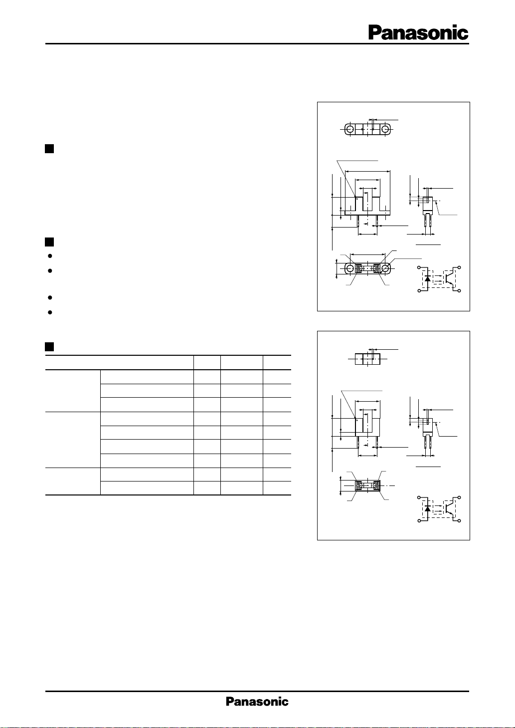
CNZ1111
0.45±0.1
Unit : mm
Overview
CNZ1111 and CNZ1112 are a photocoupler in which a high
efficiency GaAs infrared light emitting diode is used as the light
emitting element, and a high sensitivity phototransistor is used as
the light detecting element. The two elements are arranged so as to
face each other, and objects passing between them are detected.
Features
Highly precise position detection : 0.3 mm
Wide gap between emitting and detecting elements, suitable for
thick plate detection
Fast response : tr, tf = 6 µs (typ.)
Small output current variation against change in temperature
Absolute Maximum Ratings (Ta = 25˚C)
Parameter
Input (Light
emitting diode)
Reverse voltage (DC) V
Forward current (DC) I
Power dissipation P
Collector current I
Output (Photo
transistor)
Collector to emitter voltage
Emitter to collector voltage
Collector power dissipation
Temperature
*1
Input power derating ratio is 1.0 mW/˚C at Ta ≥ 25˚C.
*2
Output power derating ratio is 1.33 mW/˚C at Ta ≥ 25˚C.
Operating ambient temperature
Storage temperature T
Symbol
R
F
*1
D
C
V
CEO
V
ECO
*2
P
C
T
opr
stg
Ratings Unit
3V
50 mA
75 mW
20 mA
30 V
5V
100 mW
–25 to +85 ˚C
–30 to +100
˚C
Mark for indicating
LED side
25.0±0.35
13.0±0.3
5.0±0.2
A
10.0±0.2
2.5±0.2
A'
2-0.45±0.2
(10.0) (2.54)
6.0 min.
19.0±0.2
2
6.2±0.2
14
(Note) ( ) Dimension is reference
CNZ1112
Mark for indicating
LED side
13.0±0.3
5.0±0.2
A
10.0±0.2
2.5±0.2
A'
(10.0) (2.54)
2
6.0 min.
6.2±0.2
1
(Note) ( ) Dimension is reference
3
2-ø3.2±0.2
0.45±0.1
2-0.45±0.2
3
4
0.45±0.1
2.0±0.2
2.2±0.2
Device
center
SEC. A-A'
23
14
Pin connection
Unit : mm
0.45±0.1
2.0±0.2
2.2±0.2
Device
center
SEC. A-A'
23
14
Pin connection
1
Transmissive Photosensors (Photo Interrupters) CNZ1111,CNZ1112
Electrical Characteristics (Ta = 25˚C)
Parameter
Input
characteristics
Output
characteristics
Transfer
characteristics
*
Switching time measurement circuit
Forward voltage (DC) VFIF = 50mA 1.2 1.5 V
Reverse current (DC) IRVR = 3V 10 µA
Collector cutoff current I
Collector to emitter capacitance
Collector current ICV
Response time tr , t
Collector to emitter saturation voltage
Symbol
CEOVCE
CCV
*
f
V
CE(sat)IF
Conditions min typ max Unit
= 10V 200 nA
= 10V, f = 1MHz 5 pF
CE
= 10V, IF = 20mA 0.3 mA
CE
V
= 10V, IC = 1mA, RL = 100Ω
CC
6 µs
= 50mA, IC = 0.1mA 0.3 V
Sig.IN
50Ω R
IF , I
60
(mA)
C
50
, I
F
40
30
C
I
F
V
CC
Sig.OUT 10%
L
— Ta
(Input pulse)
(Output pulse)
(mA)
F
t
d
t
r
60
50
40
30
I
t
f
F
td : Delay time
: Rise time (Time required for the collector current to increase
t
90%
r
from 10% to 90% of its final value)
: Fall time (Time required for the collector current to decrease
t
f
from 90% to 10% of its initial value)
— V
F
Ta = 25˚C
10
(mA)
C
–1
10
I
— I
C
F
VCE = 10V
Ta = 25˚C
1
I
20
10
Forward current, collector current I
C
0
0 20406080100
– 25
Ambient temperature Ta (˚C )
2
20
Forward current I
10
0
0.4 0.8 1.2 1.6 2.42.0
0
Forward voltage VF (V)
–2
10
Collector current I
–3
10
–1
10
Forward current IF (mA)
11010
2
 Loading...