

Panasonic CNZ1023, CNZ1022, CNZ1021 Datasheet
Transmissive Photosensors (Photo Interrupters)
CNZ1021,CNZ1022,CNZ1023,CNA1009
Photo Interrupters
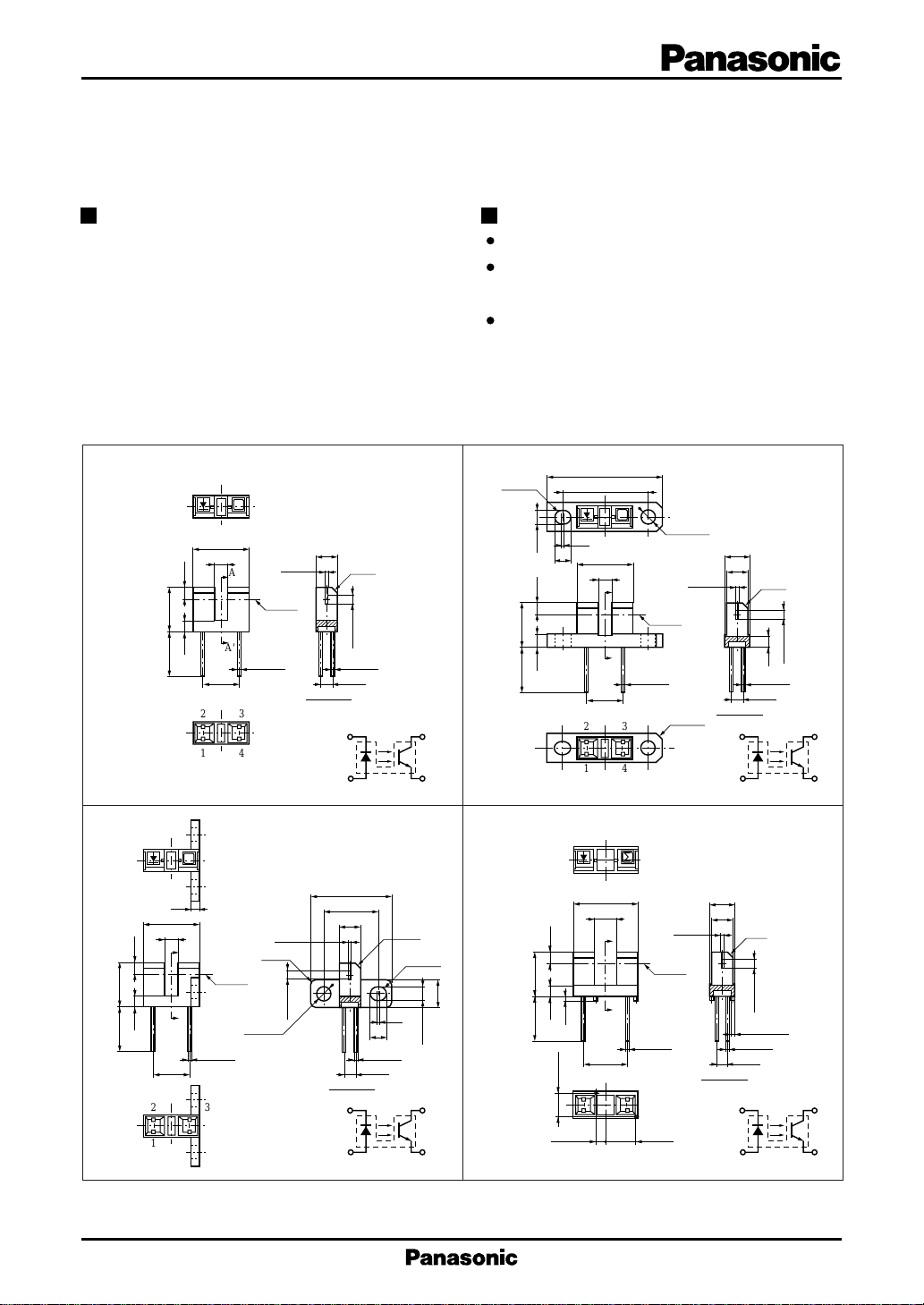
Overview
CNZ1021 series is a transmissive photosensor series
in which a high efficiency GaAs infrared light emitting
Features
Position detection accuracy : 0.25 mm
Gap width : 3 mm (CNZ1021, CNZ1022, CNZ1023)
diode is used as the light emitting element, and a high
sensitivity phototransistor is used as the light detecting
element. The two elements are arranged so as to face
each other, and objects passing between them are
detected.
The type directly attached to PCB........... CNZ1021
Screw-fastened type (both sides)............. CNZ1022
Screw-fastened type (one side)................ CNZ1023
The type directly attached to PCB........... CNA1009
(with a positioning pins)
CNZ1021 CNZ1022
∑
12.0
3.0±0.15
A
(2.5)
10.0
A'
2.5
10.0 min.
(2-0.45) (2-0.45)
(7.6) (2.54)
23
14
Device
0.4±0.1
center
5.0
(C1.2)
2.1±0.15
SEC. A-A'
23
14
CNZ1023
Unit : mm Unit : mm
2-R1.5
Pin connection
Unit : mm
CNA1009
+0.15
–0
3.0
(2.5)
10.0
3.0
10.0 min.
5 mm (CNA1009)
25.0
19.0±0.15
∑
0.5
3.5
12.0
3.0±0.15
A
A'
(2-0.45) (2-0.45)
(7.6)
23
14
Device
center
ø3.0
0.4±0.1
(2-C1.2)
+0.15
–0
6.0
5.0
(C1.2)
2.1±0.15
2.5
(2.54)
SEC. A-A'
23
14
Pin connection
Unit : mm
∑
2.0
12.0
3.0±0.15
A
(2.5)
10.0
2.5
10.0 min.
23
14
Device
center
A'
(2-0.45)
(7.6) (2.54)
ø3.0
0.4±0.1
(4-R2)
+0.15
–0
2.1±0.15
18.0
12.0±0.15
5.0
(C1.2)
2-R1.5
6.0
0.5
+0.15
–0
3.5
3.0
(2-0.45)
SEC. A-A'
23
14
Pin connection
∑
(2.5)2.5
10.0
10.0 min.
5.2±0.1
14.0
5.0±0.15
A
A'
2-0.7
(10.0)
23
14
Device
(2-0.45)
6.6±0.12.35±0.1
center
0.5±0.1
6.0
5.0
(C1)
2.2±0.15
2-ø0.7±0.1
(2-0.45)
(2.54)
SEC. A-A'
23
14
Pin connection
(Note) 1. Tolerance unless otherwise specified is ±0.3.
2. ( ) Dimension is reference.
1
Transmissive Photosensors (Photo Interrupters)
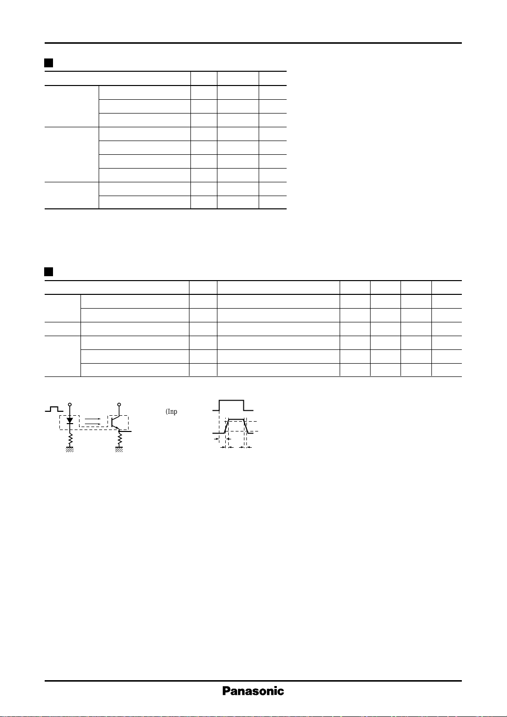
Absolute Maximum Ratings (Ta = 25˚C)
Parameter
Input (Light
emitting diode)
Reverse voltage (DC) V
Forward current (DC) I
Power dissipation P
Collector current I
Output (Photo
transistor)
Collector to emitter voltage
Emitter to collector voltage
Collector power dissipation
Temperature
*1
Input power derating ratio is 1.0 mW/˚C at Ta ≥ 25˚C.
*2
Output power derating ratio is 1.33 mW/˚C at Ta ≥ 25˚C.
Operating ambient temperature
Storage temperature T
Electrical Characteristics (Ta = 25˚C)
Parameter
Input
characteristics
Output characteristics
Transfer
characteristics
*
Switching time measurement circuit
Forward voltage (DC) VFIF = 20mA 1.25 1.4 V
Reverse current (DC) IRVR = 3V 10 µA
Collector cutoff current I
Collector current ICV
Collector to emitter saturation voltage
Response time tr , t
Symbol
R
F
*1
D
C
V
CEO
V
ECO
*2
P
C
T
opr
stg
Symbol
CEOVCE
V
CE(sat)IF
*
f
Ratings Unit
5V
50 mA
75 mW
20 mA
30 V
5V
100 mW
–25 to +85 ˚C
–40 to +100
˚C
Conditions min typ max Unit
= 10V 10 200 nA
= 5V, IF = 20mA, RL = 100Ω
CC
= 40mA, IC = 1mA 0.4 V
V
= 5V, IC = 1mA, RL = 100Ω
CC
CNZ1021,CNZ1022,CNZ1023,CNA1009
0.5 15 mA
5 µs
Sig.IN
50Ω R
V
CC
Sig.OUT 10%
L
(Input pulse)
(Output pulse)
t
d
t
r
td : Delay time
: Rise time (Time required for the collector current to increase
t
90%
r
from 10% to 90% of its final value)
: Fall time (Time required for the collector current to decrease
t
t
f
f
from 90% to 10% of its initial value)
2
 Loading...