

Panasonic AY-NE2000E Service Manual
SPECIFICATIONS
Video
Video Input
[Analogue]
Input Connectors: 2 sources (selectable from Composite. Y/C, Y/PB/PR)
Composite: 1.0 V[p-p]/75 Ω (BNC)
Y /C: Y: 1.0V[p-p]/75 Ω
C: 0.3 V[p-p]/75 Ω (Y/C terminal)
Component: Y: 1.0V[p-p]/75 Ω (BNC)
P
B/PR
: 0.525V[p-p] or 0.7V[p-p]/75 Ω (BNC) (75% Colour Bar)
[SDI (Option)]
SMPTE259M 75 Ω (BNC) with active loop-through
Video Output
[Analogue]
Output Connector: 2 outputs (simultaneously from Composite, Y/C, Y/PB/PR)
Composite: 1.0V[p-p]/75 Ω
Y/C: Y: 1.0V[p-p]/75 Ω
C: 0.3V[p-p]/75 Ω (Y/C terminal)
Component: Y: 1.0V[p-p]/75 Ω (BNC)
P
B/PR
: 0.525V[p-p] or 0.7V[p-p]/75 Ω (BNC) (75% Colour Bar)
[SDI (Option)]
SMPTE259M 75 Ω (BNC)
Synchronization
Gen-Lock Input: 1.0V[p-p]/75 Ω (BNC), with loop-through output (x1)
ADV.REF output: Sync: 0.3V[p-p]/75 Ω
Burst: 0.3V[p-p]/75 Ω
Nonlinear Workstation Main Kit
AY-NE2000E
ORDER NO. BSD9903011C8
C 1999 Matsushita Communication Industrial Co., Ltd.
All rights reserved. Unauthorized copying and
distribution is a violation of law.
This service information is designed for experienced repair technicians only and is not designed for use by the
general public.
It does not contain warnings or cautions to advise non-technical individuals of potential dangers in attempting to
service a product.
Products powered by electricity should be serviced or repaired only by experienced professional technicians. Any
attempt to service or repair the product or products dealt with in this service information by anyone else could
result in serious injury or death.
Y
WARNING
CAUTION
RISK OF ELECTRIC SHOCK
DO NOT OPEN
CAUTION:
TO REDUCE THE RISK OF ELECTRIC SHOCK,
DO NOT REMOVE COVER (OR BACK). NO USER
SERVICEABLE PARTS INSIDE.
REFER SERVICING TO QUALIFIED SERVICE
PERSONNEL.
This symbol warns the user that uninsulated voltage within
the unit may have sufficient magnitude to cause electric
shock. Therefore, it is dangerous to make any kind of contact
with any inside part of this unit.
This symbol alerts the user that important literature concerning
the operation and maintenance of this has been included.
Therefore, it should be read carefully in order to avoid
any problems.
There are special components used in this equipment which are important for safety. These parts are indicated
by the ”
Y ” mark on the schematic diagram and the replacement parts list. It is essential that these critical
parts should be replaced with manufacturer's specified parts to prevent X-radiation, shock, fire, or other hazards.
Do not modify the original design without permission of manufacture.
IMPORTANT SAFETY NOTICE
Audio Input
[Analogue]
Selectable from 4 sources
Source 1/2: +4dBu, 0dBu, –20dBu selectable, Hi-Z balanced (3-pin XLR connector)
Source 3/4: –6dBs, 20 kΩ, unbalanced (RCA pin jack)
[AES/EBU (Option)]
SMPTE279M 75 Ω (BNC)
Audio Output
[Analogue]
4 outputs (simultaneous)
Ch. 1/2: +4dBu, 0dBu, –20dBu selectable, 47 Ω balanced (3-pin XLR connector)
Ch. 3/4: –6dBs, 75 Ω, unbalanced (RCA pin jack)
[AES/EBU (Option)]
SMPTE279M 75 Ω (BNC)
Other Inputs/Outputs
LTC time code Input: x1 (BNC)
LTC time code output: x1 (BNC)
SCSI connector: x4 (Audio, Video 1, Video 2, Video 3, SCSI-2 standard,
68-pin half pitch connector, pin type)
VTR control connector : RS-422, 9 pin x2 (D-sub)
Jog Pad connector: 9 pin x1 (D-sub)
PC
CPU : Pentium Processor, MMX 200 MHz
OS : Windows 95
Main Memory : 32 MB DIMM 168-pin SDRAM
Built-in Hard Disk Drive : 3.2 GB (E-IDE) x1
Floppy Disk Drive : 1.44MB x1
ZIP Drive : 100MB x1
CD-ROM Drive : x32 Speed
Card Slot : PCI x3 (supplied by Panasonic only)

SVGA connector : 15 pinx1 (D-Shell, female),
1024 x 768 dots, 256 colours,
Scanning: 48 kHz (horizontal),
60 Hz (vertical)
Parallel connector : 25 pin x1 (D-Shell, female)
Serial connector : 9 pin x2 (D-Shell, male)
Mouse : 6 pin x1 (Mini-Din, female)
Keyboard : 6 pin x1 (MIni-Din, female)
Video Performance
S/N Ratio * : 55 dB (Y/PB/PR), 53 dB (Y/C), 50 dB (Composite)
DG, DP * : 5%, 3°
Frequency Response * : 4.5 MHz, +0dB, –3dB (Y/C, Y/P
B/PR
)
Sampling Frequency : 13.5 MHz, 4:2:2, 8 bit component
Y/C Separation : 3 lines, digital logical comb filter
SC-H : ±30°
Compression : MOTION JPEG
Compression Quality : Q3, Q6, Q8, Q11, Q23
Recording Time : Approx. 3 min/GB (Q3)
Approx. 6 min/GB (Q6)
Approx. 7 min/GB (Q8)
Approx. 10 min/GB (Q11)
Approx. 15 min/GB (Q23)
Title Graphics
Resolution : 640 x 480 dots Y, U, V, α, 8 bit component each
Font : True type
Audio Performance
S/N Ratio : More than 67 dB (1 kHz, XLR OUT)
Dynamic Range : More than 85 dB
Total Harmonic Distortion : 0.05% (1 kHz)
Frequency Response : 20 kHz, +0, –3 dB, 20 Hz, +0, –3 dB
Sampling Frequency : 48 kHz, 16 bit
Mixing : Stereo 4 channels
Effector : EQ, Reverberation
Recording Time : Approx. 86 min/GB
Others
EDL Output : CMX3600, CMX340, GVG, BVE9000, AU-A950 Format
Graphic Conversion : TIFF, JPEG, TARGA, BMP, WMF, PCT
General
Power Supply : 220 ~ 240V AC, 50 Hz
Power Consumption : 135W (with optional Video Board)
Ambient Operating Temperature : 0°C ~ 35°C (32°F ~ 95°F)
Ambient Operating Humidity : 10% ~ 90%
Weight : Main unit: 27.0 kg (59.5 Ibs)
Jog pad: 1.2 kg (2.6 Ibs)
Dimensions :
Main unit (W x H x D) : 420 x 319 x 461 mm
Jog pad (W x H x D) : 340 x 45 x 193 mm
Weight and dimensions indicated above are approximate.
Specifications are subject to change without notice.
This product might be subject, to export control regulations.
* : Without Compression

Nonlinear Editing System Digital I/F Board AY-PB2002E
Video
Input Signal: Comply with the SMPTE259M standards,
BNC x 1 (with active loop-through)
Output Signal:
Comply with the SMPTE259M standards, BNC x 1
Audio
Input Signal:
Comply with the AES/EBU standards, BNC x 1
Output Signal:
Comply with the AES/EBU standards, BNC x 1
General
Power Supply: 5V DC, 12V, –12V
Ambient Operating Temperature: 5°C to 35°C
Ambient Operating Humidity: 10% to 90%
Dimensions (W x H x D): 236 x 35.5 x 67 mm
Weight: Approx. 340 g

CONTENTS
Major Operating Controls And Their Functions . . . . . . . . . . . . . . . . . . . . . . . . . . . . . . . . . . . . . . . . . . . . . . . . . . . . 1
Adjustment Procedure . . . . . . . . . . . . . . . . . . . . . . . . . . . . . . . . . . . . . . . . . . . . . . . . . . . . . . . . . . . . . . . . . . . . . . . . 6
Location Of Test Points And Adjusting Controls . . . . . . . . . . . . . . . . . . . . . . . . . . . . . . . . . . . . . . . . . . . . . . . . . .14
Block Diagram
Input Board (1/2) . . . . . . . . . . . . . . . . . . . . . . . . . . . . . . . . . . . . . . . . . . . . . . . . . . . . . . . . . . . . . . . . . . . . . . . . . . .15
Input Board (2/2) . . . . . . . . . . . . . . . . . . . . . . . . . . . . . . . . . . . . . . . . . . . . . . . . . . . . . . . . . . . . . . . . . . . . . . . . . . .16
JPEG/SCSI Board (SCSI Section) . . . . . . . . . . . . . . . . . . . . . . . . . . . . . . . . . . . . . . . . . . . . . . . . . . . . . . . . . . . . . .17
JPEG/SCSI Board (JPEG Section) . . . . . . . . . . . . . . . . . . . . . . . . . . . . . . . . . . . . . . . . . . . . . . . . . . . . . . . . . . . . .18
Audio Board . . . . . . . . . . . . . . . . . . . . . . . . . . . . . . . . . . . . . . . . . . . . . . . . . . . . . . . . . . . . . . . . . . . . . . . . . . . . . . .19
CG Board . . . . . . . . . . . . . . . . . . . . . . . . . . . . . . . . . . . . . . . . . . . . . . . . . . . . . . . . . . . . . . . . . . . . . . . . . . . . . . . . .20
Mixer Board (1/4) . . . . . . . . . . . . . . . . . . . . . . . . . . . . . . . . . . . . . . . . . . . . . . . . . . . . . . . . . . . . . . . . . . . . . . . . . . .21
Mixer Board (2/4) . . . . . . . . . . . . . . . . . . . . . . . . . . . . . . . . . . . . . . . . . . . . . . . . . . . . . . . . . . . . . . . . . . . . . . . . . . .22
Mixer Board (3/4) . . . . . . . . . . . . . . . . . . . . . . . . . . . . . . . . . . . . . . . . . . . . . . . . . . . . . . . . . . . . . . . . . . . . . . . . . . .23
Mixer Board (4/4) . . . . . . . . . . . . . . . . . . . . . . . . . . . . . . . . . . . . . . . . . . . . . . . . . . . . . . . . . . . . . . . . . . . . . . . . . . .24
AY-PB2002E . . . . . . . . . . . . . . . . . . . . . . . . . . . . . . . . . . . . . . . . . . . . . . . . . . . . . . . . . . . . . . . . . . . . . . . . . . . . . .25
Schematic Diagram
JPEG/SCSI Board (JPEG Section) (1/2) . . . . . . . . . . . . . . . . . . . . . . . . . . . . . . . . . . . . . . . . . . . . . . . . . . . . . . . . .26
JPEG/SCSI Board (JPEG Section) (2/2) . . . . . . . . . . . . . . . . . . . . . . . . . . . . . . . . . . . . . . . . . . . . . . . . . . . . . . . . .27
JPEG/SCSI Board (SCSI Section) . . . . . . . . . . . . . . . . . . . . . . . . . . . . . . . . . . . . . . . . . . . . . . . . . . . . . . . . . . . . . .30
Input Board . . . . . . . . . . . . . . . . . . . . . . . . . . . . . . . . . . . . . . . . . . . . . . . . . . . . . . . . . . . . . . . . . . . . . . . . . . . . . . . .31
Mixer Board (1/3) . . . . . . . . . . . . . . . . . . . . . . . . . . . . . . . . . . . . . . . . . . . . . . . . . . . . . . . . . . . . . . . . . . . . . . . . . . .34
Mixer Board (2/3) . . . . . . . . . . . . . . . . . . . . . . . . . . . . . . . . . . . . . . . . . . . . . . . . . . . . . . . . . . . . . . . . . . . . . . . . . . .35
Mixer Board (3/3) . . . . . . . . . . . . . . . . . . . . . . . . . . . . . . . . . . . . . . . . . . . . . . . . . . . . . . . . . . . . . . . . . . . . . . . . . . .36
CG Board . . . . . . . . . . . . . . . . . . . . . . . . . . . . . . . . . . . . . . . . . . . . . . . . . . . . . . . . . . . . . . . . . . . . . . . . . . . . . . . . .37
AY-PB2002E . . . . . . . . . . . . . . . . . . . . . . . . . . . . . . . . . . . . . . . . . . . . . . . . . . . . . . . . . . . . . . . . . . . . . . . . . . . . . .39
PCI Interface Board . . . . . . . . . . . . . . . . . . . . . . . . . . . . . . . . . . . . . . . . . . . . . . . . . . . . . . . . . . . . . . . . . . . . . . . . .42
Power Board/Power Switch Board/LED Board . . . . . . . . . . . . . . . . . . . . . . . . . . . . . . . . . . . . . . . . . . . . . . . . . . . .43
Mother Board (1/2) . . . . . . . . . . . . . . . . . . . . . . . . . . . . . . . . . . . . . . . . . . . . . . . . . . . . . . . . . . . . . . . . . . . . . . . . . .46
Mother Board (2/2) . . . . . . . . . . . . . . . . . . . . . . . . . . . . . . . . . . . . . . . . . . . . . . . . . . . . . . . . . . . . . . . . . . . . . . . . . .47
Audio Board (1/2) . . . . . . . . . . . . . . . . . . . . . . . . . . . . . . . . . . . . . . . . . . . . . . . . . . . . . . . . . . . . . . . . . . . . . . . . . . .48
Audio Board (2/2) . . . . . . . . . . . . . . . . . . . . . . . . . . . . . . . . . . . . . . . . . . . . . . . . . . . . . . . . . . . . . . . . . . . . . . . . . . .49
Rear Board-1 . . . . . . . . . . . . . . . . . . . . . . . . . . . . . . . . . . . . . . . . . . . . . . . . . . . . . . . . . . . . . . . . . . . . . . . . . . . . . .51
Rear Board-3 . . . . . . . . . . . . . . . . . . . . . . . . . . . . . . . . . . . . . . . . . . . . . . . . . . . . . . . . . . . . . . . . . . . . . . . . . . . . . .52
Conductor View
JPEG/SCSI Board (JPEG Section) . . . . . . . . . . . . . . . . . . . . . . . . . . . . . . . . . . . . . . . . . . . . . . . . . . . . . . . . . . . . .28
JPEG/SCSI Board (SCSI Section) . . . . . . . . . . . . . . . . . . . . . . . . . . . . . . . . . . . . . . . . . . . . . . . . . . . . . . . . . . . . . .29
Input Board . . . . . . . . . . . . . . . . . . . . . . . . . . . . . . . . . . . . . . . . . . . . . . . . . . . . . . . . . . . . . . . . . . . . . . . . . . . . . . . .32
Mixer Board . . . . . . . . . . . . . . . . . . . . . . . . . . . . . . . . . . . . . . . . . . . . . . . . . . . . . . . . . . . . . . . . . . . . . . . . . . . . . . .33
CG Board . . . . . . . . . . . . . . . . . . . . . . . . . . . . . . . . . . . . . . . . . . . . . . . . . . . . . . . . . . . . . . . . . . . . . . . . . . . . . . . . .38
AY-PB2002E . . . . . . . . . . . . . . . . . . . . . . . . . . . . . . . . . . . . . . . . . . . . . . . . . . . . . . . . . . . . . . . . . . . . . . . . . . . . . .40
PCI Interface Board . . . . . . . . . . . . . . . . . . . . . . . . . . . . . . . . . . . . . . . . . . . . . . . . . . . . . . . . . . . . . . . . . . . . . . . . .41
Power Board/Power Switch Board/LED Board . . . . . . . . . . . . . . . . . . . . . . . . . . . . . . . . . . . . . . . . . . . . . . . . . . . .44
Mother Board . . . . . . . . . . . . . . . . . . . . . . . . . . . . . . . . . . . . . . . . . . . . . . . . . . . . . . . . . . . . . . . . . . . . . . . . . . . . . .45
Audio Board . . . . . . . . . . . . . . . . . . . . . . . . . . . . . . . . . . . . . . . . . . . . . . . . . . . . . . . . . . . . . . . . . . . . . . . . . . . . . . .50
Rear Board-1 . . . . . . . . . . . . . . . . . . . . . . . . . . . . . . . . . . . . . . . . . . . . . . . . . . . . . . . . . . . . . . . . . . . . . . . . . . . . . .51
Rear Board-3 . . . . . . . . . . . . . . . . . . . . . . . . . . . . . . . . . . . . . . . . . . . . . . . . . . . . . . . . . . . . . . . . . . . . . . . . . . . . . .52
Exploded View
AY-NE2000E . . . . . . . . . . . . . . . . . . . . . . . . . . . . . . . . . . . . . . . . . . . . . . . . . . . . . . . . . . . . . . . . . . . . . . . . . . . . . .53
AY-PB2002E . . . . . . . . . . . . . . . . . . . . . . . . . . . . . . . . . . . . . . . . . . . . . . . . . . . . . . . . . . . . . . . . . . . . . . . . . . . . . .54
Replacement Parts List . . . . . . . . . . . . . . . . . . . . . . . . . . . . . . . . . . . . . . . . . . . . . . . . . . . . . . . . . . . . . . . . . . . . . . .55
1
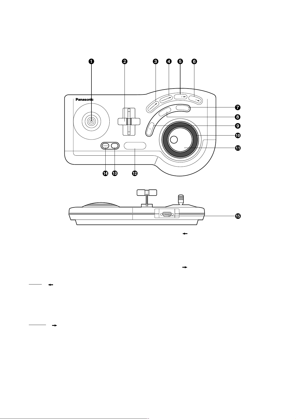
MAJOR OPERATING CONTROLS AND THEIR FUNCTION
■ FRONT PANEL
1. Power On/Off Switch
Turns the power of this unit on and off.
Notes:
1. Be sure to turn on the power of this unit after turning
on the Hard Disk Box.
2. Do not turn off the power of this unit while the
Nonlinear AV Workstation System software is running.
2. Power Indicator (RED)
Lights by turning on the power.
3. HDD Indicator (GREEN)
Lights up while the HDD operates.
4. 3.5” Floppy Disk Drive
5. Floppy Disk Indicator/Eject Button
Indicator.......Lights during an access of the floppy disk.
Eject button..Ejects the Floppy Disk.
6. Front Panel
Caution: Do not interrupt the Vent Hole on this panel.
7. ZIP Drive
8. ZIP Indicator/Eject Button
Lights during an access of the ZIP.
Ejects the ZIP.
9. CD-ROM Drive
10. CD-ROM Indicator/Eject Button
Indicator.......Lights during an access of the
CD-ROM.
Eject button..Ejects the CD-ROM.
2
AC IN
IN1
IN2
LR
RL
OUT1
OUT2
AUDIO
OUT
LR
OUT1
LR
OUT2
BALANCED
AUDIO OUT
L
IN1 IN2
BALANCED
AUDIO IN
LRR
CONTROL 1 CONTROL 2 JOG PAD
Y/C
COMPOSITE
Y
P
B PR
IN1
IN2
G/L IN
LOOP
75Ω
Y/C COMPOSITE Y P
B PR
ADV REF
OUT
OUT1
OUT2
TC IN
VIDEO
IN
AUTO
VIDEO
OUT
TC OUT
AUDIO
IN
SEE MANUAL
KB MOUSE SEPIAL 1
SEPIAL 2 PRINTER
S-VGA
SCSI AUDIO SCSI VIDEO 1 SCSI VIDEO 2 SCSI VIDEO 3
VIDEO(DIGITAL)
IN
OUT
AUDIO(AES/EBU)
IN OUT
VIDEO(DIGITAL)
IN
OUT
AUDIO(AES/EBU)
IN OUT
~
■ REAR PANEL
11. KEYBOARD Connector (KB)
Connects with the keyboard (locally purchase).
If the cable is too short to connect, use the Key Board
Extension Cable (accessory).
12. MOUSE Connector (MOUSE)
Connects with the Mouse (locally purchase).
When the cable is too short to connect, use the Mouse
Extension Cable (accessory).
13. PRINTER Connector (PRINTER)
Connects with the printer.
14. SERIAL1/2 Connectors (SERIAL 1/SERIAL 2)
Connects with equipment having RS-232C Interface
Connectors.
15. PCI Slots
Refer to qualified service personnel.
16. S-VGA Connector (S-VGA)
Connects with the computer display.
The applicable display parameters are shown below.
Resolution: 1024 x 768
Horizontal Scanning Frequency: 48 kHz
Vertical Scanning Frequency: 60 Hz
17. Fan
Supplies steady forced air through intake and filter.
Note: After extensive use the fans need to be replaced
periodically.
18. SDI Board Slots
Operating Time Operating Life
8-hour everyday use 6-year
12-hour everyday use 4-year
24-hour everyday use 2-year

3
19. SCSI VIDEO Connectors (SCSI VIDEO 1-3)
Connects with the SCSI Video Connector of the Hard
Disk Box AY-EB2000 or WJ-EB1000 via the optional
SCSI Cable AY-CA68SR3 for AY-EB2000 or
AY-CA50SR3 for WJ-EB1000.
20. TC (Time Code) IN Connector (TC IN)
Connects with a VTR having LTC time code signal
output connector to improve editing accuracy.
21. TC (Time Code) OUT Connector (TC OUT)
Connects with a VTR having LTC time code signal input
connector.
The signal supplied from this connector is not looped
through.
22. AC Inlet
Connect the AC Power Cord (provided).
23. AUDIO OUT 1/2 Jacks
(AUDIO OUT OUT1, OUT2 L/R)
Supply the audio signals.
24. ADV-REF OUT Connector (ADV-REF OUT)
Supplies the Advance Reference Signal to the VTR
having the time base corrector inside (or AUX video
source).
25. Video Output Connectors
(VIDEO OUT1/OUT2 Y/C, COMPOSITE, Y, P
B
, PR)
Supplies the video signal to the monitor or VTR.
26. AUDIO OUT 1/2 Connectors
(BALANCED AUDIO OUT, OUT1/OUT2)
Supply the audio signals.
27. G/L IN / AUTO Connectors (G/L, IN/AUTO)
The gen-lock signal is supplied to these connectors (Be
sure to terminate the video signal output from these
connectors).
By connecting with the G/L AUTO Connector, the video
signal is automatically unterminated.
Caution:
If a gen-lock signal is supplied to the G/L connector
during playback or recording, it may cause the video
to roll or cause other system malfunction.
Stop the playback or recording, then make a
connection to the G/L connector again.
28. AUDIO IN 1/2 Jacks (IN1, IN2 L/R) (Unbalanced)
Accepts the audio signal.
The audio signal supplied to these jacks can be saved in
the Hard Disk Box.
When the audio signal is supplied to the L side only, a
monaural audio signal is made.
29. AUDIO IN 1/2 Connectors
(BALANCED AUDIO IN IN1 L/R, IN2 L/R)
Accepts the audio signal.
The audio signal supplied to these connectors can be
saved in the Hard Disk Box.
30. Video 1/2 Input Connectors
(VIDEO IN1/IN2 Y/C, COMPOSITE, Y, P
B
, PR)
Accepts the video signals to be saved in the Hard Disk
Box.
Select the connector, either Composite, Y/C or
Component, according to the type of video signal.
The selection of either Video 1/Video 2 is available on
the PC monitor screen.
31. CONTROL 1/2 Connectors
(CONTROL 1/CONTROL 2) (9-pin)
Supplies the control signal (for the recording or play
back mode) to equipment having an RS-422 Interface
Connector.
Be sure to supply the video signal of the VTR connected
with CONTROL 1 to VIDEO IN 1, and likewise with the
VTR connected to CONTROL 2.
32. JOGPAD Connector (JOGPAD)
Connects with the Jogpad (provided).
33. SCSI AUDIO Connector (SCSI AUDIO)
Supplies the audio signal to the SCSI Audio Connector
of the optional Hard Disk Box via the optional SCSI
Cable AY-CA68SR3 for AY-EB2000 or AY-CA50SR3 for
WJ-EB1000.
4
OPEN
OK
UNDO SHIFT
TRIM
MODE
DIVIDE
DELETE
ZOOM
G
OTO
PLAY STOP
MARK IN
M
A
R
K
O
UT
■ JOG PAD
1. Positioner
Moves the selection cursor (when selection is
confirmed).
2. Wipe Lever
Controls Wipe, Key Size, and Audio Level.
3. TRIM
/
MODE
Switches edit modes (Insert - Replace - Cover)
(SHIFT + TRIM/MODE)
Turns Trim mode On/Off. (during transition)
4. DIVIDE
/
DELETE
Deletes a clip.
(SHIFT + DIVIDE / DELETE)
Divides a clip.
5. ZOOM /
Zooms in the time line.
(SHIFT + ZOOM)
Zooms out the time line.
6. GOTO /
Jumps to the starting or editing mark.
(SHIFT + GOTO)
Jumps to the beginning or end of a sequence.
7. MARK OUT
Sets or cancels the ending mark.
(SHIFT + MARK OUT)
Selects the grip of the OUT point.

5
8. MARK IN
Sets or cancels the starting mark.
(SHIFT + MARK IN)
Selects the grip of the IN point.
9. PLAY/STOP
Plays back or stops.
(SHIFT + PLAY /STOP)
Plays back between the starting and ending marks.
10. Shuttle Ring
Plays back video and audio forward (clockwise) or in
reverse (counterclockwise) with variable speed.
11. Jog Dial
Plays back video and audio forward (clockwise) or in
reverse (counterclockwise) frame by frame.
12. SHIFT
Switches button functions.
13. UNDO
Cancels the immediately previous operation.
14. OPEN
OK
Opens the selected panel or selects a panel and closes
the previous panel.
15. Jog Pad Connector
Connects with the Main Unit by using the Jog Pad Cable
(accessory).
6
ADJUSTMENT PROCEDURE
1. Test Equipment Required
8
The following test Equipments are required for
adjustment of the Nonlinear AV Workstation Main Kit
AY-NE2000E.
8
Oscilloscope
8
Frequency Counter
8
Digital Voltmeter
8
Waveform Monitor
8
Vectorscope (with SC-H Function)
8
Underscanned Colour Video Monitor
8
Test Signal Generator (Colour Bar signal, Ramp signal
and etc.)
8
Extension Board (YWVOEA0356AN) for AY-NE2000E
2. Disassembling Procedure for
Adjustment
■ AY-NE2000E
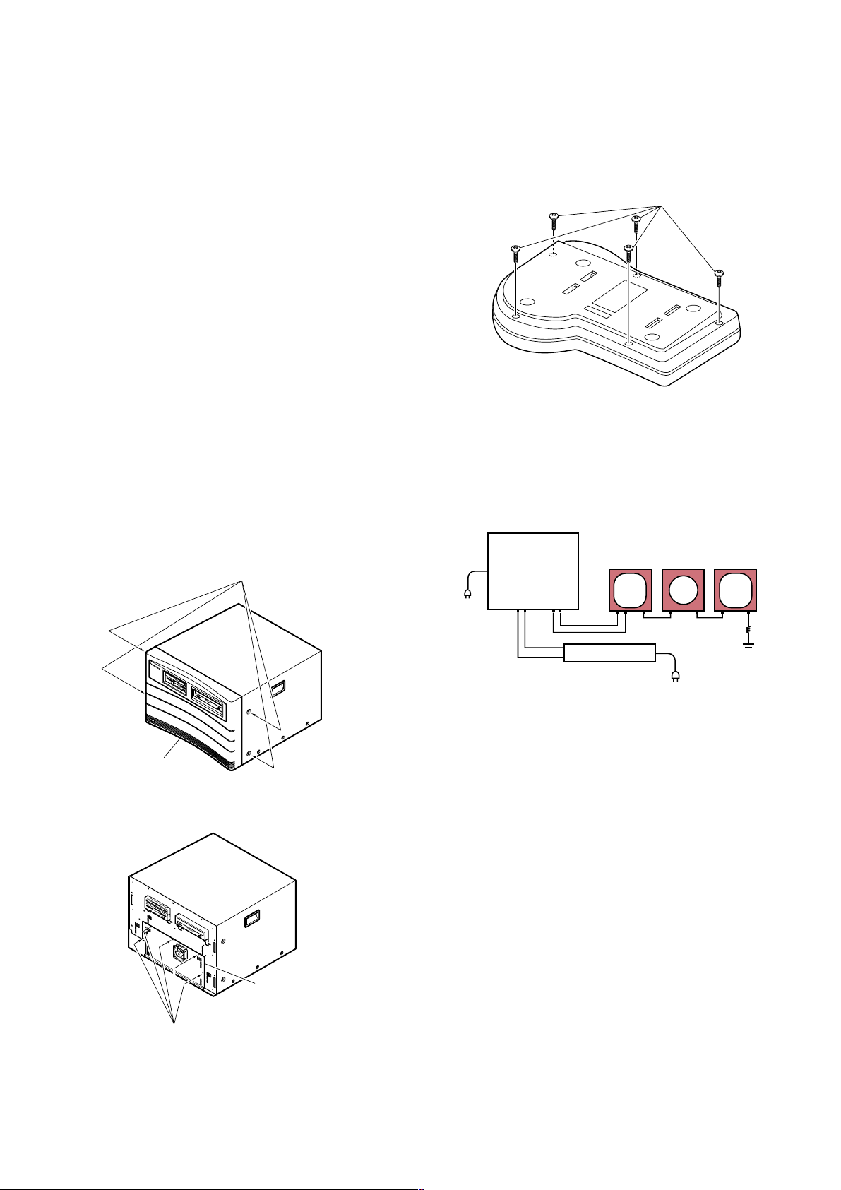
Referring to Fig. 2-1, rremove four screws that secure the
Front Panel and remove the Front Panel.
Fig. 2-1
8
Referring to Fig.2-2, remove five screws fixing the Front
Chassis and remove the Front Chassis.
Fig. 2-2
■ Jog Pad
8
Referring to Fig. 2-3, remove five screws that secure the
Bottom Cover and remove the Bottom Cover.
Fig. 2-3
3. Connection for Adjustment
8
The Fig. 3-1 shows the connection diagram for the
adjustment procedure.
Fig. 3-1
8
Connect the Underscanned Color Video Monitor through
the Waveform Monitor and Vectorscope to either Y/C
Video Output Connector or Composite Video Output
Connector on the Rear Panel of the AY-NE2000E.
8
Terminate the input terminal of the Underscanned Colour
Video Monitor with 75 Ω.
8
Connect the probe of the Digital Voltmeter, Oscilloscope
or Frequency Counter at the desired Test Point in each
adjustment step.
8
The adjustment should be done after 10 minutes warm-up.
Remove four screws.
Front Panel
AY-NE2000E
Waveform
Monitor
Vectorscope
Underscanned
Colour Video
Monitor
75
Ω
Signal Generator
Remove five screws.
Remove five screws.
Front Chassis

7
4. Adjustment Procedure
8
Refer to the Location of the Test Points and
Adjusting Controls on page 14.
■ Power Board
(1). Power Good Signal Adjustment
Test Point: Pin 2 of CN3 (5V) Power Board
Pin 1 of CN3 (P-GOOD) Power Board
Adjust: VR1 (4.85V) Power Board
VR3 (P-GOOD) Power Board
8
Connect the Digital Voltmeter to the pin 2 of CN3.
8
Adjust VR1 to obtain 4.85 ± 0.5 V DC.
8
Change the connection of the Digital Voltmeter to the pin 1
of CN3.
8
Adjust VR3 so that the Power Good Signal level just
changes from Low level to High level.
8
Confirm that the changing point should be between 4.8V
DC and 4.9V DC by adjusting of VR1.
(2). 5V Adjustment
Test Point: L202 (5V) Mixer Board
Adjust: VR1 (5V) Power Board
8
Connect the Digital Voltmeter to L202 on the Mixer Board.
8
Adjust VR1 to obtain 5.05 ± 0.02V DC.
(3). 12V Adjustment
Test Point: TP3 (12V) Mixer Board
Adjust: VR2 (12V) Power Board
8
Connect the Digital Voltmeter to TP3 on the Mixer Board.
8
Adjust VR2 to obtain 12 ± 0.05V DC.
■ Mixer Board
(4). Subcarrier Frequency Adjustment
Test Point: TP6 (FSC) Mixer Board
Adjust: VR202 (FSC) Mixer Board
8
Connect the Frequency Counter to TP6.
8
Adjust VR202 to obtain 17.734525 MHz ± 5 Hz.
(5). Ach VCO Adjustment
Test Point: Land between R997 and L742 (Ach VCO)
Mixer Board
Adjust: L742 (Ach VCO) Mixer Board
8
Executes the Manual Digitizer and set the Record mode.
8
Select the CH1-Y/C Input by the Device setting, and
supply the Colour Bar signal to the Y/C Video Input
Connector of CH1.
8
Connect the Digital Voltmeter to the land between R997
and L742.
8
Adjust L742 to obtain 2.1 ± 0.1V DC.
(6). Bch VCO Adjustment
Test Point: Land between R98 and L743 (Bch VCO)
Mixer Board
Adjust: L743 (Bch VCO) Mixer Board
8
Set the SW1 and SW2 on the Pattern Side of the MIxer
Board are as shown in Fig. 3-1.
Fig. 3-1
8
Executes the Manual Digitizer and set the Record mode.
8
Select the CH1-Y/C Input by the Device setting, and
supply the Colour Bar signal to the Y/C Video Input
Connector of CH1.
8
Connect the Digital Voltmeter to the land between R98
and L743.
8
Adjust L743 to obtain 2.1 ± 0.1V DC.
8
After completion of adjustment, set the SW1 and SW2 as
shown in Fig. 3-2.
Fig. 3-2
■ Before start to next steps, executes the Sequence
Editor, then plays the Still Image of the Colour Bar
(Setup = 0) by drag & drop the Colour Bar Icon to the
Sequence Editor.
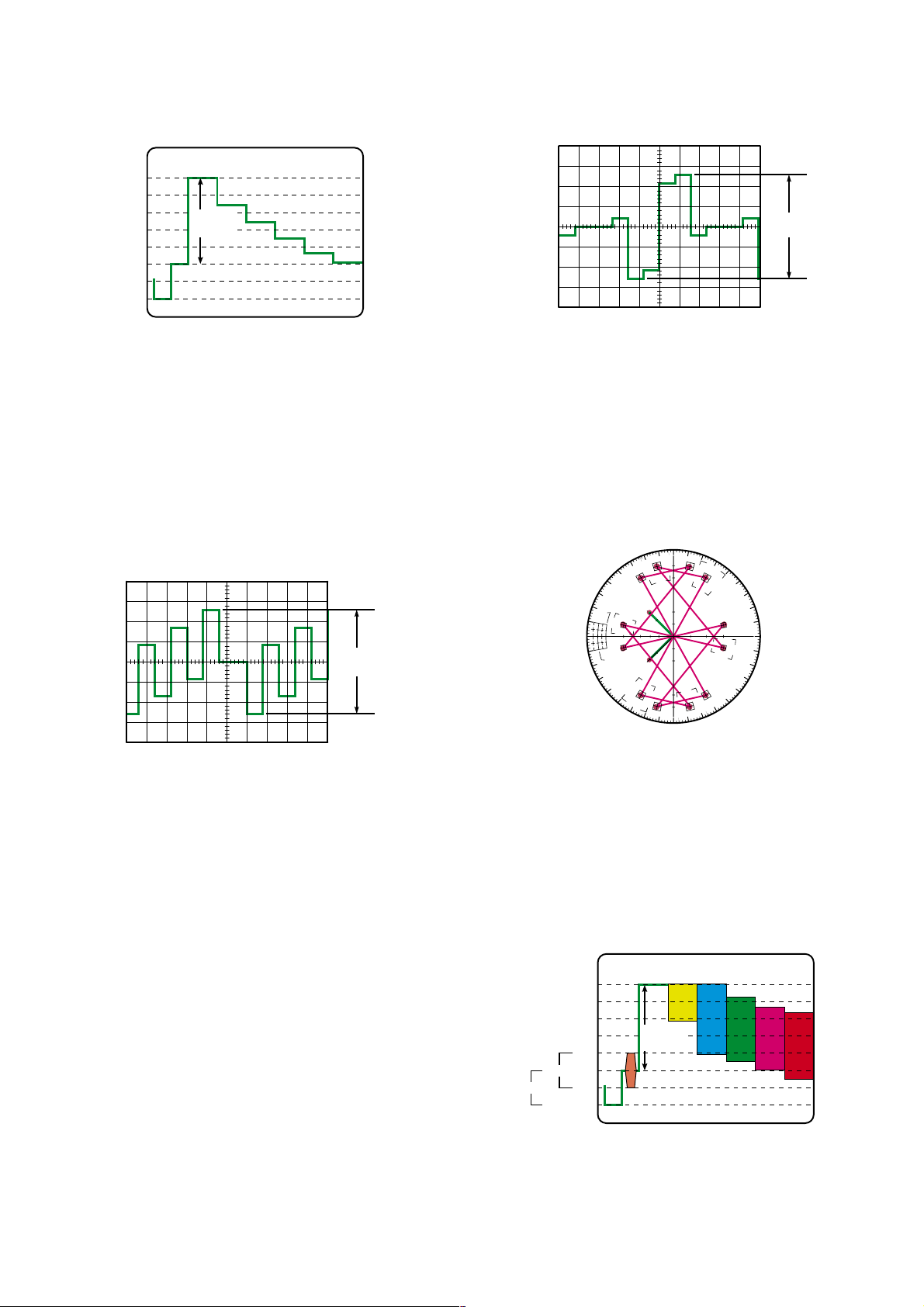
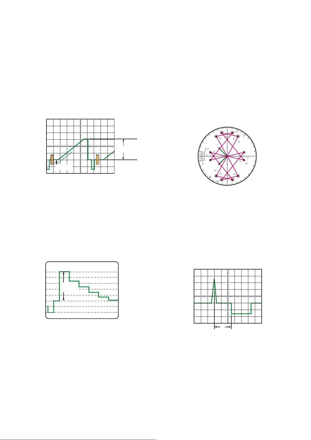
(7). Output Y Gain Adjustment
Test Point: Video Out Y Connector Rear Panel
Adjust: R439 (Y GAIN) Mixer Board
8
Connect the Waveform Monitor to the Video Out Y
Connector.
8
Adjust R439 so that the Y Level of the Y Reference signal
becomes 700 ± 7 mV as shown in Fig. 3-3.
ONON
8
7 6 5 4 3 2 1 8 7 6 5 4 3 2 1
SW1 SW2
ONON
8
7 6 5 4 3 2 1 8 7 6 5 4 3 2 1
SW1 SW2
8
Fig. 3-3
(8). Output PB Gain Adjustment
Test Point: Video Out PB Connector Rear Panel
Adjust: R442 (P
B GAIN) Mixer Board
8
Set the Video Out to MII Component by the Device
Setting.
8
Connect the terminated Oscilloscope with 75Ω to the
Video Out P
B Connector.
8
Adjust VR442 so that the PB signal level of the build-in
Colour Bar signal (Setup = 0) becomes 525 mV as shown
in Fig. 3-4.
Fig. 3-4
Note: When using the β Component for the adjustment,
adjust it to 756 mV (106 ± 1 IRE).
(9). Output PR Gain Adjustment
Test Point: Video Out PR Connector Rear Panel
Adjust: R443 (P
R GAIN) Mixer Board
8
Set the Video Out to MII Component by the Device
Setting.
8
Connect the terminated Oscilloscope with 75Ω to the
Video Out P
R Connector.
8
Adjust R443 so that the PR signal level (p-p) of the build-in
Colour Bar signal (Setup = 0) becomes 525 mV as shown
in Fig. 3-5.
100
20
–20
–40
700 ± 7
mV
Fig. 3-5
Note: When using the β Component for the adjustment,
adjust it to 756 mV (106 ± 1 IRE).
(10). Output C Gain Adjustment
Test Point: Video Out Y/C Connector Rear Panel
Adjust: R441 (C GAIN) Mixer Board
8
Connect the Vectorscope to the Video Out Y/C Connector.
8
Adjust VR441 so that the Chrominance Gain and Phase
are adjusted to proper position (± 3%, 3%) as shown in
Fig. 3-6.
Fig. 3-6
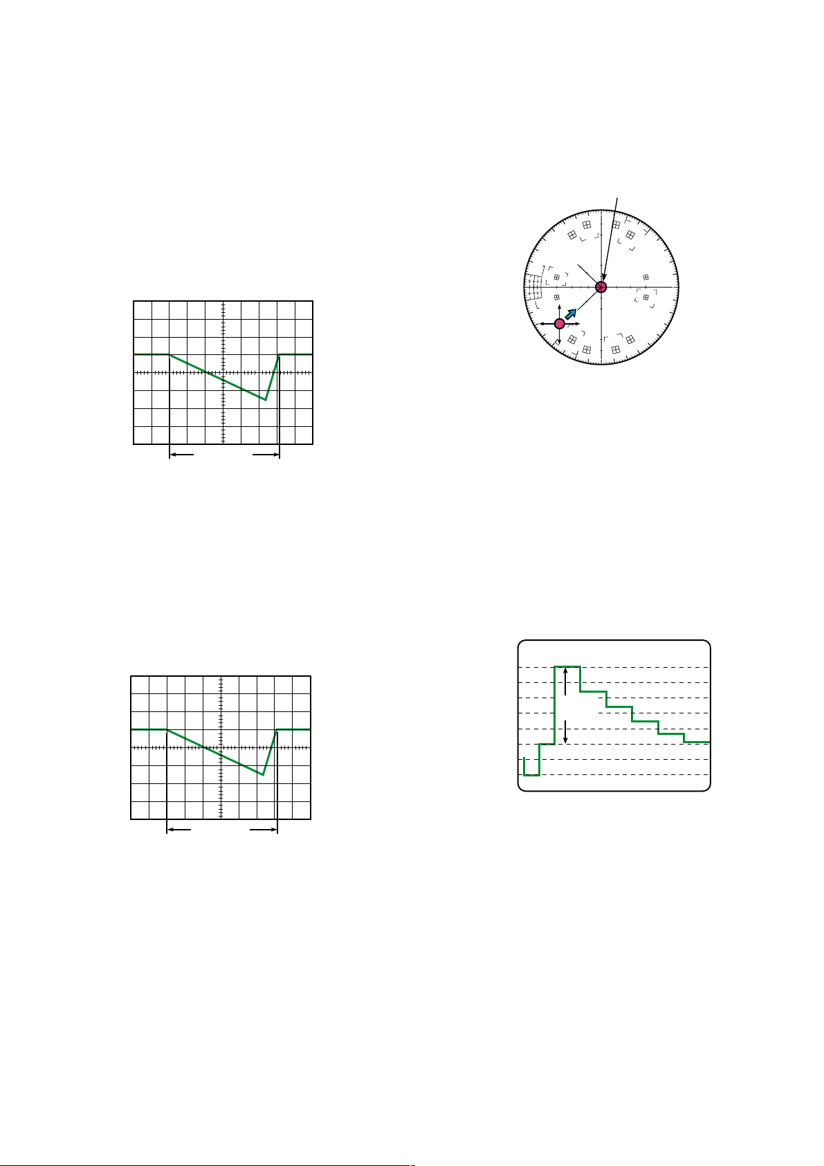
(11). Composite Y Gain Adjustment
Test Point: Video Out Composite Connector
Rear Panel
Adjust: R440 (COMP Y) Mixer Board
8
Connect the Waveform Monitor to the Video Out
Composite Connector.
8
Adjust VR440 so that the Y signal level becomes 700 ± 7
mV as shown in Fig. 3-7.
Fig. 3-7
525 mV
525 mV
cy
g
MG
YL
yl
B
b
G
C
Y
dG
10°
0°
10°
dø
100%
75%
R
V
U
mg
r
20%
20%
dG
100
20
–20
–40
BURST
SYNC
700 ± 7
mV
9
(12). Output C Gain Adjustment
Test Point: Video Out Composite Connector
Rear Panel
Adjust: R444 (COMP C) Mixer Board
8
Connect the Vectorscope to the Video Out Y/C Connector.
8
Adjust R444 so that the Chrominance Gain and Phase are
adjusted to proper position (± 3%, 3%) as shown in Fig. 3-
8.
Fig. 3-8
(13). Output SC-H Adjustment
Test Point: Video Out Composite Connector
Rear Panel
Adjust: R445 (SC-H) Mixer Board
8
Connect the Vectorscope to the Video Out Y/C Connector.
8
Adjust R445 so that the SC-H Phase becomes 0 ± 5°.
(14). ADV. REF. SC-H Adjustment
Test Point: ADV. REF. Out Connector Rear Panel
Adjust: R446 (ADV.REF.) Mixer Board
8
Connect the Vectorscope to the ADV. REF. Output
Connector.
8
Adjust R446 so that the SC-H Phase becomes 0 ± 5°.
(15). Gen/Lock Colour Phase Adjustment
Test Point: Video Out Composite Connector
Rear Panel
Adjust: R438 (C-PHASE) Mixer Board
8
Supply the Video signal to the Gen/Lock Input Connector.
8
Adjust the Colour Phase roughly 0° by Switch SW201.
8
Adjust R438 so that the Colour Phase becomes 0 ± 10 °.
(16). Gen/Lock Horizontal Phase Adjustment
Test Point: Video Out Composite Connector
Rear Panel
Adjust: R436 (H-PHASE) Mixer Board
8
Supply the Video signal to the Gen/Lock Input Connector.
8
Adjust the Horizontal Phase roughly 0° by Switch SW203.
8
Adjust the Horizontal Phase 0° by Switch SW202.
8
Adjust R436 so that the Horizontal Phase becomes 0 ± 70
nS.
■ Input Board
■ Before start to adjust the Input Board, executes the
executes Manual Digitizer, set the Record mode.
(17). FVCXO1 Frequency Adjustment
Test Point: TP202 (FVCXO1) Input Board
Adjust: C601 (FVCXO1) Input Board
8
Disconnect all input from the AY-NE2000E.
8
Connect the Frequency Counter to TP202.
8
Adjust C601 to obtain 4.433624 MHz ± 5 Hz.
(18). FVCXO2 Frequency Adjustment
Test Point: TP206 (FVCXO2) Input Board
Adjust: C602 (FVCXO2) Input Board
8
Disconnect all input from the AY-NE2000E.
8
Connect the Frequency Counter to TP206.
8
Adjust C602 to obtain 4.433624 MHz ± 5 Hz.
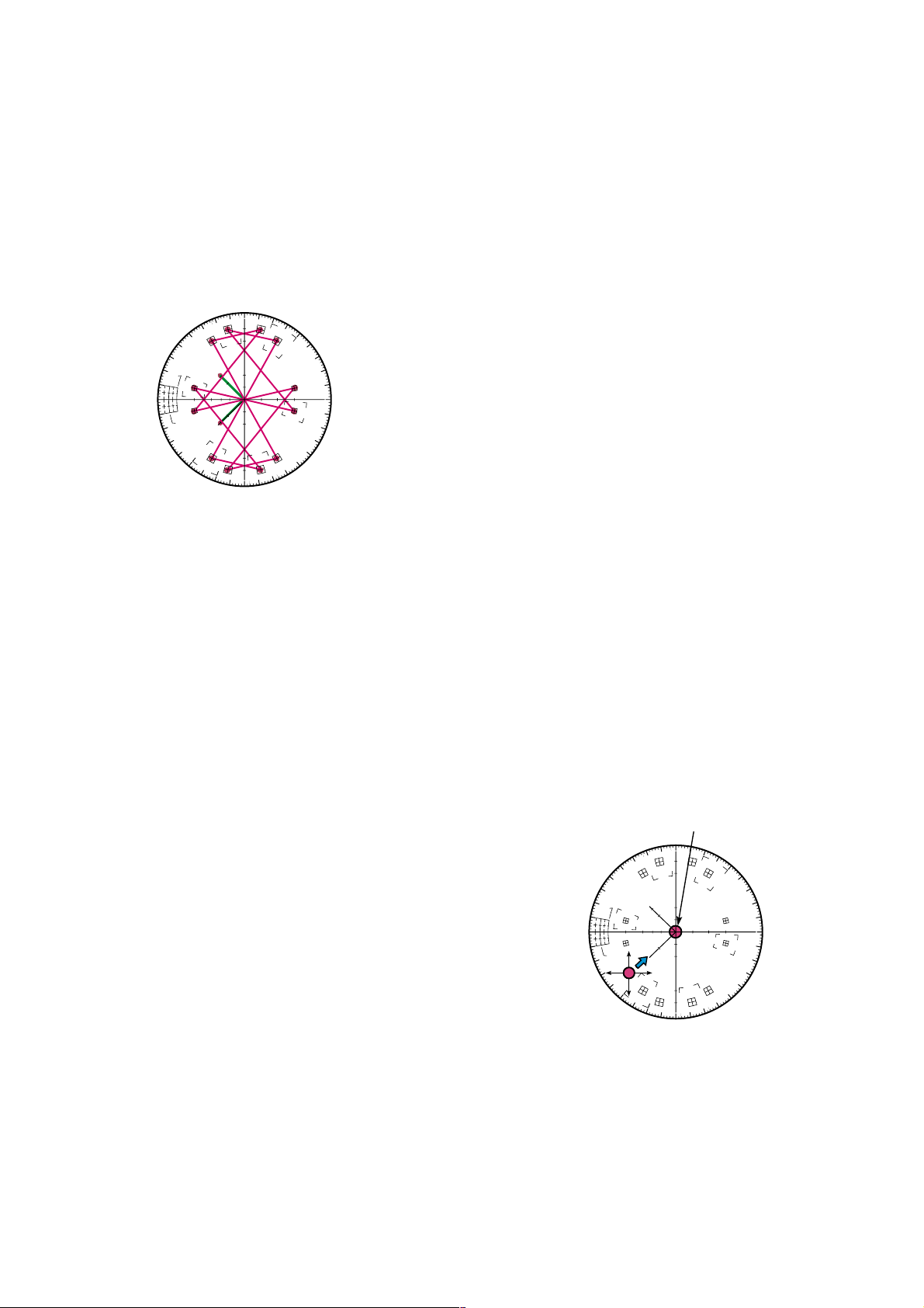
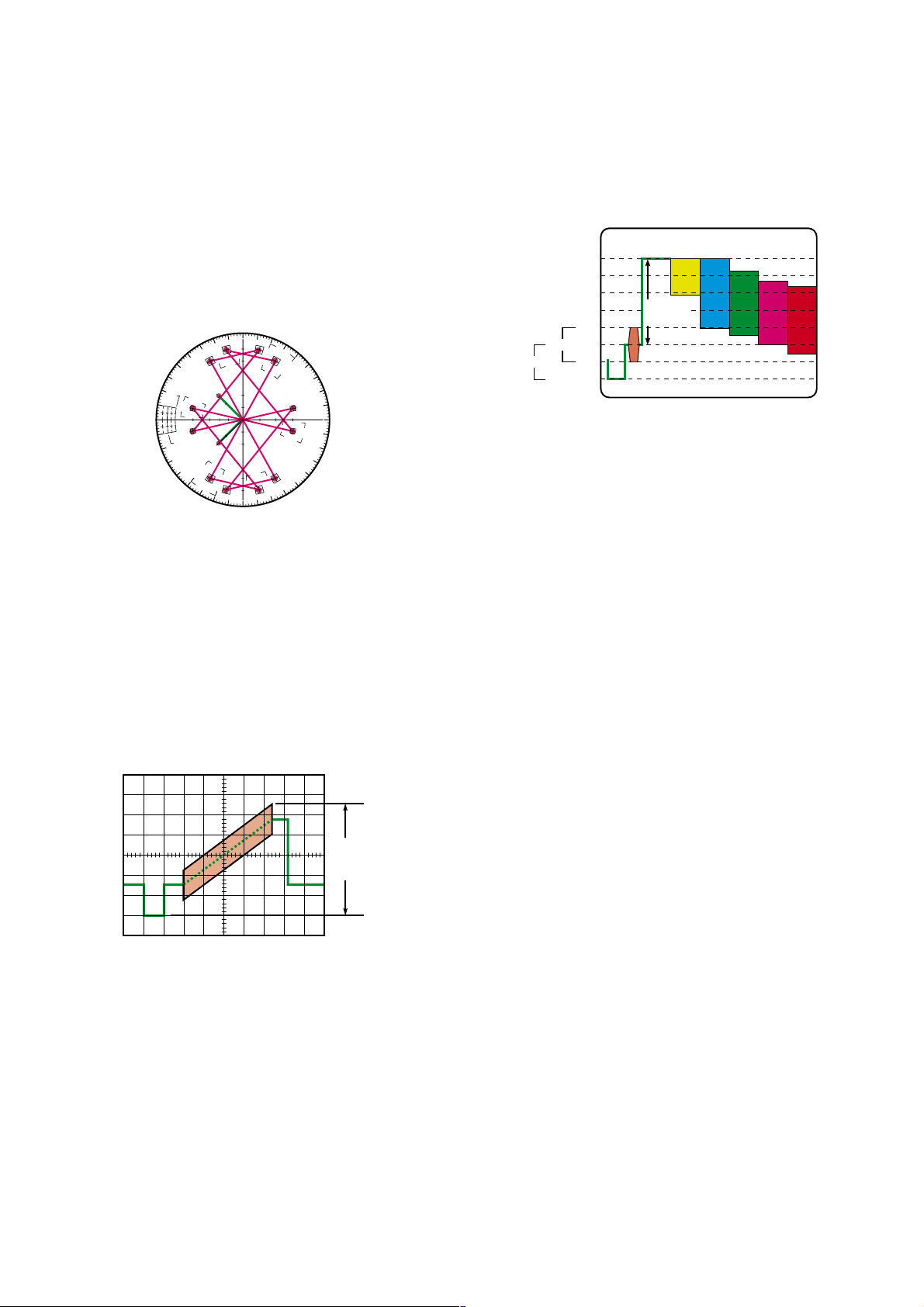
(19). Component Carrier Balance Adjustment
Test Point: Video Out Y/C Connector Rear Panel
Adjust: R805 (COMP CAR BAL-1) Input Board
R806 (COMP CAR BAL-2) Input Board
8
Select the CH1-Component Input by the Device setting,
and supply the Colour Bar signal to the Component Input
Connector of CH1.
8
Connect the Vectorscope to the Video Out Y/C Connector.
8
Set the Gain Control of the Vectorscope to the maximum.
8
Adjust R805 and R806 so that the vector positions at the
center of the Vectorscope as shown in Fig. 3-9.
Fig. 3-9
8
Set the Gain Control of the Vectorscope to the normal.
cy
g
MG
YL
yl
B
b
G
C
Y
dG
10°
0°
10°
dø
100%
75%
R
V
U
mg
r
20%
20%
dG
Positions at center.
cy
g
MG
YL
yl
B
b
G
C
Y
dG
10°
0°
10°
dø
100%
75%
R
V
U
mg
r
20%
20%
dG
10
(20). Pedestal Level Adjustment
Test Point: Video Out Y/C Connector Rear Panel
Adjust: R812 (PED) Input Board
8
Select the CH1-Component Input by the Device setting,
and supply the Ramp signal to the Component Input
Connector of CH1.
8
Connect the Terminated Oscilloscope with 75Ω to the
Video Out Y/C Connector.
8
Adjust R812 so that the Pedestal signal level becomes 0
IRE as shown in Fig. 3-10.
Fig. 3-10
(21). Component Y Gain Adjustment
Test Point: Video Out Y/C Connector Rear Panel
Adjust: R811 (COMP Y GAIN) Input Board
8
Select the CH1-Component Input by the Device setting,
and supply the Ramp signal to the Component Input
Connector of CH1.
8
Connect the Waveform Monitor to the Video Out Y/C
Connector.
8
Adjust R811 so that the Y signal level becomes 700 ± 1 4
mV as shown in Fig. 3-11.
Fig. 3-11
8
Confirm that the Pedestal level stays same level,
8
If not,
repeat steps 20 and 21 until satisfactory.
+ 1
– 0
700 ± 7 mV
NG
0 mV
+ 7
– 0
(22). Component C Gain Adjustment
Test Point: Video Out Y/C Connector Rear Panel
Adjust: R809 (COMP C GAIN-1) Input Board
R810 (COMP C GAIN-2) Input Board
8
Select the β Component Input by the Device setting, and
supply the P
B = 0.7V Component Colour Bar signal to the
Component Input Connector of CH1.
8
Connect the Vectorscope to the Video Out Y/C Connector.
8
Adjust R809 and R810 so that the Chrominance Gain and
Phase are adjusted to proper position (± 3%, 3%) as
shown in Fig. 3-12.
Fig. 3-12
(23). Horizontal Phase Adjustment
Test Point: Video Out Y/C Connector Rear Panel
Adjust: R804 (H-PHASE) Input Board
8
Select the CH1-Y/C Input by the Device setting, and
supply the Cross-hatch signal to the Y/C Video Input
Connector of CH1.
8
Connect the Oscilloscope to the Video Output terminal of
the Signal Generator, then measure the Horizontal Phase
” t ” as shown in the Fig. 3-13.
Fig. 3-13
8
Change the connection of the Oscilloscope to the Y
terminal of the Video Out Y/C Connector.
8
Adjust R804 so that the Horizontal Phase becomes t ± 70
nS.
cy
g
MG
YL
yl
B
b
G
C
Y
dG
10°
0°
10°
dø
100%
75%
R
V
U
mg
r
20%
20%
dG
100
20
–20
–40
700 ± 14
mV
t
11
(24). Burst Gate Pulse Width 1 Adjustment
Test Point: TP211 (BGP-1) Input Board
Adjust: R794 (BGP-1) Input Board
8
Select the CH1-Composite Input by the Device setting,
and supply the Colour Bar signal to the Composite Video
Input Connector of CH1.
8
Connect the Oscilloscope to TP211.
8
Adjust R794 so that the Burst Gate Pulse Width becomes
8.4 µS as shown in Fig. 3-14.
Fig. 3-14
(25). Burst Gate Pulse Width 2 Adjustment
Test Point: TP205 (BGP-2) Input Board
Adjust: R799 (BGP-2) Input Board
8
Select the CH1-Y/C Input by the Device setting, and
supply the Colour Bar signal to the Y/C Video Input
Connector of CH1.
8
Connect the Oscilloscope to TP205.
8
Adjust R799 so that the Burst Gate Pulse Width becomes
8.4 µS as shown in Fig. 3-15.
Fig. 3-15
(26). Y/C Carrier Balance Adjustment
Test Point: Video Out Y/C Connector Rear Panel
Adjust: R807 (Y/C CAR BAL-1) Input Board
R808 (Y/C CAR BAL-2) Input Board
8
Select the CH1-Y/C Input by the Device setting, and
supply the Colour Bar signal to the Y/C Video Input
Connector of CH1.
8
Connect the Vectorscope to the Video Out Y/C Connector.
t = 8.4 µS
8
Set the Gain Control of the Vectorscope to the maximum.
8
Adjust R807 and R808 so that the vector positions at the
center of the Vectorscope as shown in Fig. 3-16.
Fig. 3-16
8
Set the Gain Control of the Vectorscope to the normal.
(27). Y/C Y Gain Adjustment
Test Point: Video Out Y/C Connector Rear Panel
Adjust: R797 (Y/C Y GAIN) Input Board
8
Select the CH1-Y/C Input by the Device setting, and
supply the Colour Bar signal to the Y/C Video Input
Connector of CH1.
8
Connect the Waveform Monitor to the Video Out Y/C
Connector.
8
Adjust R797 so that the Y signal level becomes 700 ± 7
mV as shown in Fig. 3-18.
Fig. 3-18
(28). Y/C Chrominance Adjustment
Test Point: Video Out Y/C Connector Rear Panel
Adjust: R800 (Y/C R-Y GAIN) Input Board
R802 (Y/C B-Y GAIN) Input Board
R801 (TINT) Input Board
8
Select the CH1-Y/C Input by the Device setting, and
supply the Colour Bar signal to the Y/C Video Input
Connector of CH1.
8
Connect the Waveform Monitor to the Video Out Y/C
Connector.
t = 8.4 µS
Positions at center.
cy
g
MG
YL
yl
B
b
G
C
Y
dG
10°
0°
10°
dø
100%
75%
R
V
U
mg
r
20%
20%
dG
100
20
–20
–40
700 ± 7
mV
12
8
Aim the Red vector, adjust R800 so that the Red vector
becomes proper position.
8
Aim the Yellow vector, adjust R802 so that the Yellow
vector becomes proper position.
8
Aim the Red vector, adjust R801 so that the Red vector
becomes proper position.
8
Repeat adjustment R800, R802 and R801 so that the
Chrominance Gain and Phase are adjusted to proper
position as shown in Fig. 3-19.
Fig. 3-19
(29). Y/C Separation Gain Adjustment
Test Point: Video Out Composite Connector
Rear Panel
Adjust: R793 (Y/C SEPA GAIN) Input Board
8
Select the CH1-Composite Input by the Device setting,
and supply the Ramp (Chroma 40 IRE (286 mV)) signal to
the Composite Input Connector of CH1.
8
Connect the Oscilloscope to TP201.
8
Adjust 793 so that the Y/C Separation signal becomes
maximum without saturation as shown in Fig. 3-20.
Fig. 3-20
(30). Composite Y Gain Adjustment
Test Point: Video Out Composite Connector
Rear Panel
Adjust: R798 (COMP Y-GAIN) Input Board
8
Select the CH1-Composite Input by the Device setting,
and supply the Colour Bar signal to the Composite Input
Connector of CH1.
cy
g
MG
YL
yl
B
b
G
C
Y
dG
10°
0°
10°
dø
100%
75%
R
V
U
mg
r
20%
20%
dG
8
Connect the Waveform Monitor to the Video Out Y/C
Connector.
8
Adjust R798 so that the Y signal level becomes 700 ± 7
mV as shown in Fig. 3-21.
Fig. 3-21
- Audio Board
(31). Balance Output Level Adjustment
Test Point: 1-CH Unbalanced Audio
Output Connector-L Rear Panel
1-CH Unbalanced Audio
Output Connector-R Rear Panel
Adjust: R759 (BAL-L) Audio Board
R762 (BAL-R) Audio Board
8
Supply 1 KHz Tone Clip to the Sequence Editor and
playback.
8
Connect the AC Voltmeter (with dB Measure) to the 1-CH
Balanced Audio Output Connector-L.
8
Adjust R759 so that the 1-CH Balanced Output level
becomes 0.00 ± 0.10 dBµ.
8
Change the connection of the AC Voltmeter (with dB
Measure) to the 1-CH Balanced Audio Output ConnectorR.
8
Adjust R762 so that the 1-CH Balanced Output level
becomes 0.00 ± 0.10 dBµ.
(32). Unbalance Output Level Adjustment
Test Point: 3-CH Unbalanced Audio
Output Connector-L Rear Panel
3-CH Unbalanced Audio
Output Connector-R Rear Panel
Adjust: R245 (UNBAL-L) Audio Board
R247 (UNBAL-R) Audio Board
8
Supply 1 KHz Tone Clip to the Sequence Editor and
playback.
8
Connect the AC Voltmeter (with dB Measure) to the 3-CH
Unbalanced Audio Output Connector-L.
Becomes maximum
without satiration
100
20
–20
–40
BURST
SYNC
700 ± 7
mV

13
■ Jog pad WJ-JP1000
■ Before start to adjust the Jog Pad, remove the
Bottom Cover, connect supplied cable between the
Jog Pad and AY-NE2000E.
(34). Wipe High Level Adjustment
Test Point: TP2 (WIPE H) Jog Pad Board
TP3 (WIPE L) Jog pad Board
Adjust: VR3 (WIPE H) Jog pad Board
8
Move the Wipe Level Controls and Audio Level Knob to +
side slightly.
8
Connect the Digital Voltmeter to TP3 and measure the
voltage at TP3 (this voltage is E).
8
Change the connection of the Digital Voltmeter to TP2.
8
Adjust VR3 so that the voltage at TP2 becomes E – (0.2 ±
0.05) V.
(35). Wipe Low Level Adjustment
Test Point: TP3 (WIPE L) Jog Pad Board
Adjust: VR4 (WIPE L) Jog pad Board
8
Move the Wipe Level Controls and Audio Level Knob to
the frontward slightly.
8
Connect the Digital Voltmeter to TP3.
8
Adjust VR4 to obtain –0.2 ± 0.05 V.
8
Adjust R245 so that the 3-CH Unbalanced Output level
becomes – 6.00 ± 0.10 dBs.
8
Change the connection of the AC Voltmeter (with dB
Measure) to the 3-CH Unbalanced Audio Output
Connector-R.
8
Adjust R247 so that the 3-CH Unbalanced Output level
becomes – 6.00 ± 0.10 dBs.
(33). Input Level Adjustment
Test Point: 1-CH Balanced Audio
Output Connector-L Rear Panel
1-CH Balanced Audio
Output Connector-R Rear Panel
Adjust: R263 (INPUT-L) Audio Board
R266 (INPUT-R) Audio Board
8
Supply 1 KHz (0.00 ± 0.10 dBµ) signal from the Audio
Analyzer to the 1-CH Balanced Input Connector-L.
8
Executes the Manual Digitizer and select 1-CH Balanced
Input Connector-L by the Device setting.
8
Connect the AC Voltmeter (with dB Measure) to the 1-CH
Balanced Audio Output Connector-L.
8
Adjust R263 so that the 1-CH Balanced Output level-L
becomes 0.00 ± 0.10 dBµ.
8
Supply 1 KHz (0.00 ± 0.10 dBµ) signal from the Audio
Analyzer to the 1-CH Balanced Input Connector-R.
8
Executes the Manual Digitizer and select 1-CH Balanced
Input Connector-R by the Device setting.
8
Change the connection of the AC Voltmeter (with dB
Measure) to the 1-CH Balanced Audio Output ConnectorR.
8
Adjust R266 so that the 1-CH Balanced Output level-R
becomes 0.00 ± 0.10 dBµ.
POWER BOARD (COMPONENT SIDE)
VR2
(12V)
VR1
(5V)
CN3-2
(5V)
CN3-1
(P-GOOD)
CN3
VR3
(WIPE H)
VR4 (WIPE L)
VR3
(P-GOOD)
CN2
WJ-JP1000
MAIN BOARD (PATTERN SIDE)
}{POIUYTREWQ
TP2 (WIPE H)
TP3 (WIPE L)
TP211
(BGP-1)
TP205
(BGP-2)
TP201
()
TP203 ()
TP202
(FVCXO1)
R795
()
R796
()
R794
(BGP-1)
R799 (BGP-2)
R800 (Y/C Y GAIN)
C602 (FVCXO2)
C601
(FVCXO1)
R801 (TINT)
R798
(COMP Y-GAIN)
R793
(Y/C SEPA GAIN)
R804
(H-PHASE)
R802 (Y/C B-Y GAIN)
R803
R811
(COMP Y GAIN)
R810 (COMP C GAIN-2)
R809 (COMP C GAIN-1)
R806 (COMP CAR BAL-2)
R812 (PED)
R805
(COMP CAR BAL-1)
R807
(Y/C CAR BAL-1)
R808
(Y/C CAR BAL-2)
TP219
()
TP206
(FVCXO2)
TP207
TP208 TP210
TP209
TP221
TP218
TP227
TP45
TP44
TP3 (12V)
L742
(Bch VCO)
R98
R977
L742 (Ach VCO)
L202 (5V)
TP11
TP4
TP6 (FSC)
R439 (Y GAIN)
R440 (COMP Y)
R444 (COMP C)
R441 (C GAIN)
R442 (P
B GAIN)
R443 (PR GAIN)
R446 (ADV.REF.)
TP14
TP2
TP1
R436
(H-PHASE)
TP5
SW201
SW202
SW203
R438
(FSC)
R445 (SC-H)
MIXER BOARD (COMPONENT SIDE)INPUT BOARD (COMPONENT SIDE)
R762 (BAL-R)
R247 (UNBAL-R)
R266 (INPUT-R)R263 (INPUT-L)
R245 (UNBAL-L)
R759 (BAL-L)
AUDIO BOARD (COMPONENT SIDE)
LOCATION OF TEST POINTS AND ADJUSTING CONTROLS
– 14 –
AO9AO8
+5V
+5V
+5V
+5V
+5V
4852566064
+5V
+5V
+5V
+5V
+5V
+5V
100
104
108
112
116
120
P1
P2
P11
+5VD
SF1
FL202
AMP
+5V
BIAS
R193
Q208
REFERENCE
VOLTAGE
GENERATOR
Q209,Q210,U201
19
17
23
1
7
VRB
VRT
VIN
D0|D7
67-74
IYC1|IYC8
U205
Y/C SEPARATOR
AMP FL208
OCIO
TP213
AMP
TP201
AMP FL206
OYIO
TP212
AMP
TP203
TP204
38
27
80 4 2
Q219,Q220
Q217,Q218
Q222
Q223
U204
U203
A/D
CONVERTER
3-10
AMP
AMP
AMP
FL201
Q201
AMP
AMP
AMP
55
C.SYNC
P2
P2
P2
P2
P2
P2
P2
TO
MOTHER
BOARD
TO
MOTHER
BOARD
TO
MOTHER
BOARDTOMOTHER
BOARD
TO
MOTHER
BOARD
TO
MOTHER
BOARD
TO
MOTHER
BOARD
TO
MOTHER
BOARD
TO
MOTHER
BOARDTOMOTHER
BOARDTOMOTHER
BOARD
TO
MOTHER
BOARD
TO
MOTHER
BOARD
TO
MOTHER
BOARD
TO
MOTHER
BOARD
TO
MOTHER
BOARD
P12
2
153
12
13
U210 SELECTOR
BUFFER
Y0Y1Z0Z1X0
X1
15
BUFFER4BUFFER
14
BUFFER
Q290
Q291
Q215
11
10
9
ABC
AO3
AMP
Q213
P2
P2
P2
P2
P2
11
10
9
ABC
AO3
AMP
AMP
AMP
AMP
BUFFER
Q292
Y
Z
X
Q211
15
BUFFER
Q293
4
WHD
151617
LD
CLK
DI
125
3
Y0Y1Z0
Z1
Y
Z
AO1
AO3
AO5
AO6
AO7
AO8
AO9
U211 SELECTOR
AO1
AO3
AO5
AO6
AO7
AO8
AO9
U224
D/A CONVERTER
18245678
B.P.F.
5
2
+5V
4
+5V
R794
R795
25
YIN
CIN
BF GW
GAIN
TINT
VCXOI
VCXO
OUT
11
+5V
R796
(TINT)
10
12
BUFFER
Q212
IGCK
C601
Y201
U202
CHROMA DIFFERENCE EDECODER
Q202-Q207
FL205
AMP
AMP
FL203 FL204 AMP
BIAS
Q216
Q284
Q285-Q287
Q281-Q283
U207 SWITCH
231
231
7
54
AO8
AMP
AO7
Q224 Q236
25
AMP
Q225 Q237
2
+5V
R799
4
+5V
R800
5
16
14
3
23
24
BLKIN
HDIN
CIN
RYIN
BYIN
COUT
YIN
BPGW
GAIN
SYNC
AMP
Q244- Q247
BIAS
Q252
AMP
Q248-Q251
19
28
11
+5V
R801
R802
10
12
C602 Y202
RYO
BYO
TINT
VCXOI
VCXO
OUT
WHD
1
2
4
U212
+5VD
+5VD
+5V
REGULATOR
+5V
REGULATOR
+5V
REGULATOR
+5V
+5V
+5V
1
1
1
+5V
REGULATOR
+5V
REGULATOR
+5V
REGULATOR
+5V
+5V
+5V
1
1
1
+12
U242
U217
U213
U245
U232
U243
BUFFER
BUFFER
BUFFER
BUFFER
Q238
Q243
Q239
Q242
+5V
3
2
+
-
1
+
-
7
5
6
+5V
3
2
+
-
1
+
-
7
5
6
R806
R805
R807
R808
U233 (2/ 4)
U233 (1/4)
U218(1/ 4)
U218(2 /4)
U206
SWITCH
7
U234 SELECTOR
13
12
1
2
14
15
X1X0Y1
Y0
Y
X
CBA
9
11
10
AO8
24
1
3
5
7
U220 SWITCH
Q254
AO9
AO8
24
1
3
5
7
U221 SWITCH
Q262
AO9AO8
24
1
3
5
7
U222 SWITCH
Q270
Q240
Q241
FL209
AMP
A01
A3 Y3
8
9
OE3
a
a
b
c
b
c
Q255
AMP
Q256-Q259
FL210
AMP
Q263
AMP
Q264-Q267
FL211
AMP
Q272-Q275
AMP
Q271
FL212
1
2
AO6
1
3
U244 SWITCH
+5V
AMP
Q294
7
3
U223
VCA
BIAS
10
9
+
-
8
U218 (3/ 4)
+5V
A05
R809
R810
R811
Q253
1
2
4
U215
R804
U216
1
2
4
Q226
Q227
Q228
Q229
Q230
Q231
Q232
Q233
Q234
Q235
3
3
3
3
3
3
R797
AMP
Q214
FL207
R812
U214
CHROMA DIFFERENCE
DECODER
20
1
COMP IN
COMP2
109COMP1
111
Y2
115
Y1
113
C1
117
C2
119
YCY IN
1
WHD 75
U1
U2
V2
V1
114
116
119
120
STRV
SCK
SDATA
119
111
115
P1
Q277
Q261
Q269
CLAMP
Q260
CLAMP
Q268
CLAMP
Q276
D4D5D6D7D0D1D2
D3
VIN
CLK
VRT
VRB
Q3Q2Q1Q0Q7Q6Q5
Q4
D3D2D1D0D7D6D5D4CP
U226
A/ D CONVERTER
U252
D-FFs
D4D5D6D7D0D1D2
D3
VIN
CLK
VRT
VRB
D7D6D5D4D3D2D1
D0
VIN
CLK
VRT
VRB
U235 A/ D CONVERTER
U229 A/ D CONVERTER
REFERENCE
VOLTAGE
GENERATOR
+5V
1
7
Q288,Q289, U219
A0B0A1B1A2B2A3
B3
D0D1D2D3D4D5D6D7CP
Q0Q1Q2Q3Q4Q5Q6
Q7
OE
Y7A
Y6A
Y5A
Y4A
Y3A
Y2A
Y1A
Y0A
73747778818285
86
C7A
C6A
C5A
C4A
C3A
C2A
C1A
C0A
8990939497
98
101
102
676371
59
CADCLK
YADCLK
CSEL
CLAMP
24
28
+12V
+12V
36
40
+12V
+12V
2345678
9
11
19181716151413
12
D0D1D2D3D4D5D6D7CP
Q0Q1Q2Q3Q4Q5Q6
Q7
OE
2345678
9
11
19181716151413
12
1297
4
A0B0A1B1A2B2A3
B3
Y3Y2Y1
Y0
1
1
2
1
10913
12
3
8
11
42
+5V
U239
U238
U230
D-FFs
U227
D-FFs
U236
2 1 SELECTOR
U237
2 1
SELECTOR
78910345
6
5432987
6
11
16171819121314
15
235
6
111014
13
78910345
6
235
6
111014
13
abcdefg
h
i
jkl
m
nop
aib
j
c
k
d
efg
h
l
m
nop
P2
P2
P2
+12V
SF201
TO INPUT BOARD (2/2)
+12V
+12V
+5VD+5VD
SF2
1297
4
P2
P1
Y3Y2Y1
Y0
191217
23
191217
23
191217
23
10987654
3
S
S
BLOCK DIAGRAM OF INPUT BOARD (1/2)
INUPT BOARD
1
3
P10
COMP IN
YCY IN
BUFFER
BUFFER
TP207
BUFFER
BUFFER
BUFFER
BUFFER
BUFFER
BUFFER
BUFFER
BUFFER
+5V
REGULATOR
+5V
REGULATOR
+5V
+5V
1
1
+12
U246
U247
3
3
TP208
TP209
TP210
U250(a)
BUS BUFFER
BUFFER
A01
1
A01
1
– 15 –
SDO
SDI
ISPEN
MODE
SCLK
23468
SD15
SD14
SD13
SD12
SD11
SD10
SD9
SD8
SD7
SD6
SD5
SD4
SD3
SD2
SD1
SD0
818283848586878889909192939495
96
P1
SA1
SA2
SA3
SA4
SA5
SA6
SA7
SA8
SA9
IOR
IOW
VP
797877757473717069
102
106
107
P1
TO
MOTHER
BOARD
TO
MOTHER
BOARD
P13
U1 LOGIC CONTROL
PSDO
PSCLK
SLATCH
SCS
PSDI
12569
135
131
IRQ10
IRQ11
IRQ10
IRQ11
IRQMX
IRQJ1
IRQJ2
IRQJ3
IRQCG
IRQA
CMDMX
CMDJ1
CMDJ2
CMDJ3
CMDA
2711151923314735394351
P2
P1
P1
P1
P1
131721
25
RXA1
RXB1
RXA2
RXB2
181426
22
TXB1
TXA1
TXB2
TXA2
P1
992933
HD
TCIN
TCOUT
Q0Q1Q2Q3Q4
Q5
D0D1D2D3D4
D5
1918171615
14
CMDMX
CMDJ1
CMDJ2
CMDJ3
CMDA
23456
7
Q0Q1Q2Q3Q4Q5Q6
D0D1D2D3D4D5D6
1918171615
14
IRQMX
IRQJ1
IRQJ2
IRQJ3
IRQCG
IRQA
2345678
IRQ10
IRQ11
U240 D-LATCH
U241 D-LATCH
13
18
8
7
30
21
SDO
SDI
ISPEN
MODE
SCLK
A0A1A2
WR
10-16,19,20
SA1|SA9
IOR
IOW
21
9
HD15
HD14
HD13
HD12
HD11
HD10
HD9
HD8
HD7
HD6
HD5
HD4
HD3
HD2
HD1
HD0
HD0-HD3
VP
22-25
HD0|HD3
RES
RST
HD0-HD15
D0D1D2
CK
Q0Q1Q2
U18 D-FFs U10 MICROPROCESSOR
U19 D-FFs
U21 TIME CODE
U30
Q2
Q1
U20
U9
VOLTAGE DETECTOR
4
5129
3611
234
A0A1A2
IRQR/W
NMI
FACK
PA6
NMIMASK
IRQ10
IRQ11
Q4Q3Q2Q1Q0
1516171819
IRQ10
IRQ11
86-92,94-97
IRQJ1-IRQJ3
IRQMX
CMDJ1-CMDJ3
CMDMX
CMDA,IRQA
IRQCG
TDB0|TDB7
110
111
722467
68
108
OE
2-9
11
11-18
RDU/L
IDB0-IDB7
U4 D-FFs
Q0|Q7
D0|D7
CP
IDB0|IDB7
12-19
1
HD8-HD15
OE
2-9
IDB0-IDB7
U6 D-FFs
U3
Q0|Q7
D0|D7
CP
12-19
1
HD0-HD7
CP
12-19
IDB0-IDB7
U7 D-FFs
D0|D7
Q0|Q7
OE
2-9
11
HD8-HD15
CP
12-19
12-19
IDB0-IDB7
U8 D-FFs
D0|D7
Q0|Q7
OE
2-9
11
CP
U248 D-FFs
U14
BUS BUFFER
U250(b)
BUS BUFFER
FROM INPUT BOARD (1/2)
D0|D7
Q0|Q7
OE
11
HD0-HD7
2-9
HD0-HD7
Y1
OE1Y2OE2Y3OE3Y4OE4
2411
1
1
1
6
8
7
28-34
925212
35
38
37
RE
WE
3OBW
26
FDB0|FDB7
WRL
WRU
A1A2A3
A4
22
23
21
+5V
31648
101113
34
36
3OAR
WS
Y1
OE1
A1
FREQ
FERR
P31
D0|D7
CP
2-9
11
54
RLATCH
55
101
45-51
TDB0-TDB7
REG4
REG3
REG2
REG1
REG0
ST
VI
D0|D7
PCO
127
6
OSI
PAL
RST
HI
TCIN
TCO
OSO
RSYNC
TO3
21222324252015
6566626364
103
102
105
104
26-33
TDB0-TDB7
VP
L.P.F
U22
AMP
17 2
14
16
Q3-Q6
DRIVER
L10
14
131241
RIPPLE
FILTER
VCC
OUT
+5VD
71
109
56
1077574
6
42
40
34
6
RST
+5VD
+12V+12V
+5VD
SF202
+12V
7
FL1
U253(a)
Q7
PSDO
PSCLK
SLATCH
SCS
PSDI
VSDI1
VSDO1
VSDI2
VSDO2
TCSTB
VSYNC
RES
TCRSYNC
FIELD
XTAL
EXTAL
PAL/NTSC
12VON
VPP
N/S
57
25 21
19
141310
11
345
15
12
9
24
127
6
141310
11
345
15
12
9
U12 RS422A TRANSCEIVER
U25 RS422A TRANSCEIVER
INPUT BOARD
BLOCK DIAGRAM OF INPUT BOARD (2/2)
444342
41
31322
4
NMI(30D)
ACK(30C)
INT
NMIMASK
3
1
HD8
HD1
HD9
HD8
HD2
TO
MOTHER
BOARD
TO
MOTHER
BOARD
TO
MOTHER
BOARD
TO
MOTHER
BOARD
TO
MOTHER
BOARD
TO
MOTHER
BOARD
– 16 –
 Loading...