

Page 1
AXJ4
Compliance with RoHS Directive
ORDERING INFORMATION
AXJ 4 1 110G
4: Mini USB connectors
<Receptacle>
Interface connectors
1: 5 contacts receptacle
(Compliant with the Mini USB standard)
<Composition>
3: Mini B right angle type
6: Mini AB right angle type
<Mounting type>
1: Standard, with suction tape
<Terminal and Retention fitting>
1: Terminal portion: SMD,
Retention fitting portion: SMD,
Positioning bosses: Provided
<Flange shape>
0: Without flange
<Package>
G: Embossed tape packaging
MINIATURE INTERFACE
CONNECTOR COMPLIANT
WITH USB 2.0/ON-THE-GO
FEATURES
1. Compliant with USB 2.0-OTG
(Transmission speed: 480 Mbps)
2. 7.7 mm deep space-saving size
Since the depth is 7.7 mm, the occupied
space is approx.
15% smaller than competing standard
connectors (depth: approx 9.0 mm).
3. Reinforced fixing strength between
the body and shell
The high strength allows for the forcible
insertion of a plug.
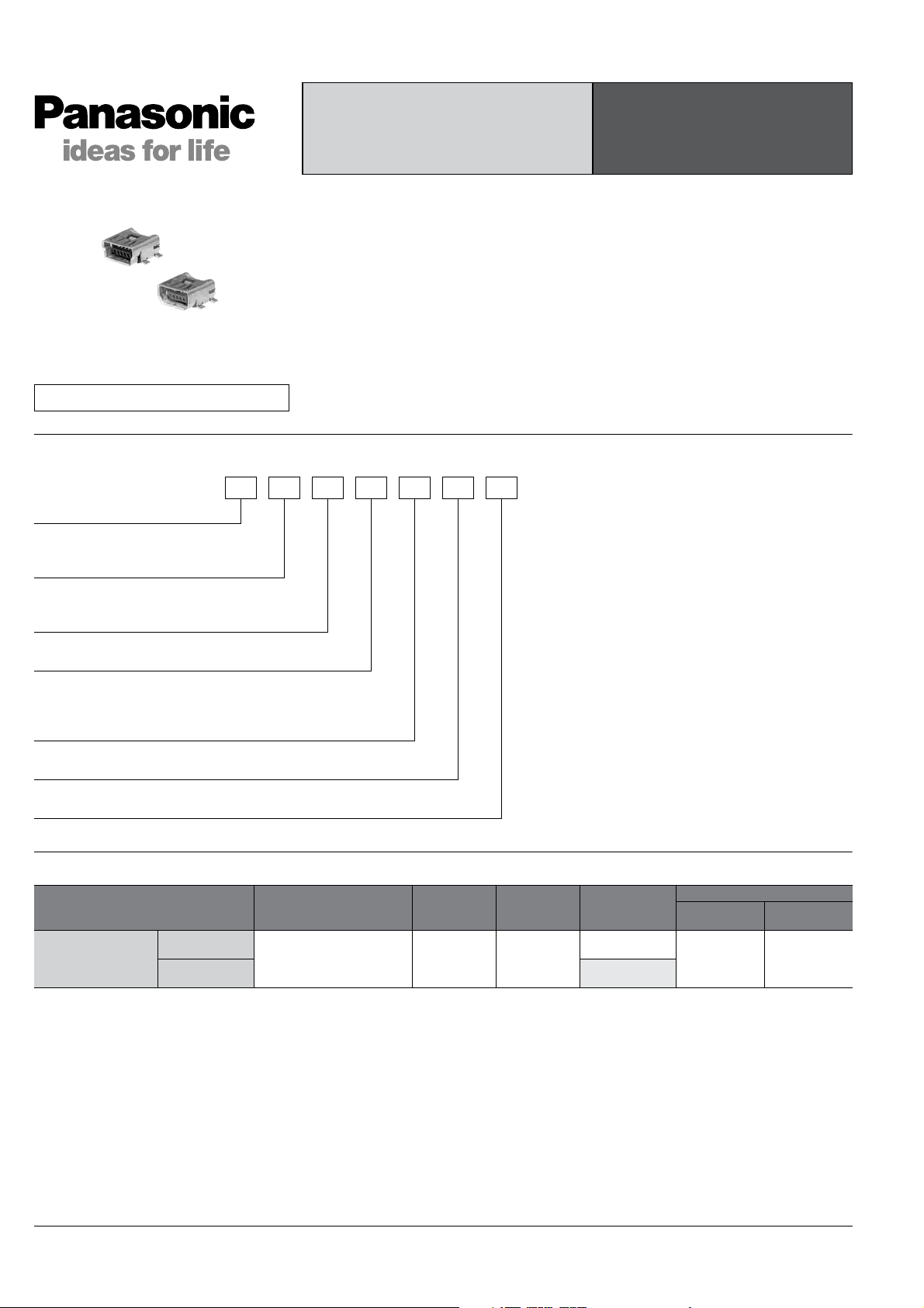
Mini USB (AXJ4)
CONNECTORS
APPLICATIONS
1. DSC, PMP, DVC, IC recorders
2. Mobile phones, PDA, smart phones
3. Compact PC peripherals (e.g.
external HDD, memory card readers)
4. Game machines
PRODUCT TYPES
Type Te r minal shape
5 contacts receptacle
(Compliant with the
Mini USB standard)
Mini B
Right angle type
Mini AB
Right angle type
Te r minal position: SMD
Clips (retention fitting): SMD
Positioning
bosses
Provided Without flange
Flange Part number
AXJ413110G
AXJ416110G
Packing quantity
Inner carton
(Embossed)
1,200 6,000
http://www.mew.co.jp/ac/e/Matsushita Electric Works, Ltd.
Outer carton
Page 2
SPECIFICATIONS
1. Characteristics
Item Specifications Conditions
Rated current 1.0A
Rated voltage 30V DC/AC
Contact resistance Max. 50mΩ
Electrical
characteristics
Mechanical
characteristics
Environmental
characteristics
Soldering
temperature
resistance
Insulation resistance Min. 100MΩ
Breakdown voltage
Electrostatic capacity Max. 2pF
Composite insertion
force (initial)
Composite removal
force (initial)
Ambient temperature –55°C to 85°C No freezing or condensation in low temperatures
Storage temperature –55°C to 85°C (–40°C to 50°C for packaging materials) No freezing or condensation in low temperatures
Vibration resistance
Impact resistance
Heat resistance
(mated)
Low temperature
resistance (mated)
Humidity resistance
(mated)
Temperature cycle test
(mated)
Saltwater spray
resistance (mated)
Hydrogen sulfide
Reflow soldering Peak temperature: Max. 260°C
Manual soldering
100V AC (Dielectric breakdown must not occur during a 1 min.
application)
Max. 35N
{3.57kgf}
Min. 7N {0.714kgf}
Discontinuity: Max. 1µs
Contact resistance: Max. 50mΩ
Appearance: No abnormality
Discontinuity: Max. 1µs
Contact resistance: Max. 50mΩ
Appearance: No abnormality
250 hours
Contact resistance: Max. 50mΩ
Withstand voltage: 100V AC dielectric breakdown must not
occur during a one-minute application.
Insulation resistance: Min. 100MΩ
Appearance: No abnormality
96 hours
Contact resistance: Max. 50mΩ
Withstand voltage: 100V AC dielectric breakdown must not
occur during a one-minute application.
Insulation resistance: Min. 100MΩ
Appearance: No abnormality
7 cycles
Contact resistance: Max. 50mΩ
Withstand voltage: 100V AC dielectric breakdown must not
occur during a one-minute application.
Insulation resistance: Min. 100MΩ
Appearance: No abnormality
10 cycles
Contact resistance: Max. 50mΩ
Withstand voltage: 100V AC dielectric breakdown must not
occur during a one-minute application.
Insulation resistance: Min. 100MΩ
Appearance: No abnormality
48 hours
Contact resistance: Max. 100mΩ
Appearance: No abnormality
96 hours
Contact resistance: Max. 100mΩ
Appearance: No abnormality
300±10°C: Max. 5 s
350±10°C: Max. 3 s
2. Material and surface treatment
Part name Material Surface treatment
Resin-molding portion Heat-resistant resin (UL94V-0) —
Metal parts
Pickup tape Heat-resistant resin —
Contact Copper alloy
Shell Copper alloy Ni plating on base, Sn plating on surface
Contact portion: Ni plating on base, Au plating on surface
Te r minal portion: Ni plating on base, Sn plating on surface
EIA-364-23
(Inductive resistance to wire is not included)
EIA-364-21
Using 100V DC megger
EIA-364-20
Detection current: 1mA
EIA-364-30
(Measure it between the adjacent terminals of the unmated
connector at a frequency of 1 kHz.)
EIA-364-13
Insert and remove a plug at a speed of 12.5 mm/min.
EIA-364-28
Apply vibration in three directions including the mating axis
that are perpendicular to one another for 15 minutes
respectively with a 100 mA DC current applied.
Cord length: 100mm Fix the cord end.
EIA-364-27
Acceleration: 294m/s
Duration: 11 ms,
Application directions: 6 surfaces (X, Y, and Z directions)
Number of applications: 3 times respectively (Total: 18 times)
Cord length: 100mm Fix the cord end.
EIA-364-17
Temperature: 85±2°C
Temperature: –55±2°C
EIA-364-31 Method III
Sequence
1. –55±3°C, 30 minutes
2. ~, Max. 5 minutes
3. 85±2°C, 30 minutes
4. ~, Max. 5 minutes
Bath temperature: 35±2°C
Saltwater concentration: 5±1%
Wash the connector with water at room temperature after the
test, and then dry it at room temperature.
Temperature :40±2°C
Humidity: 75 to 80%
Gas concentration: 3±1ppm
2
(30G)
AXJ4
Interface connectors
http://www.mew.co.jp/ac/e/Matsushita Electric Works, Ltd.
Page 3

AXJ4
DIMENSIONS
1. Mini B Right angle type
AXJ413110G
7.70
Terminal No.1
3.702.90
4×1.20
0.80
3.10
3.20
7.70
9.90
6.90
4.40
5.87
0.80±0.15
0.25
Terminal No.5
0.80 dia.
3.95
0.07
3.95
5.95
PC board edge
With a plug inserted:
Including the projection of the spring
4.40
in the shell contact section
mm General tolerance: ±0.3
Recommended PC board pattern
(TOP VIEW)
8.9±0.1
0.95±0.05 dia. (hole)
2.0±0.1
2.7±0.1
2.5±0.1
1.00±0.1
7.5±0.1
1.40±0.1
5.3±0.1
3.2±0.05
0.8±0.05
0.4±0.05
4.4±0.05
7.50±0.1
2. Mini AB Right angle type
mm General tolerance: ±0.3
AXJ416110G
Interface connectors
3.702.90
7.70
4×1.20
Terminal No.1
3.10
0.80
1.93
3.20
7.70
9.90
6.90
4.40
5.32
0.80±0.15
0.25
Terminal No.5
0.80 dia.
3.95
0.07
3.95
5.95
With a plug inserted:
Including the projection of the spring
4.40
in the shell contact section
Recommended PC board pattern
(TOP VIEW)
3.2±0.05
0.8±0.05
0.4±0.05
7.5±0.1
1.40±0.1
5.3±0.1
PC board edge
4.4±0.05
8.9±0.1
EMBOSSED TAPE DIMENSIONS (unit: mm)
• Tape dimensions (Conforming to JIS C 0806-3 1999) • Reel dimensions (Conforming to EIAJ ET-7200B)
24.0±0.3
11.5
1.75
4.0
2.0
380 dia.
25.4±1
Taping reel
Top cover tape
Embossed carrier tape
0.95±0.05 dia. (hole)
2.0±0.1
2.7±0.1
2.5±0.1
7.50±0.1
1.00±0.1
Pull out direction
12.0
1.5 dia.
Embossed mounting-hole
http://www.mew.co.jp/ac/e/Matsushita Electric Works, Ltd.
Page 4

NOTES
1. Use of a cover is recommended
when using this device in order to
prevent scraps, dust, dirt, etc., from
getting inside of the receptacle.
2. PC board design
Please refer to the recommended PC
board pattern to ensure the strength of
soldered portion of terminals.
3. Soldering
1) Manual soldering
• Please set up temperature and applied
time of soldering iron as indicated in
specification sheet.
• Please use soldering iron after
confirming removal of dispersed solder
flux on the contact surface by use of
magnifying glass after each soldering.
• Please properly clean soldeing iron.
2) Reflow soldering
• Screen printing is recommended for
cream solder printing.
• Screen thickness of 0.15mm is
recommended for cream solder printing.
• When applying different thickness of
screen, please consult us.
• Depending upon size of connector, self
alignments may not be expected.
Please pay attention to align terminals
and soldered pads.
• The following diagram shows the
recommended reflow soldering
temperature profile.
Temperature
Max. 260°C
150 to 175°C
• The temperature measured on the PC
board surface near connector terminals.
• After reflow soldering, in case of PC
board surface the reverse side using
reflow soldering, for example an adhesive
and so on connector of fixed disposition.
3) Rework of soldering portion
• Rework is one time.
• In case of soldering rework of bridges.
Please use a flat-head soldering iron and
don’t use supplementary solder flux.
• Please use the soldering iron under
specification’s temperature
Maximum temperature
Pre-heating
60 to 120 second
200°C
Max. 70 sec
Time
4. Since excessive force on the
terminals will cause deformation and
the integrity of the soldering will be
lost during reflow soldering, avoid
dropping or rough handling of the
product.
5. PC board warpage should be
controlled less than 0.03mm to entire
length of the connector.
6. Repeated bending of terminals and
holding parts can result in terminals
breaking.
7. Regarding after soldering
connectors on PC boards
• After mounting connectors on PC
boards, do not apply excessive loads to
the connector by piling up the boards.
• Please do not add the force to the
connector during assembled connector
on PC board.
8. This connector has metal shell for
preventing EMI, when designing an
enclosure the followings should be
considered. Guide for plug entrance
should be arranged in order to prevent
distorted insertions. Provide a cover
to reinforce the metal shell portions of
the receptacle.
9. We recommend the use of a
purified-water-based solution for
cleaning the PC board. If you use an
alcohol-based solution, the surface of
the molded part may be whitened. In
addition, please carefully monitor the
contamination degree of the solution
to prevent the solution from recontaminating the connector
contacts.
10. Others
To prevent insulation deterioration of PC
board after soldering, please avoid
adhesion coating agent to terminals in
case of coating.
For other details, please verify with
the product specification sheets.
AXJ4
Interface connectors
http://www.mew.co.jp/ac/e/Matsushita Electric Works, Ltd.
 Loading...