How it Works
Log In / Sign Up
Buy Points
How it Works
FAQ
Contact Us
Questions and Suggestions
Users
Panasonic
Loading...
A
AN8022L
AN8022SB
AN8025
AN8025M
AN8026
AN8027
AN8028
AN8029
AN8031
AN8032
AN8035
AN8035M
AN8037
AN8038
AN8038S
AN8041S
AN8045
AN8045M
AN8049FHN
AN8049SH
AN8060
AN8060S
AN8072N
AN8083S
AN8085
AN8085M
AN8086S
AN8090
AN8090S
AN80L18RMS
AN80L19RMS
AN80L20RMS
AN80L21RMS
AN80L22RMS
AN80L25RMS
AN80L28RMS
AN80L29RMS
AN80L30RMS
AN80L31RMS
AN80L32RMS
AN80L33RMS
AN80L34RMS
AN80L35RMS
AN80L36RMS
AN80L48RMS
AN80L49RMS
AN80L50RMS
AN80L51RMS
AN80L52RMS
AN80LXXRMS
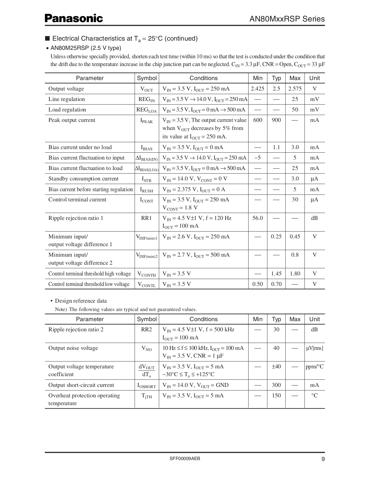
AN80MxxRSP
AN80PxxRSP
AN80xx
AN80xxM
AN8122K
AN8140K
AN8146FBQ
AN8221FB
AN8245K
AN8245SCR
AN8261
AN8267S
AN8353UB
AN8377N
AN8387S
AN8389S
AN8470NSA
AN8472SA
AN8473SA
AN8480NSB
AN8481SB
AN8488SB
AN8495SB
AN8497SA
AN8538SH
AN8539SH
AN8612NSB
AN8612NSR
AN8725FH
AN8730SB
AN8735NSB
AN8737SB
AN8746SA
AN8780SB
AN8783SB
AN8787NSB
AN8806SB
AN8807SB
AN8808SB
AN8813NSB
AN8814SB
AN8816SB
AN8819NFB
AN8837SB
AN8839NSB
AN8847SB
AN8849SB
AN8882SB
AN8946SB
AN90B00
Loading...
Loading...
Nothing found
AN80MxxRSP
Technical data
27 pgs
267.93 Kb
0
Table of contents
Loading...
Panasonic AN80MxxRSP Technical data
...
Panasonic Technical data
Download
Specifications and Main Features
Frequently Asked Questions
User Manual
Download
Loading...
+
18
hidden pages
Unhide
You need points to download manuals.
1 point = 1 manual.
You can buy points or you can get point for every manual you upload.
Buy points
Upload your manuals
 Loading...