

Panasonic AN8083S Datasheet
ICs for CD/CD-ROM Player
■ Overview
The AN8083S is an IC for controlling a DC-DC converter suitable for the switching power supply of various
portable equipments. It can operate with input voltage
1.1V or more.
■ Features
•
Operatable with low voltage input (PV
CC
>1.1V)
•
Decreased voltage detection circuit built-in
•
Short-circuit protection feature built-in
•
Provided with reset output
•
Synchronizable with outside clock
•
Low consumption current in stand-by mode
•
Output voltage in secondary side; 4.8V+0.3V (Variable
by using external resistance)
AN8083S
Low Voltage Operation IC for DC-DC Converter
0.1±0.1
1.5±0.2
0.3
0.65
0.15
0.4
1
2
3
4
5
6
7
8
16
15
14
13
12
11
10
9
0.4±0.25
1.27
Unit : mm
6.5
±0.3
4.2±0.3
10.1±0.3
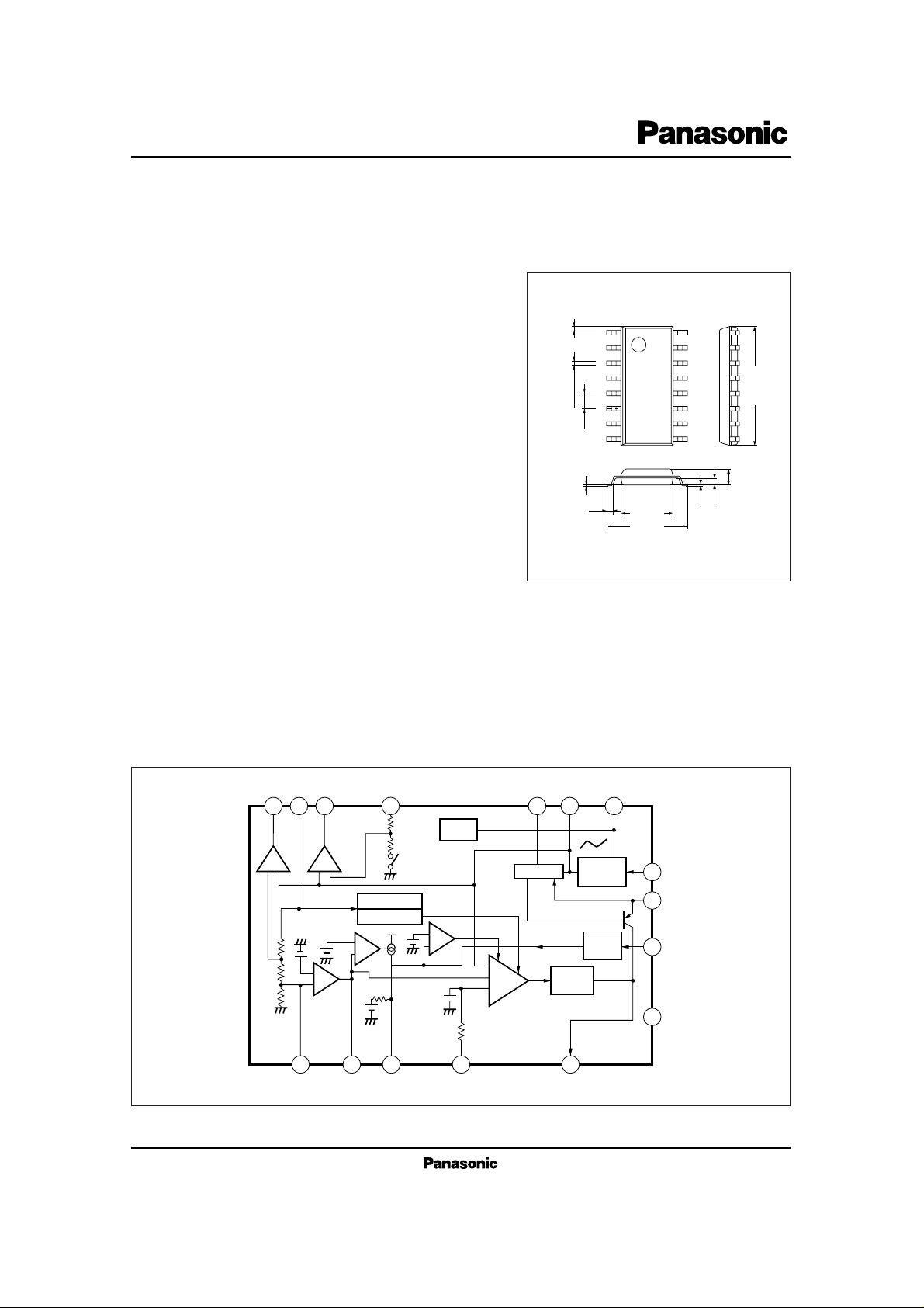
16-lead SOP package (SOP016-P-0225A)
15 1316 14 7
1 2 3 4 5
6
V
SEN
PV
CC
IN
10 12
9
8
11
Power
OFF
63kΩ
–+
GND
0.9V
1.25V
0.7V
4.2V
0.725V
30kΩ
2.0V
4.8V
1.25V 3.0 → 2.5V
2.15V
0.25V
0.85V
V
REF
–25µA
–+
–
+
+
–
+
–
+
–
+
RESET
EMP START
V
REF
CT
CLK
POWER
FB SPRO DED OUT
Starter SW
Early Value Set.
Starter
Switching
Circuit
Triangular
Wave
V
CC
■ Block Diagram
ICs for CD/CD-ROM Player
AN8083S
V
CC
PV
CC
P
D
T
opr
T
stg
Supply Voltage
Power Dissipation
Operating Ambient Temperature
Storage Temperature
V
mW
˚C
˚C
Parameter Symbol Rating Unit
■ Absolute Maximum Ratings (Ta=25˚C)
14.4
14.4
380
–20 ~ +75
–55 ~ +125
Paramenter Symbol Range
■ Recommended Operating Range (Ta=25˚C)
Operating Supply Voltage Range
V
CC
PV
CC
1.8V ~ 12V
1.1V ~ 12V
Parameter Symbol Condition min. typ. max. Unit
■ Electrical Characteristics (Ta=25˚C)
Power VCC Stand-by Mode Supply Current
I
PVCC
2 µA
V
CC
=0V, PVCC=3V
Power VCC Operating Mode Supply Current
I
PVCC
3 mA1.2
V
CC
=3.1V, PVCC=3V
Output Voltage
V
O
V4.8
Reset Output Threshold Voltage
4V
TH (RESET)
4.4 V
PV
CC
=3V
Decreased Voltage Detection Threshold Voltage
2.05V
TH (VSEN)
2.25 V2.15
PV
CC
=3V
Short-Circuit Protection Operating Voltage
1.35V
O (SPRO)
2.1 V
V
IN
=0V, V
POWER
=2V
Short-Circuit Protection Operating Voltage
1.7V
O (SPRO)
3.2 V
V
IN
=1V, V
POWER
=0V
Oscillation Frequency in Normal Operation
60f
OSC1
80 kHz70
R
REF
=33kΩ, CT=330pF
f
OSC2
80
100 120
kHzOscillation Frequency at Start
R
REF
=33kΩ, CT=330pF
V
CC
=1.9V, PVCC=3V
Output Voltage (Normal)
1.2V
OH (OUT)
1.6 V
I
O
= –20mA, VCT=0V
Output Voltage (Normal)
V
OL (OUT)
0.4 V
I
O
=20mA, VCT=1V
Note) Unless otherwise specified, V
CC
=4.8V, PVCC=3V
4.2
15 16 13 14 10 7 12
9
8
11
6
54321
+
2.15V
V
REF
4.8V
4.2V
0.7V
1.25V
2.0V
0.9V
30kΩ
–25µA
63kΩ
+
–
+
–
+
–
+
–
+
+ –
3.0V→ 2.5V
33kΩ
0.01µF
IN FB
SPRO
47µF
DED
0.01µF
OUT
GND
0.01µF
100Ω
POWER
CLK
PV
CC
4.8V±0.3V
33kΩ330pF
V
REF
CT
START
V
SENSE
EMP
V
CC
+ –
Power
OFF
0.25V
0.85V
1.25V
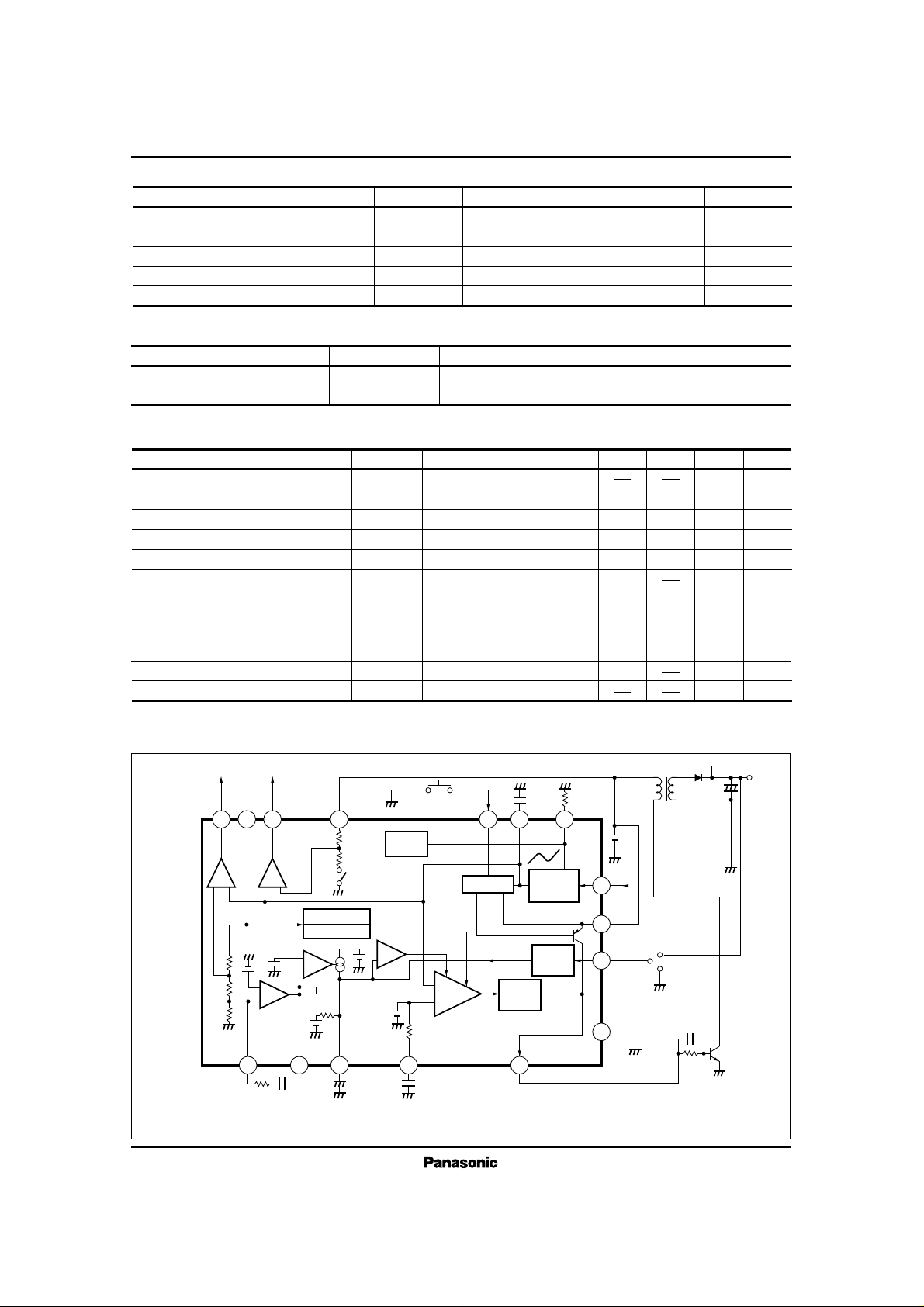
Connect Pin11 to the secondary side and Pin10 to GND at oscillation start. (Pin10 is always open.)
RESET
0.725V
Starter SW
Initial set
Starter
SW
circuit
+
Triangular
Wave
■ Application Circuit
 Loading...