

Panasonic AN8049SH Datasheet
Voltage Regulators
AN8049SH
1.8-volt 3-channel step-up, step-down, and polarity inverting
DC-DC converter control IC
■ Overview
The AN8049SH is a three-channel PWM DC-DC
converter control IC that features low-voltage operation.
This IC can form a power supply that provides two stepup outputs and one step-down or polarity inverted output
with a minimal number of external components. The
AN8049SH features the ability to operate from a supply
voltage as low as 1.8 V, and thus can be operated from
two dry-batteries.
6.5±0.3
24 13
+0.10
5.5±0.3
7.5±0.3
(0.50)
112
0.65±0.100.65±0.10
1.5±0.20.1±0.1
– 0.05
0.15
Unit : mm
0° to 10°
■ Features
(0.50)
0.50
Seating plane
0.2±0.1
• Wide operating supply voltage range: 1.8 V to 14 V
• High-precision reference voltage circuit
—V
REF
pin voltage: ±1%
SSOP024-P-0300A
— Error amplifier: ±1.5%
• Surface mounting package for miniaturized and thinner power supplies
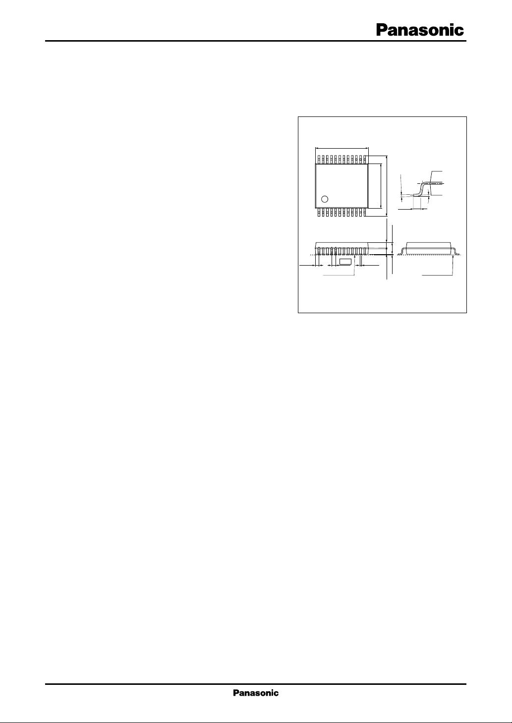
Package: SSOP-24D
0.5-mm lead pitch
7.8 mm × 6.8 mm × t 1.9 mm
• Supports control over a wide output frequency range: 20 kHz to 1 MHz
• On/off (sequence control) pins provided for each channel for easy sequence control setup
• The negative supply error amplifier supports 0-volt input.
Common-mode input voltage range: − 0.1 V to V
−1.4 V
CC
This allows the number of external components to be reduced by two resistors.
• Fixed duty factor: 86%
However, the duty can be adjusted to anywhere from 0% to 100% with an external resistor.
• Timer latch short-circuit protection circuit (charge current: 1.1 µA typical)
• Low input voltage malfunction prevention circuit (U.V.L.O.) (operation start voltage: 1.67 V typical)
• Standby function (active-high control input, standby mode current: 1 µA maximum)
• Alternate package versions also available.
Part No.: AN8049FHN
Package: QFN-24
0.5-mm lead pitch
5.4 mm × 4.4 mm × t 0.8 mm
Seating plane
■ Applications
• Electronic equipment that requires a power supply system
1
AN8049SH Voltage Regulators
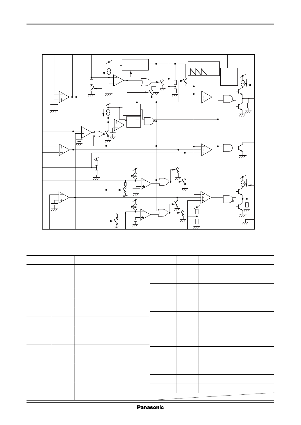
■ Block Diagram
S.C.P.
FB3
IN+3
IN−3
DT3
CTL3
IN-123FB124CTL1
Error
amplifier 1
1.26 V
1
20
Error
amplifier 2
18
S.C.P. comp.
19
2
5
Error
amplifier 3
1.26 V
21
22
V
7
1.1 µA
0.9 V
REF
20 kΩ
V
CC
1.1 µA
44 kΩ56 kΩ
20 kΩ
CC
V
16
Reference voltage
supply
1.26 V
U.V.L.O.
1.26 V
1.1 µA
1.1 µA
20 kΩ
6
V
REF
(Allowance: ±1%)
R
Q
S
Latch
1.26 V
1.26 V
REF
V
9
1.26 V
4
DT1
45 kΩ
55 kΩ
3
OSC
17
Sawtooth wave generator
0.7 V
0.3 V
PWM1
PWM3
PWM2
V
REF
45 kΩ
55 kΩ
Off
8
On/off
control
V
CC
V
CC
11
RB1
12
OUT1
27 kΩ
15
OUT3
10
RB2
13
OUT2
27 kΩ
14
GND
IN−2
FB2
■ Pin Descriptions
Pin No. Symbol Description
1 S.C.P. Connection for the capacitor
2 DT3 Channel 3 soft start setting
3 DT2 Channel 2 soft start setting
4 DT1 Channel 1 soft start setting
5 CTL3 Channel 3 on/off control
6 CTL2 Channel 2 on/off control
7 CTL1 Channel 1 on/off control
8 Off On/off control
9V
10 RB2 Connection for the OUT2
11 RB1 Connection for the OUT1
2
that provides the shortcircuit protection circuit time
constant
Reference voltage output
REF
block output source current
setting resistor
block output source current
setting resistor
CTL2
DT2
Pin No. Symbol Description
12 OUT1 OUT1 block push-pull output
13 OUT2 OUT2 block push-pull output
14 GND Ground
15 OUT3 OUT3 block open-collector output
16 V
CC
Supply voltage
17 OSC Oscillator circuit timing resistor and
capacitor connection
18 IN+3 Error amplifier 3 noninverting input
19 IN−3 Error amplifier 3 inverting input
20 FB3 Error amplifier 3 output
21 IN−2 Error amplifier 2 inverting input
22 FB2 Error amplifier 2 output
23 IN−1 Error amplifier 1 inverting input
24 FB1 Error amplifier 1 output
Voltage Regulators AN8049SH
■ Absolute Maximum Ratings
Parameter Symbol Rating Unit
Supply voltage V
Off pin allowable application V
CC
OFF
voltage
CTL pin allowable application V
CTL
voltage
Error amplifier input pin V
allowable application voltage
*
Supply current I
OUT1 and OUT2 pin output I
2
IN
CC
SO(OUT)
source current
OUT3 pin output current I
1
Power dissipation
*
Operating temperature T
Storage temperature T
Note) 1. Do not apply external currents or voltages to any pins not specifically mentioned. For circuit currents, '+' denotes current
flowing into the IC, and '−' denotes current flowing out of the IC.
2. Items other than the storage temperature, operating temperature, and power dissipation are all stipulated for an ambient
temperature Ta = 25°C.
3.*1: Ta = 85°C. See the "Application Notes" for details on the relationship between IC power dissipation and the ambient
temperature.
2: When VCC < 6 V, the following condition must hold: V
*
O
P
D
opr
stg
14.2 V
14.2 V
VCC − 0.2 V
6V
mA
−50 mA
+50 mA
146 mW
−30 to +85 °C
−55 to +125 °C
= V
IN−1
= VCC − 0.2 V.
IN−2
■ Recommended Operating Range
Parameter Symbol Range Unit
Off pin application voltage V
OUT1 and OUT2 pin output source current I
OUT3 pin output current I
Timing resistance R
Timing capacitance C
Oscillator frequency f
Short-circuit protection time-constant setting capacitance C
Output current setting resistance R
OFF
SO(OUT)
O
T
T
OUT
SCP
B
0 to 14 V
−40 to −1mA
40 (max.)
3 to 33 kΩ
100 to 10 000 pF
20 to 1 000 kHz
1 000 (min.) pF
750 to 15 000 Ω
3
AN8049SH Voltage Regulators
■ Electrical Characteristics at V
= 2.4 V, C
CC
Parameter Symbol Conditions Min Typ Max Unit
Reference voltage block
Reference voltage V
Line regulation with input fluctuation
REFIREF
Line V
Load regulation Load I
U.V.L.O. block
Circuit operation start voltage V
UON
Error amplifier 1 block
Input threshold voltage 1 V
Input bias current 1 I
High-level output voltage 1 V
Low-level output voltage 1 V
Output source current 1 I
Output sink current 1 I
TH1
B1
EH1
EL1
SO(FB)1
SI(FB)1
Error amplifier 2 block
Input threshold voltage 2 V
Input bias current 2 I
High-level output voltage 2 V
Low-level output voltage 2 V
Output source current 2 I
Output sink current 2 I
TH2
B2
EH2
EL2
SO(FB)2
SI(FB)2
Error amplifier 3 block
Input offset voltage V
Common-mode input voltage range V
Input bias current 3 I
High-level output voltage 3 V
Low-level output voltage 3 V
Output source current 3 I
Output sink current 3 I
IO
ICR
B3
EH3
EL3
SO(FB)3
SI(FB)3
Oscillator block
Oscillator frequency f
OUT
= 0.1 µF, Ta = 25°C
REF
= − 0.1 mA 1.247 1.26 1.273 V
= 1.8 V to 14 V 220mV
CC
= − 0.1 mA to −1 mA −20 −3 mV
REF
1.59 1.67 1.75 V
1.241 1.26 1.279 V
0.1 0.2 µA
1.0 1.2 1.4 V
0.2 V
−38 −31 −24 µA
0.5 mA
1.241 1.26 1.279 V
0.1 0.2 µA
1.0 1.2 1.4 V
0.2 V
−38 −31 −24 µA
0.5 mA
−6 6mV
− 0.1 V
CC
V
−1.4
− 0.6 − 0.3 µA
1.0 1.2 1.4 V
0.2 V
−38 −31 −24 µA
0.5 mA
RT = 7.5 kΩ, CT = 680 pF 170 190 210 kHz
4
Voltage Regulators AN8049SH
■ Electrical Characteristics at V
Parameter Symbol Conditions Min Typ Max Unit
Output 1 block
Output duty factor 1 Du
High-level output voltage 1 V
Low-level output voltage 1 V
Output source current 1 I
Output sink current 3 I
Pull-down resistor 1 R
Output 2 block
Output duty factor 2 Du
High-level output voltage 2 V
Low-level output voltage 2 V
Output source current 2 I
Output sink current 2 I
Pull-down resistor 2 R
Output 3 block
Output duty factor 3 Du
Output saturation voltage V
Output leakage current I
Short-circuit protection circuit block
Input standby voltage V
Input threshold voltage V
Input latch voltage V
Charge current I
On/off control block
Input threshold voltage V
CTL block
Input threshold voltage V
Charge current I
Whole Device
Average consumption current I
Standby mode current I
= 2.4 V, C
CC
RT = 7.5 kΩ, CT = 680 pF 80 86 92 %
1
OH1IO
OL1IO
SO(OUT)1VO
SI(OUT)1VO
O1
RT = 7.5 kΩ, CT = 680 pF 80 86 92 %
2
OH2IO
OL2IO
SO(OUT)2VO
SI(OUT)2VO
O2
RT = 7.5 kΩ, CT = 680 pF 80 86 92 %
3
O(SAT)IO
V13 = 14 V 1 µA
OLE
STBY
THPC
IN
V
CHG
ON(TH)
THCTL
V
CTL
CC(OFF)RB
CC(SB)
= 0.1 µF, Ta = 25°C (continued)
REF
= −10 mA, RB = 1 kΩ VCC −1 V
= 10 mA, RB = 1 kΩ0.2 V
= 0.7 V, RB = 1 kΩ−34 −29 −24 mA
= 0.7 V, RB = 1 kΩ 40 mA
17 27 37 kΩ
= −10 mA, RB = 1 kΩ VCC −1 V
= 10 mA, RB = 1 kΩ0.2 V
= 0.7 V, RB = 1 kΩ−34 −29 −24 mA
= 0.7 V, RB = 1 kΩ 40 mA
17 27 37 kΩ
= 40 mA 0.5 V
0.1 V
0.8 0.9 1.0 V
0.1 V
= 0 V −1.43 −1.1 − 0.77 µA
SCP
0.6 0.9 1.2 V
1.07 1.26 1.45 V
= 0 V −1.43 −1.1 − 0.77 µA
CTL
= 9.1 kΩ, duty = 50% 4.2 5.5 mA
1 µA
5
AN8049SH Voltage Regulators
■ Electrical Characteristics at Ta = 25°C (continued)
•
Design reference data
Note: The characteristics listed below are reference values related to the IC design and are not guaranteed.
Parameter Symbol Conditions Min Typ Max Unit
Reference voltage block
V
temperature characteristics V
REF
RFEdTTa
Error amplifier 1 block
VTH temperature characteristics V
Open loop gain 1 A
THdT1Ta
V1
Error amplifier 2 block
VTH temperature variation V
Open loop gain 2 A
THdT2
V2
Error amplifier 3 block
Open loop gain 3 A
V3
Oscillator block
Frequency supply voltage f
DV
characteristics RT = 7.5 kΩ, CT = 680 pF
Frequency temperature f
DT
characteristics RT = 7.5 kΩ, CT = 680 pF
Short-circuit protection circuit block
Comparator threshold voltage V
THL
On/off control block
Off pin current I
OFF
= −30°C to +85°C 1 %
= −30°C to +85°C 1.5 %
80 dB
1.5 %
80 dB
80 dB
VCC = 1.8 V to 14 V 1 %
Ta = −30°C to +85°C 3 %
1.26 V
V
= 5 V 38 µA
OFF
6
Voltage Regulators AN8049SH
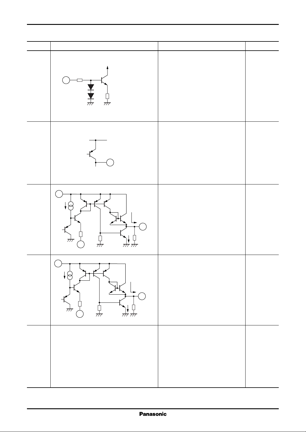
■ Terminal Equivalent Circuits
Pin No. Equivalent circuit Description I/O
1 S.C.P.: O
2 DT3: I
3 DT2: I
4 DT1: I
V
CC
1.5 kΩ
2
4
3
1.1 µA
1
44 kΩ
46 kΩ
45 kΩ
55 kΩ
45 kΩ
55 kΩ
1.26 V
9
9
9
Latch
S
R
20 17
22 17
24 17
Q
Output
shutoff
PWM3
PWM2
PWM1
Connection for the capacitor that sets
the timer latch short-circuit protection
circuit time constant. Use a capacitor
with a value of 1 000 pF or higher.
The charge current I
is 1.1 µA
CHG
typical.
Sets the channel 3 soft start time.
Set the time by connecting a capacitor
between this pin and ground.
(See the "Application Notes, [7]" section.)
Note that although the channel 3
maximum on duty is set internally to
86%, the maximum on duty can be
adjusted by connecting resistors between
this pin and ground, and between this
pin and the V
pin. (See the "Application
REF
Notes, [6]" section.)
Sets the channel 2 soft start time.
Set the time by connecting a capacitor
between this pin and ground.
(See the "Application Notes, [7]" section.)
Note that although the channel 2
maximum on duty is set internally to
86%, the maximum on duty can be
adjusted by connecting resistors
between this pin and ground, and
between this pin and the V
REF
pin.
(See the "Application Notes, [6]" section.)
Sets the channel 1 soft start time.
Set the time by connecting a capacitor
between this pin and ground.
(See the "Application Notes, [7]" section.)
Note that although the channel 1
maximum on duty is set internally to
86%, the maximum on duty can be
adjusted by connecting resistors
between this pin and ground, and
between this pin and the V
REF
pin.
(See the "Application Notes, [6]" section.)
7
AN8049SH Voltage Regulators
■ Terminal Equivalent Circuits (continued)
Pin No. Equivalent circuit Description I/O
5 CTL3: I
Controls the on/off state of channel 3. A
delay can be provided in the power supply
V
CC
20 kΩ
1.1 µA
High
Channel 3
1.26 V
output operation
5
6 CTL2: I
V
CC
20 kΩ
1.1 µA
High
Channel 2
1.26 V
output operation
6
7 CTL1: I
V
CC
20 kΩ
1.1 µA
High
Channel 1
1.26 V
output operation
7
turn-on start time by connecting a capacitor
between this pin and ground.
(See the "Application Notes, [9]" section.)
t
= 1.26 (V) × C
DLY3
(µF)/1.1 (µA) (s)
CTL3
This pin can also be used to control the
on/off state with an external signal. In that
case, the allowable input voltage range is
from 0 V to V
. Note that during
CC
U.V.L.O. and timer latch operation, this
pin is connected to ground through a
20 kΩ resistor.
Controls the on/off state of channel 2.
A delay can be provided in the power
supply turn-on start time by connecting
a capacitor between this pin and
ground.
(See the "Application Notes, [9]" section.)
t
= 1.26 (V) × C
DLY2
(µF)/1.1 (µA) (s)
CTL2
This pin can also be used to control the
on/off state with an external signal.
In that case, the allowable input voltage
range is from 0 V to V
. Note that
CC
during U.V.L.O. and timer latch operation,
this pin is connected to ground through a
20 kΩ resistor.
Controls the on/off state of channel 1.
A delay can be provided in the power
supply turn-on start time by connecting
a capacitor between this pin and
ground. (See the "Application Notes, [9]"
section.)
t
= 1.26 (V) × C
DLY1
(µF)/1.1 (µA) (s)
CTL1
This pin can also be used to control the
on/off state with an external signal.
In that case, the allowable input voltage
range is from 0 V to V
. Note that
CC
during U.V.L.O. and timer latch operation,
this pin is connected to ground through a
20 kΩ resistor.
8
Voltage Regulators AN8049SH
■ Terminal Equivalent Circuits (continued)
Pin No. Equivalent circuit Description I/O
8 Off: I
Start and stop of
internal circuits.
8
100 kΩ
9V
V
CC
9
10 RB2: I
16
I
SO(OUT)2
13
10
200 Ω
I
SI(OUT)2
30 kΩ
Controls the on/off state.
When the input is high: normal
operation
(V
> 1.2 V)
OFF
When the input is low: standby mode
(V
< 0.6 V)
OFF
In standby mode, the total current
consumption is held to under 1 µA.
:O
REF
Outputs the internal reference voltage.
The reference voltage is 1.26 V
(allowance: ±1%) when V
2.4 V and I
is − 0.1 mA. Insert a
REF
CC
is
capacitor of at least 0.1 µF between
V
and ground for phase
REF
compensation.
Connection for a resistor that sets the
channel 2 output current.
Use a resistor in the range 750 Ω to
15 kΩ.
11 RB1: I
16
Connection for a resistor that sets the
channel 1 output current.
I
SO(OUT)1
Use a resistor in the range 750 Ω to
15 kΩ.
12
11
200 Ω
I
SI(OUT)1
30 kΩ
12 See pin 11. OUT1: O
Push-pull output.
The absolute maximum rating for the
output source current is −50 mA.
The output source current is set by the
external resistor connected to the RB1
pin.
9
 Loading...