

Voltage Regulators
AN8049FHN
1.8-volt 3-channel step-up, step-down, and polarity inverting
DC-DC converter control IC
■ Overview
The AN8049FHN is a three-channel PWM DC-DC
converter control IC that features low-voltage operation.
This IC can form a power supply that provides two stepup outputs and one step-down or polarity inverted output
with a minimal number of external components. Minimal
operating supply voltage of this IC is as low as 1.8 V, so
that it can operate from 2 dry-batteries.
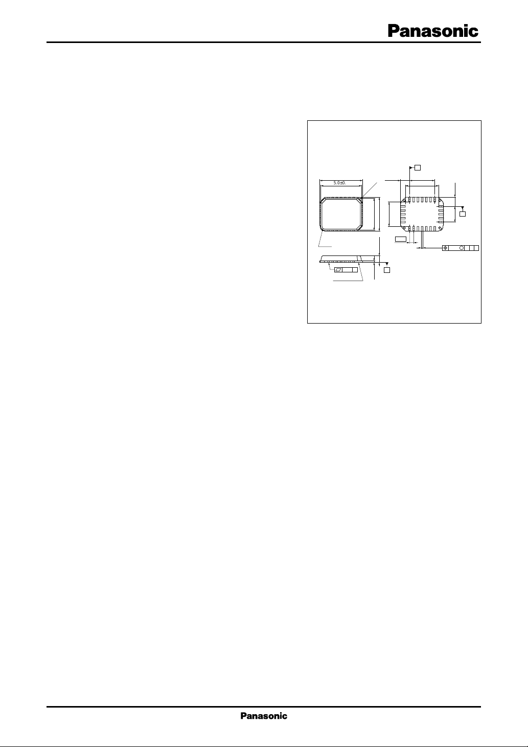
And also, it is housed in an ultrathin, 4-directional-
5.2±0.2 (1.10) 3.0±0.2
5.0±0.1
19 13
20
24
1
R0.3
3-C0.5
12
8
lead SMD-package whose thickness is 0.8 mm maximum
and pin-pitch is 0.5 mm therefore it is most suitable for
making a power supply small and thin.
0.10
Seating plane
■ Features
• Wide operating supply voltage range: 1.8 V to 14 V
• High-precision reference voltage circuit
— V
pin voltage: ±1%
REF
— Error amplifier: ±1.5%
• Ultrathin surface mounting package for miniaturized and thinner power supplies
Package: QFN-24
0.5-mm lead pitch
5.4 mm × 4.4 mm × t 0.8 mm
• Supports control over a wide output frequency range: 20 kHz to 1 MHz
• On/off (sequence control) pins provided for each channel for easy sequence control setup
• The negative supply error amplifier supports 0-volt input.
Common-mode input voltage range: − 0.1 V to V
−1.4 V
CC
This allows the number of external components to be reduced by two resistors.
• Fixed duty factor: 86%
However, the duty can be adjusted to anywhere from 0% to 100% with an external resistor.
• Timer latch short-circuit protection circuit (charge current: 1.1 µA typical)
• Low input voltage malfunction prevention circuit (U.V.L.O.)
(operation start voltage: 1.67 V typical)
• Standby function (active-high control input, standby mode current: 1 µA maximum)
QFN024-P-0405
4.0±0.1
4.2±0.2
0.80max.
0.2±0.1
3.0±0.1
S
A
4.0±0.1
13
12
8
7
0.50
Unit: mm
19
17
0.2±0.1
20
2.0±0.2 (1.10)
24
0.10 SSA B
B
M
■ Applications
• Electronic equipment that requires a power supply system
1
AN8049FHN Voltage Regulators
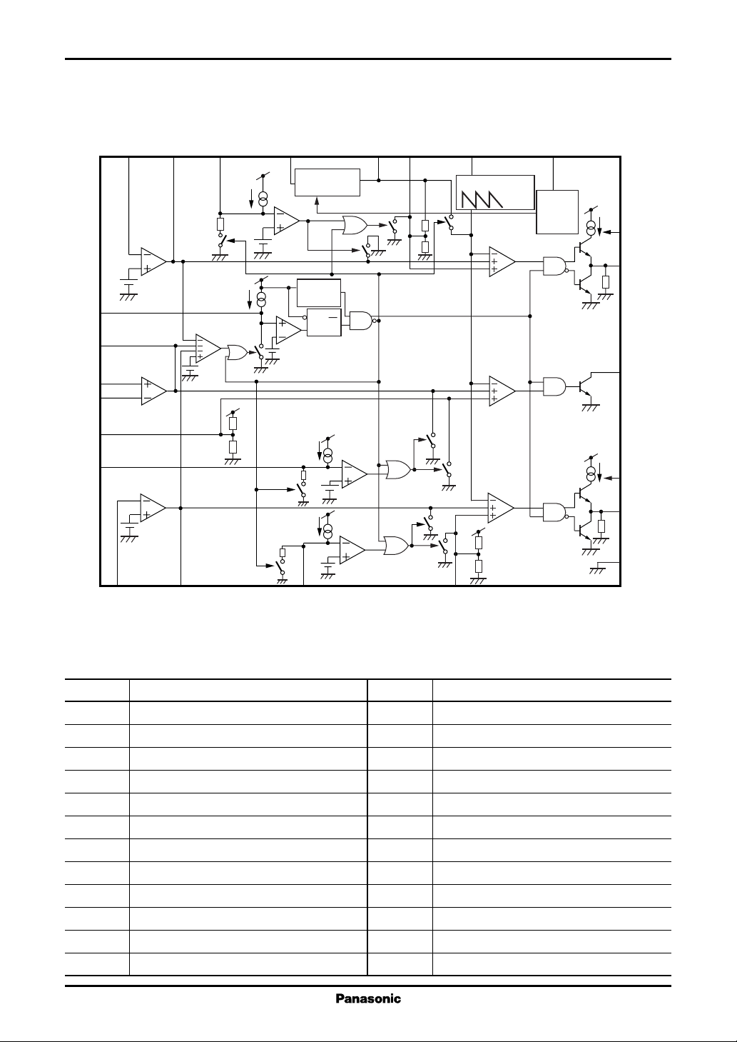
■ Block Diagram
S.C.P.
FB3
IN+3
IN−3
DT3
CTL3
IN-121FB122CTL1
Error
amplifier 1
1.26 V
23
18
S.C.P. comp.
Error
amplifier 2
16
17
24
3
Error
amplifier 3
1.26 V
19
20
V
REF
5
1.1 mA
0.9 V
1.1 mA
20 kΩ
V
CC
50 kΩ50 kΩ
20 kΩ
CC
V
14
Reference voltage
supply
1.26 V
U.V.L.O.
1.26 V
1.1 mA
1.1 mA
20 kΩ
4
7
V
REF
1.26 V
(Allowance: ±1%)
R
Q
S
Latch
1.26 V
1.26 V
REF
V
2
DT1
50 kΩ
OSC
15
Triangular wave generator
50 kΩ
PWM1
PWM3
PWM2
1
0.7 V
0.3 V
V
REF
50 kΩ
50 kΩ
Off
6
On/off
control
V
CC
V
CC
9
RB1
10
OUT1
30 kΩ
13
OUT3
8
RB2
11
OUT2
30 kΩ
12
GND
IN−2
FB2
■ Pin Descriptions
Pin No. Description
1 DT2
2 DT1
3 CTL3
4 CTL2
5 CTL1
6 Off
7V
8 RB2
9 RB1
10 OUT1
11 OUT2
12 GND
2
REF
CTL2
DT2
Pin No. Description
13 OUT3
14 V
CC
15 OSC
16 IN+3
17 IN−3
18 FB3
19 IN−2
20 FB2
21 IN−1
22 FB1
23 S.C.P.
24 DT3
Voltage Regulators AN8049FHN
■ Absolute Maximum Ratings
Parameter Symbol Rating Unit
Supply voltage V
Off pin allowable application voltage V
Error amplifier input allowable V
application voltage
*2
OUT1 and OUT2 pin output I
CC
OFF
IN
SO(OUT)
source current
OUT3 pin output current I
Power dissipation
*1
Operating temperature T
Storage temperature T
Note)*1: Ta = 85°C. For the independent IC without a heat sink.
2: When VCC is less than 6 V, V
*
IN−1
SI(OUT)
and V
P
D
opr
stg
must be VCC.
IN+2
14.2 V
14.2 V
V
CC
V
−50 mA
+50 mA
111 mW
−30 to +85 °C
−55 to +150 °C
■ Recommended Operating Range
Parameter Symbol Range Unit
Off pin application voltage V
OUT1 and OUT2 pin output source current I
OUT3 pin output current I
Timing resistance R
Timing capacitance C
Oscillator frequency f
Short-circuit protection time-constant setting capacitance C
Output current setting resistance R
OFF
SO(OUT)
SI(OUT)
T
T
OUT
SCP
B
0 to 14 V
−40 (min.) mA
40 (max.) mA
3 to 33 kW
100 to 1 000 pF
20 to 1 000 kHz
1 000 (min.) pF
750 to 15 000 Ω
3
AN8049FHN Voltage Regulators
■ Electrical Characteristics at V
= 2.4 V, C
CC
Parameter Symbol Conditions Min Typ Max Unit
Reference voltage block
Reference voltage V
REFIREF
Line regulation with input fluctuation Line V
Load regulation Load I
V
temperature characteristics V
REF
V
pin short-circuit current I
REF
RFEdTTa
OC
U.V.L.O. block
Circuit operation start voltage V
UON
Error amplifier 1 block
Input threshold voltage 1 V
Input bias current 1 I
High-level output voltage 1 V
Low-level output voltage 1 V
Output source current 1 I
Output sink current 1 I
VTH temperature characteristics 1 V
Open-loop gain 1 A
TH1
B1
EH1
EL1
SO(FB)1
SI(FB)1
THdT1Ta
V1
Error amplifier 2 block
Input threshold voltage 2 V
Input bias current 2 I
High-level output voltage 2 V
Low-level output voltage 2 V
Output source current 2 I
Output sink current 2 I
VTH temperature characteristics 2 V
Open-loop gain 2 A
TH2
B2
EH2
EL2
SO(FB)2
SI(FB)2
THdT2Ta
V2
Error amplifier 3 block
Input offset voltage V
Common-mode input voltage range V
Input bias current 3 I
High-level output voltag 3 V
Low-level output voltage 3 V
Output source current 3 I
Output sink current 3 I
Open-loop gain 3 A
IO
ICR
B3
EH3
EL3
SO(FB)3
SI(FB)3
V3
= 0.1 µF, Ta = 25°C
REF
= − 0.1 mA 1.247 1.26 1.273 V
= 1.8 V to 14 V 220mV
CC
= −0.1 mA to −1 mA −20 −3 mV
REF
= −30°C to +85°C 1 %
−10 mA
1.59 1.67 1.75 V
1.241 1.26 1.279 V
0.1 0.2 µA
1.0 1.2 1.4 V
0.2
−38 −31 −24 µA
0.5 mA
= −30°C to +85°C 1.5 %
80 dB
1.241 1.26 1.279 V
0.1 0.2 µA
1.0 1.2 1.4 V
0.2
−38 −31 −24 µA
0.5 mA
= −30°C to +85°C 1.5 %
80 dB
−6 6mV
− 0.1 V
CC
−1.4
− 0.6 − 0.3 µA
1.0 1.2 1.4 V
0.2
−38 −31 −24 µA
0.5 mA
80 dB
V
4
Voltage Regulators AN8049FHN
■ Electrical Characteristics (continued) at V
= 2.4 V, C
CC
= 0.1 µF, Ta = 25°C
REF
Parameter Symbol Conditions Min Typ Max Unit
Oscillator block
Oscillator frequency f
Frequency supply voltage f
RT = 7.5 kΩ, CT = 680 pF 170 190 210 kHz
OUT
RT = 7.5 kΩ, CT = 680 pF 1 %
DV
characteristics
Frequency temperature f
RT = 7.5 kΩ, CT = 680 pF 3 %
DT
characteristics
Output 1 block
Output duty factor 1 Du1RT = 7.5 kΩ, CT = 680 pF 80 86 92 %
High-level output voltage 1 V
Low-level output voltage 1 V
Output source current 1 I
Output sink current 1 I
SO(OUT)1VO
SI(OUT)1VO
Pull-down resistor 1 R
OH1IO
OL1IO
O1
= −10 mA, RB = 1 kΩ VCC −1 V
= 10 mA, RB = 1 kΩ0.2 V
= 0.7 V, RB = 1 kΩ−32 −27 −22 mA
= 0.7 V, RB = 1 kΩ 40 mA
20 30 40 kΩ
Output 2 block
Output duty factor 2 Du2RT = 7.5 kΩ, CT = 680 pF 80 86 92 %
High-level output voltage 2 V
Low-level output voltage 2 V
Output source current 2 I
Output sink current 2 I
SO(OUT)2VO
SI(OUT)2VO
Pull-down resistor 2 R
OH2IO
OL2IO
O2
= −10 mA, RB = 1 kΩ VCC −1 V
= 10 mA, RB = 1 kΩ0.2 V
= 0.7 V, RB = 1 kΩ−32 −27 −22 mA
= 0.7 V, RB = 1 kΩ 40 mA
20 30 40 kΩ
Output 3 block
Output duty factor 3 Du3RT = 7.5 kΩ, CT = 680 pF 80 86 92 %
Output saturation voltage V
O(SAT)
0.2 V
Short-circuit protection circuit block
Input standby voltage V
Input threshold voltage V
Input latch voltage V
Charge current I
Comparator threshold voltage V
STBY
THPC
IN
CHG
THL
V
= 0 V −1.3 −1.0 −0.7 µA
SCP
0.1 V
0.8 0.9 1.0 V
0.1 V
1.26 V
On/off control block
Input threshold voltage V
Off pin current I
ON(TH)
OFF
V
= 5 V 35 µA
OFF
0.7 1.0 1.3 V
CTL block
Input threshold voltage V
Charge current I
THCTL
CTL
V
= 0 V −1.3 −1.0 −0.7 µA
CTL
1.07 1.26 1.47 V
Whole device
Average consumption current I
Standby mode current I
CC(OFF)RB
CC(SB)
= 9.1 kΩ, duty = 50% 4.2 5.5 mA
1 µA
5
AN8049FHN Voltage Regulators
■ Terminal Equivalent Circuit
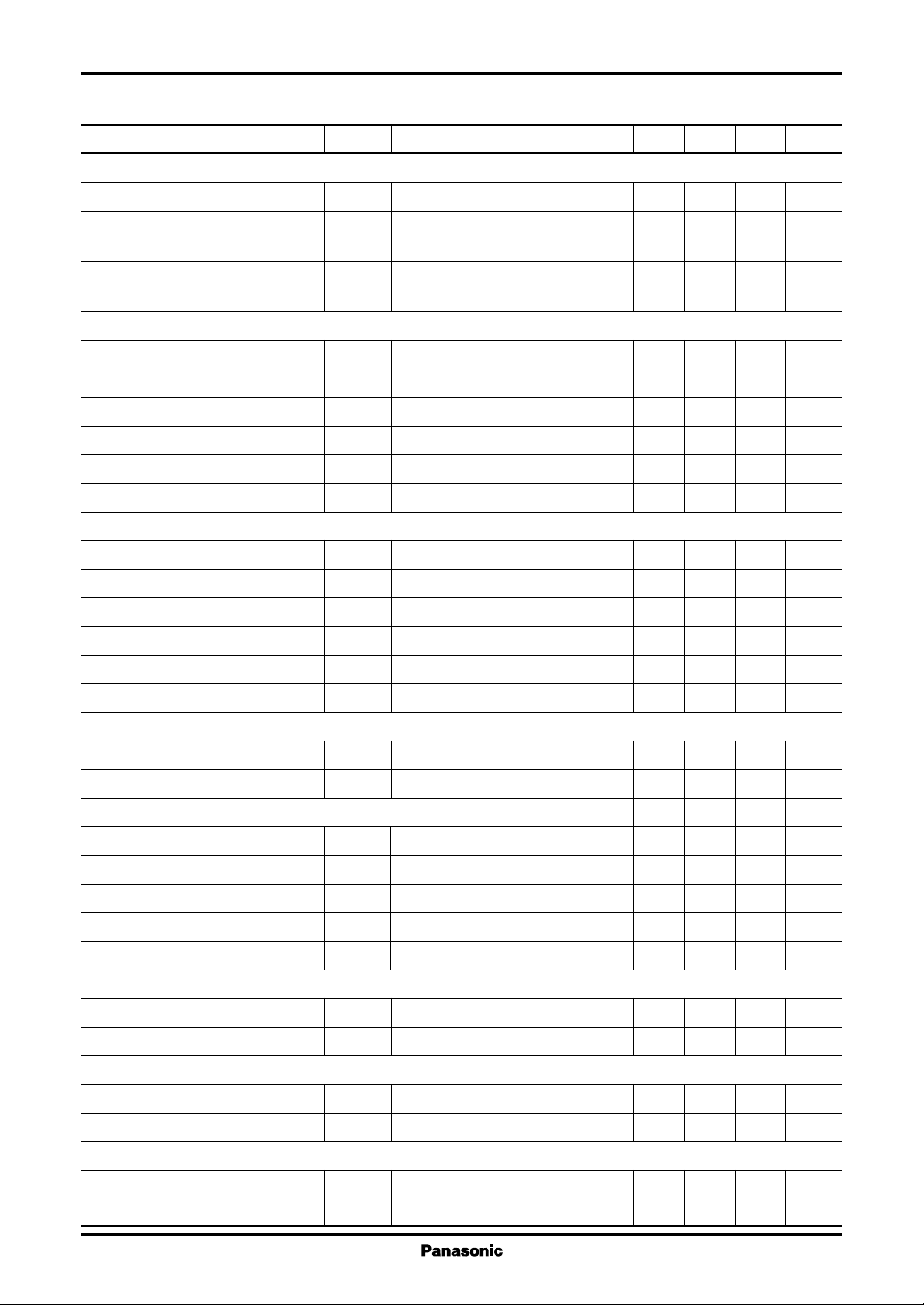
Pin No. Equivalent circuit Description I/O
1 DT2: I
Sets the channel 2 soft start time.
Set the time by connecting a capacitor
7 1520
50 kΩ
1
50 kΩ
PWM2
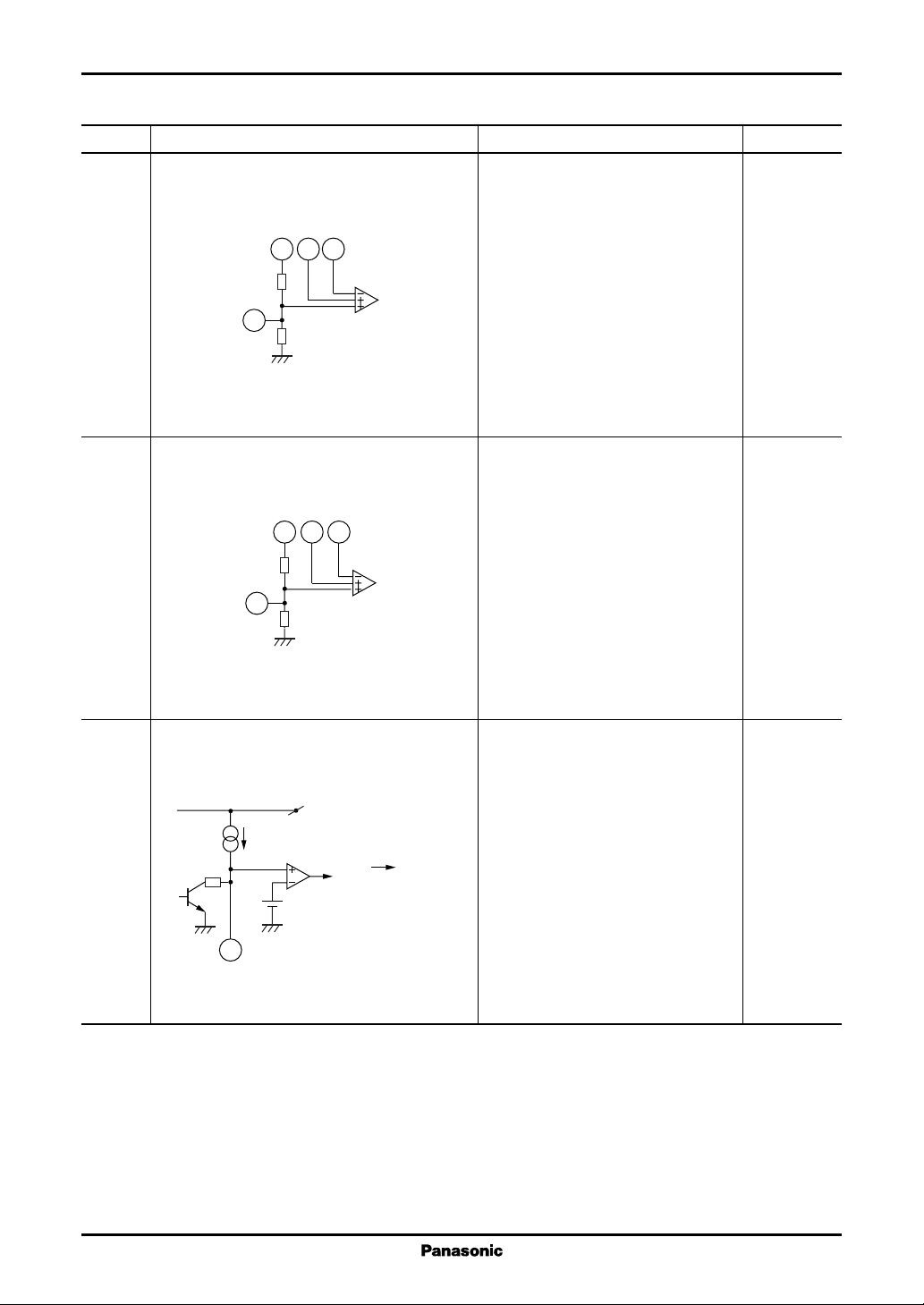
2 DT1:
227
15
50 kΩ
2
50 kΩ
PWM1
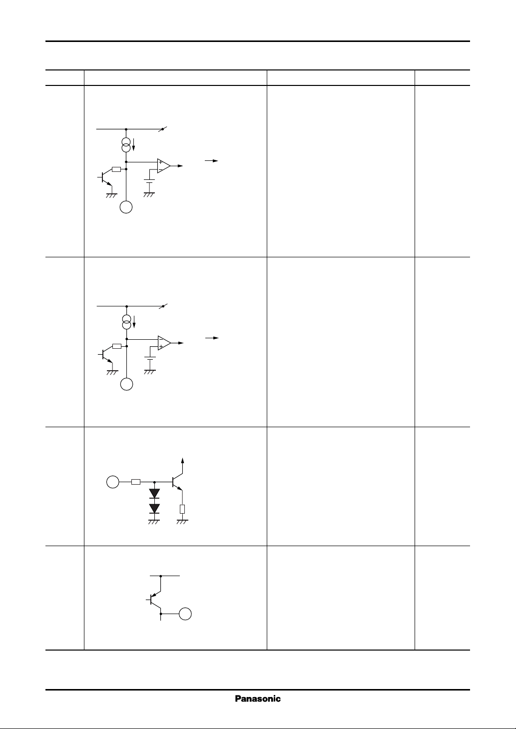
3 CTL3: I
V
CC
20 kΩ
1.1 µA
High
channel 3 operation
1.26 V
is turned off.
3
between this pin and ground.
Note that although the channel 2
maximum on duty is set internally to
86%, the maximum on duty can be set
to a value of 86% or less by inserting
a resistor between this pin and ground,
and can be set to a value of 86% or
more by inserting a resistor between
this pin and the V
REF
pin.
Sets the channel 1 soft start time.
Set the time by connecting a capacitor
between this pin and ground.
Note that although the channel 1
maximum on duty is set internally to
86%, the maximum on duty can be set
to a value of 86% or less by inserting
a resistor between this pin and ground,
and can be set to a value of 86% or
more by inserting a resistor between
this pin and the V
REF
pin.
Controls the on/off state of channel 3.
A delay can be provided in the power
supply turn-on start time by connecting
a capacitor between this pin and ground.
t
= 1.26 (V) × C
DLY3
(µF)/1.1 (µA) (s)
CTL3
This pin can also be used to control the
on/off state with an external signal.
In that case, the allowable input voltage
range is from 0 V to V
. Note that
CC
during U.V.L.O. and timer latch
operation, this pin is connected to
ground through a 20 kΩ resistor.
6
Voltage Regulators AN8049FHN
■ Terminal Equivalent Circuit (continued)
Pin No. Equivalent circuit Description I/O
4 CTL2: I
Controls the on/off state of channel 2.
V
CC
20 kΩ
1.1 µA
High
channel 2 operation
1.26 V
is turned off.
4
5 CTL1: I
V
CC
20 kΩ
1.1 µA
High
channel 1 operation
1.26 V
is turned off.
5
6 Off: I
Start and stop of
internal circuits.
6
100 kΩ
7V
V
CC
7
A delay can be provided in the power
supply turn-on start time by connecting
a capacitor between this pin and ground.
t
= 1.26 (V) × C
DLY2
(µF)/1.1 (µA) (s)
CTL2
This pin can also be used to control the
on/off state with an external signal.
In that case, the allowable input voltage
range is from 0 V to V
. Note that
CC
during U.V.L.O. and timer latch
operation, this pin is connected to
ground through a 20 kΩ resistor.
Controls the on/off state of channel 1.
A delay can be provided in the power
supply turn-on start time by connecting
a capacitor between this pin and ground.
t
= 1.26 (V) × C
DLY1
(µF)/1.1 (µA) (s)
CTL1
This pin can also be used to control the
on/off state with an external signal.
In that case, the allowable input voltage
range is from 0 V to V
. Note that
CC
during U.V.L.O. and timer latch
operation, this pin is connected to
ground through a 20 kΩ resistor.
Controls the on/off state.
When the input is high: normal
operation
(V
> 1.2 V)
OFF
When the input is low: standby mode
V
< 0.6 V)
OFF
In standby mode, the total current
consumption is held to under 1 µA.
:O
REF
Outputs the internal reference voltage.
The reference voltage is 1.26 V
(allowance: ±1%) when V
and I
is −0.1 mA. Insert a capacitor
REF
of at least 0.1 µF between V
is 2.4 V
CC
REF
and
ground for phase compensation.
7
 Loading...