

Voltage Regulators
AN8041S
Liquid crystal backlight control IC
■ Overview
The AN8041S is an inverter control IC for liquid
crystal backlight using PWM method. The output
voltage of DC-DC converter and the current of cathode-ray tube can be controlled by using two error
amplifiers, so that the system is designed easily.
Since the n-channel MOSFET can be directly
driven, it is possible to construct a highly effective
power supply.
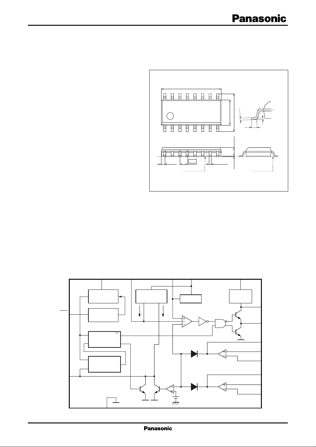
16 9
18
10.1±0.3
4.2±0.3
6.5±0.3
■ Features
• Operating supply voltage: 3.6 V to 34 V
• Totem pole output circuit: Output current of ±500 mA
• Built-in bootstrap circuit
• N-channel power MOSFET can be directly driven
• Built-in two error amplifier circuits allow both the
voltage and current control
• Incorporating on/off functions (active-high control input, standby mode current is 5 µA or less)
• Built-in timer latch short-circuit protection circuit
• Maximum oscillation frequency: 500 kHz
Note)*: The voltage is limited to the range of 3.6 V to 17 V if used in a step-down circuit.
*
(0.605)
1.27
Seating plane
0.40±0.25
0.1±0.1 1.5±0.2
SOP016-P-0225A
■ Applications
• LCD displays, digital still cameras, and PDAs
(0.15)
0.3
Unit: mm
(0° to 10°)
Seating plane
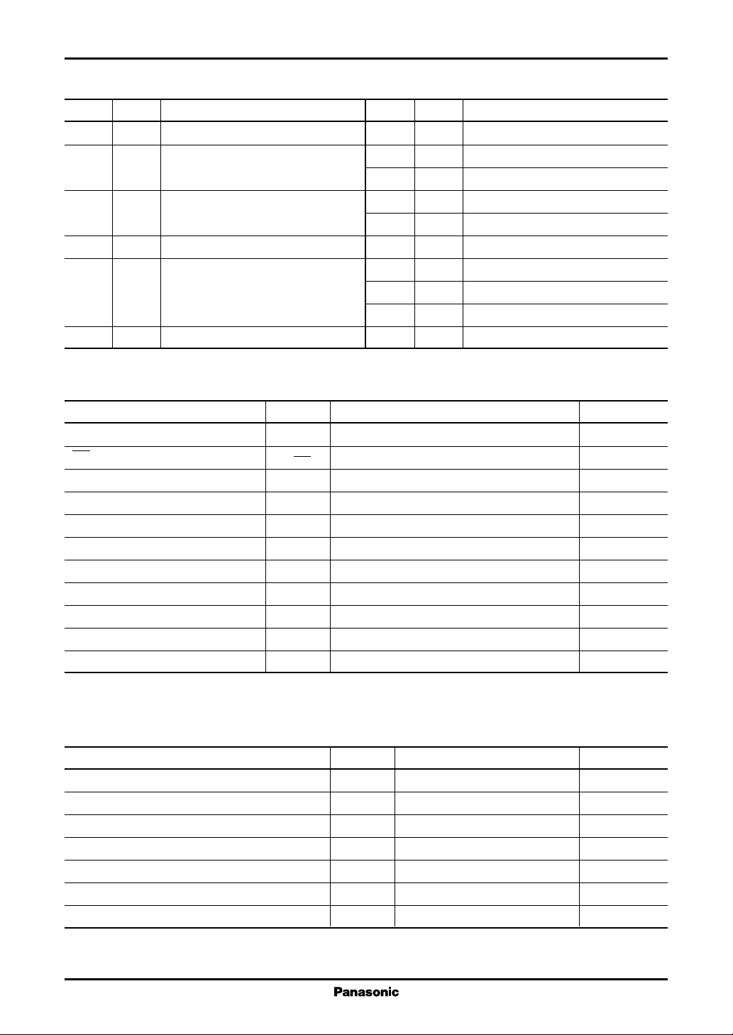
■ Block Diagram
Off
S.C.P.
16
5
REF
V
1
V
REF
2.57 V
On/off
active-high
R
U.V.L.O.
S
R
Latch
S
12
Q
Q
Q
GND
DTC
4
Constant
current source
S.C.P.
comp.
CT
3
PWM comp.
2
OSC
RT
Error amp. 1
Error amp. 2
CC
V
15
Bootstrap
14
13
11
10
CB
Out
8
FB1
6
IN+1
7
IN−1
9
FB2
IN+2
IN−2
1
AN8041S Voltage Regulators
■ Pin Descriptions
Pin No. Symbol Description
1V
Reference voltage output pin
REF
2 RT Pin for connecting oscillator
timing resistor
3 CT Pin for connecting oscillator
timing capacitor
4 DTC Dead-time control pin
5 S.C.P. Pin for connecting the time constant
setting capacitor for short-circuit
protection
6IN+1
Error amplifier 1 noninverted input pin
■ Absolute Maximum Ratings
Parameter Symbol Rating Unit
Supply voltage V
Off terminal application voltage V
Error amplifier input voltage V
DTC terminal application voltage V
Out terminal application voltage V
CB terminal application voltage V
Out terminal constant output current I
Out terminal peak output current I
Power dissipation
Operating ambient temperature
Storage temperature
Note)*: Expect for the operating ambient temperature and storage temperature, all ratings are for Ta = 25°C.
*
*
*
CC
OFF
I
DTC
OUT
CB
O
O(PEAK)
P
D
T
opr
T
stg
Pin No. Symbol Description
7IN−1 Error amplifier 1 inverted input pin
8 FB1 Error amplifier 1 output pin
9 FB2 Error amplifier 2 output pin
10 IN−2 Error amplifier 2 inverted input pin
11 IN+2
Error amplifier 2 noninverted input pin
12 GND Grounding pin
13 Out Output pin
14 CB Bootstrap output circuit
15 V
Power supply voltage application pin
CC
16 Off On/off control pin
35 V
35 V
− 0.3 to V
− 0.3 to V
REF
REF
35 V
35 V
±100 mA
±500 mA
143 mW
−30 to +85 °C
−40 to +125 °C
V
V
■ Recommended Operating Range
Parameter Symbol Range Unit
Supply voltage (when using step-down circuit) V
Supply voltage (when using step-up circuit) V
Oscillation frequency f
Oscillator timing resistance R
Oscillator timing capacitance C
Error amplifier input voltage V
Reference voltage output current I
2
CC
CC
OUT
IN
REF
3.6 to 17 V
3.6 to 34 V
5 to 500 kHz
T
T
5.1 to 30 kΩ
100 to 10 000 pF
− 0.1 to +0.8 V
−1 to 0 mA
Voltage Regulators AN8041S
■ Electrical Characteristics at VCC = 12 V, RT = 15 kΩ, CT = 120 pF, Ta = 25°C
Parameter Symbol Conditions Min Typ Max Unit
Reference voltage block
Output voltage V
REFIREF
Input regulation with input fluctuation Line VCC = 3.6 V to 34 V 725mV
Load regulation Load I
Output voltage V
TC1Ta
temperature characteristics 1
Output voltage V
TC2Ta
temperature characteristics 2
Output short-circuit current I
OS
U.V.L.O. block
Circuit operation start voltage V
Hysteresis width V
UON
HYS
Error amplifier block
Input offset voltage V
Input bias current I
Common-mode input voltage range V
High-level output voltage 1 V
Low-level output voltage 1 V
Output sink current I
Output source current I
Open-loop gain A
IO
B
ICR
EH
EL
SINK
SOURCEVFB
G
Dead-time control circuit block
Input current I
Low-level input threshold voltage V
High-level input threshold voltage V
DTC
DT-L
DT-H
Output block
Oscillation frequency f
OUT
Output duty ratio Du R
Low-level output voltage V
High-level output voltage V
Frequency f
OLIO
OHIO
dV
supply voltage characteristics VCC = 3.6 V to 34 V
Frequency f
dT1fOUT
temperature characteristics 1 Ta = −30°C to +25°C
Frequency f
dT2fOUT
temperature characteristics 2 Ta = 25°C to 85°C
= −1 mA 2.483 2.57 2.647 V
= − 0.1 mA to −1 mA 110mV
REF
= −30°C to +25°C ±1 %
= 25°C to 85°C ±1 %
−10 mA
2.8 3.1 3.4 V
60 140 220 mV
−6 6mV
−500 −25 nA
− 0.1 0.8 V
V
REF
− 0.3 V
REF
− 0.1
V
0.1 0.3 V
VFB = 0.9 V 8 mA
= 0.9 V −110 µA
70 dB
RT = 15 kΩ−14.8 −12.3 −9.8 µA
Duty = 0% 0.45 0.65 V
Duty = 100% 1.2 1.4 V
RT = 15 kΩ, 180 200 220 kHz
CT = 120 pF
= 75 kΩ 45 50 55 %
DTC
= 70 mA 1.0 1.3 V
= −70 mA VCB−2.0 VCB−1.0 V
f
= 200 kHz, ±3 V
OUT
= 200 kHz, ±9 V
= 200 kHz, ±9 V
3
AN8041S Voltage Regulators
■ Electrical Characteristics at VCC = 12 V, RT = 15 kΩ, CT = 120 pF, Ta = 25°C (continued)
Parameter Symbol Conditions Min Typ Max Unit
Bootstrap circuit block
Input standby voltage V
Oscillator block
RT terminal voltage V
Short-circuit protection block
Input threshold voltage V
Input standby voltage V
Input latch voltage V
Charge current I
Comparator threshold voltage V
On/off control block
Threshold voltage V
Whole device
Total consumption current I
Standby current I
CC(SB)
INCBICB
RT
THPC
STBY
IN
CHG
THL
TH
CC
= −70 mA
VCC−1.2 VCC−1.0 VCC− 0.8
0.37 V
0.70 0.75 0.80 V
30 120 mV
30 120 mV
−2.76 −2.3 −1.84 µA
1.82 V
0.8 2.0 V
3.9 5.0 mA
5 µA
V
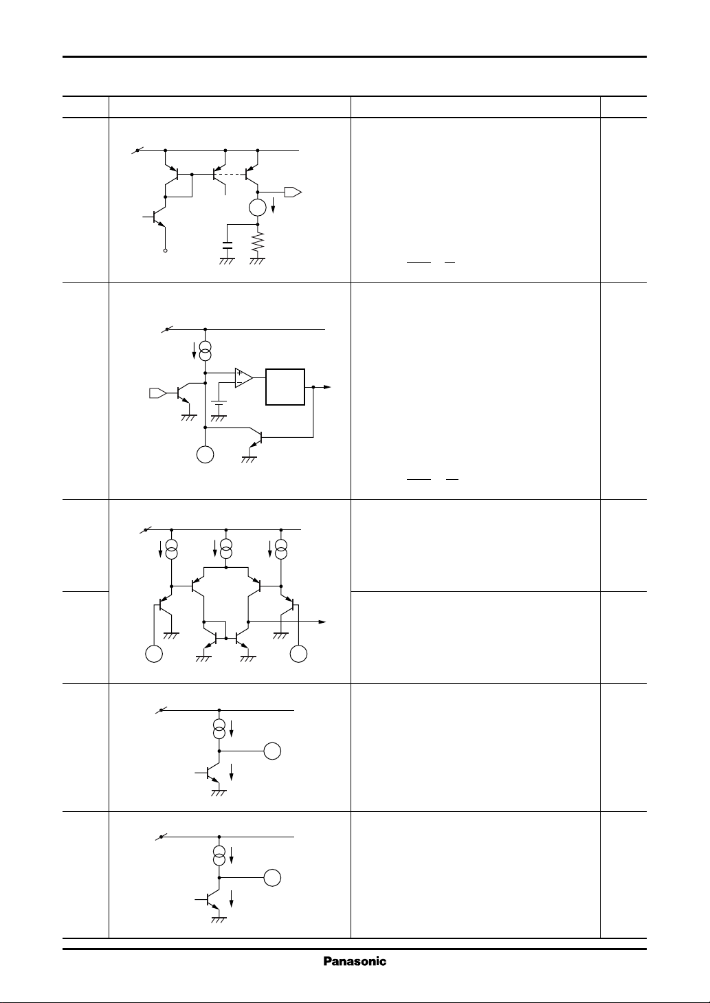
■ Terminal Equivalent Circuits
Pin No. Equivalent circuit Description I/O
1V
V
CC
1
2 RT:
3 CT:
V
REF
V
REF
To PWM input
OSC
comp.
100 Ω
2
RT (≈ 0.37 V)
DTC S.C.P.
I
O
3
2I
O
:O
REF
The reference voltage output terminal
(2.57 V (allowance: ±3%)).
Incorporating short-circuit protection against
GND.
The terminal used for connecting a timing resistor to set oscillator's frequency.
Use a resistance value within the range of 5.1 kΩ
to 30 kΩ.
The terminal voltage is approx. 0.37 V.
The terminal used for connecting a timing capacitor to set oscillator's frequency.
Use a capacitance value within the range of 100
pF to 10 000 pF.
For frequency setting method, refer to the
" Application Notes, [3] Function descriptions "
section. Use an oscillation frequency in the range
of 5 kHz to 500 kHz.
4
Voltage Regulators AN8041S
■ Terminal Equivalent Circuits (continued)
Pin No. Equivalent circuit Description I/O
4 DTC:
5 S.C.P.:
6IN+1: I
7IN−1: I
8 FB1: O
9 FB2: O
V
REF
RT
V
REF
I
CHG
To U.V.L.O.
V
REF
V
REF
V
REF
The terminal for connecting a resistor and ca-
PWM
comparator
input
I
4
DTC
C
DTC
R
DTC
pacitor to set the dead-time and soft start period
of PWM output. Input current I
is determined
DTC
by the timing resistor RT , so that dispersion and
fluctuation with temperature are suppressed. It
is approx. −12.3 µA when R
V
=
RT
×1[A]
RT2
I
DTC
= 15 kΩ.
T
The terminal for connecting a capacitor to set the
time constant of soft start and timer latch shortcircuit protection circuit.
0.75 V
Latch
S
R
Q
Use a capacitance value in the range of more than
1 000 pF.
The charge current I
is determined by the
CHG
timing resistor RT , so that dispersion and fluctuation with temperature are suppressed. It is
5
approx. −1.3 µA when R
V
=
RT
×1[A]
RT11
I
CHG
= 15 kΩ.
T
The noninverted input terminal of the error amplifier 1.
For common-mode input, use in the range of
− 0.1 V to +0.8 V.
The inverted input terminal of the error amplifier 1.
67
For common-mode input, use in the range of
− 0.1 V to +0.8 V.
The output terminal of the error amplifier 1.
Source current
8
Sink current
Source current: approx. −120 µA
Sink current : approx. 8 mA
Correct the frequency characteristics of the gain
and the phase by connecting a resistor and a capacitor between this terminal and IN−1 terminal.
The output terminal of the error amplifier 2.
Source current
9
Sink current
Source current: approx. −120 µA
Sink current : approx. 8 mA
Correct the frequency characteristics of the gain
and the phase by connecting a resistor and a capacitor between this terminal and IN−2 terminal.
5
 Loading...