

Panasonic AN8038S, AN8038 Datasheet
Voltage Regulators
AN8038, AN8038S
AC-DC switching power supply control IC
with RCC local resonance circuit for
improved conformance with
energy conservation laws
■ Overview
The AN8038 and AN8038S are self-excited AC-DC
switching power supply control IC that adopt RCC local
resonance control. These ICs are designed to achieve high
efficiency over a wide range of loads (light loads at the
standby mode to heavy loads) for improved conformance
with energy conservation laws, and support input levels
used worldwide. They are particularly appropriate for use
in AV and OA equipments.
■ Features
• Supports improved conformance with energy conser-
vation laws by providing two operating modes.
With external resistors, it is possible to set the operating
point at which the modes change over according to the
load power, as shown below.
1.Continuous (RCC) mode
High efficiency achieved with local resonance operation (zero cross detection).
2.Discontinuous mode (standby) mode
Reduced switching loss and standby power due to reduced frequency
• Input voltage correction function. This function corrects
the maximum on-period in a manner inversely proportional to the input voltage.
• Built-in overvoltage protection function (detects at V
• Pulse-by-pulse overcurrent protection function (single detection per one cycle)
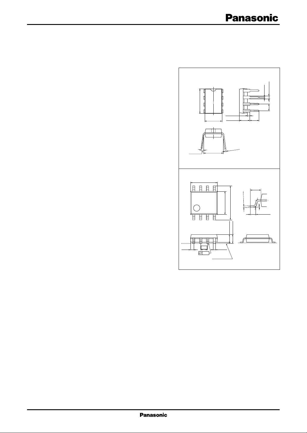
• Packages: 8-pin DIP ··· AN8038
8-pin SOP··· AN8038S
CC
pin)
AN8038 Unit: mm
3° to 15°
AN8038S Unit: mm
(0.60)
1
2
3
9.4±0.3
4
6.3±0.3
7.62±0.25
DIP008-P-0300B
5.01±0.20
1.27
0.10
Seating plane
SOP008-P-0225C
8
7
6
5
0.51 min.
3.8±0.25
.1
0
+
5
.0
0
–
0.15
58
0.15±0.10
6.40±0.20
4.30±0.20
41
1.75 max.
1.45±0.10
+0.10
0.40
–0.05
(3.45)
(1.05)
0.5±0.1
0° to10°
0.50±0.20
1.2±0.25
2.54
■ Applications
• Facsimiles and other OA equipment
• Printers and other personal computer peripheral equipment
• AV equipment
1
AN8038, AN8038S Voltage Regulators
■ Block Diagram
CC
V
8
RSTB
IFB
TR
2
4
High-side
1
Low-side
OVP
17.5
kΩ
17.5
kΩ
I/V
conv .
clamp
clamp
7 V
4.2 V
OVP
S
V
FB
Current
reviser (ITR)
0.25 V
(SD latch)
RQ
S
(TR latch)
INIT
R
Q
Current
reviser (IFB)
1.0 V
Start
Stop
3
V
REF
7 V
Q
In
In
Q
Out
7
Out
6
GND
drive
Q
Q
Q
CF
latch
Q
T
ON
S
T
OFF
R
R
5
CLM
− 0.2 V
CF
2
Voltage Regulators AN8038, AN8038S
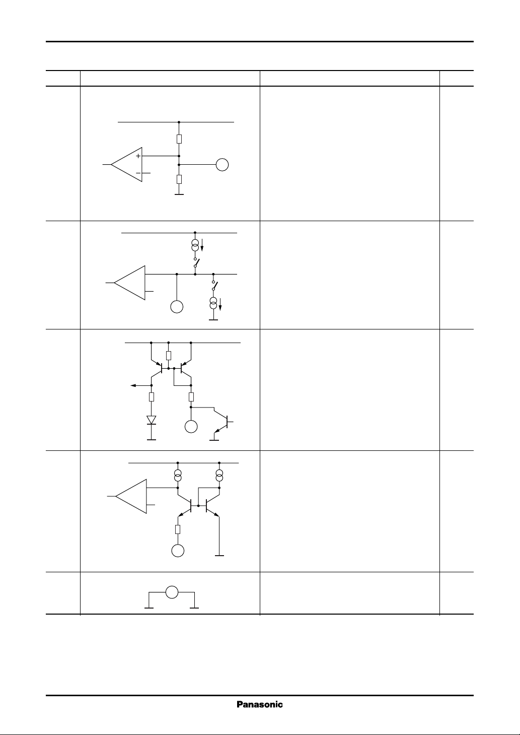
■ Pin Descriptions
Pin No. Symbol Description
1 TR Transformer reset. When a transformer reset is detected, i.e., a low level is input to this pin, the IC
output goes high.
However, the transformer reset signal is ignored during the minimum off-period determined by
the CF pin. The maximum on-period is also corrected according to the current flowing out of this
pin.
2 RSTB Adjusts the light-load detection level that determines the when the IC switches from RCC to
discontinuous operation. When the voltage (V
signal from IFB pin goes up higher than this pin, minimum off-period current at CF pin decreases,
and operating frequency decreases.
The detection level can be adjusted arbitrarily using an external pull-down resistor.
3 CF Connection for the capacitor that determines the on and off periods for the IC output (Out).
4 IFB Input for the current feedback signal from the power supply output photocoupler
5 CLM Input of the pulse-by-pulse overcurrent protection circuit. Normally, it will be necessary to add
an external filter for this input.
6 GND Ground
7V
8V
Output to drive a power MOSFET directly
OUT
Power supply. This pin watches VCC , and has operating threshold voltages for the start, stop,
CC
OVP, and OVP reset levels.
) which is I-V conversion of current feedback
FB
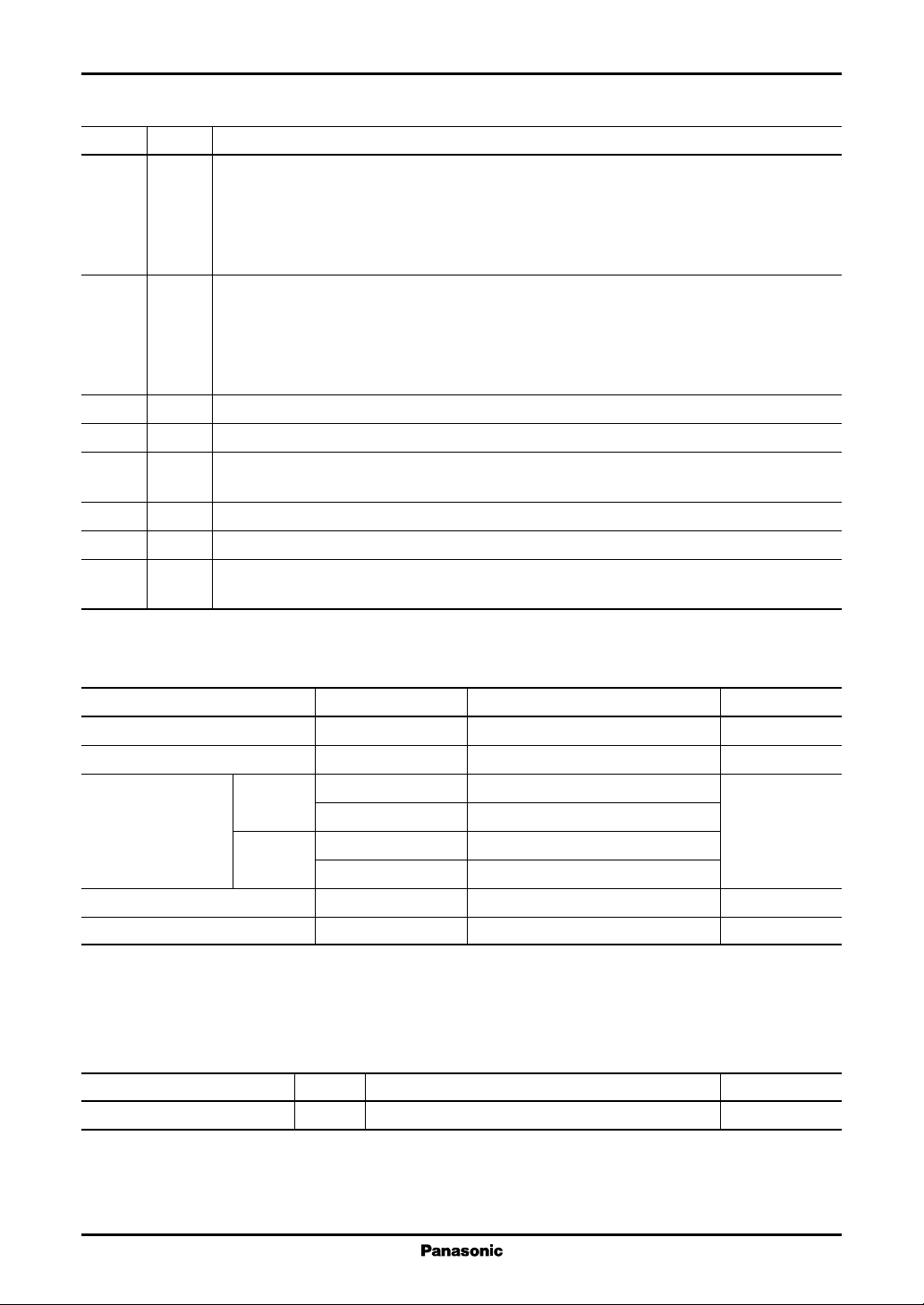
■ Absolute Maximum Ratings
Parameter Symbol Rating Unit
Supply voltage V
Peak output current I
CC
OP
28 V
−1, +2A
Power dissipation AN8038 PD (Ta = 25°C) 500 mW
(Independent IC PD (Ta = 85°C) 260
1
without a heat sink) AN8038S PD (Ta = 25°C) 306
PD (Ta = 85°C) 122
Operating temperature T
Storage temperature T
Note) *1: When mounted on a printed circuit board: 477 mW
2: When mounted on a printed circuit board: 191 mW
*
opr
stg
*
2
*
−30 to +85 °C
−55 to +150 °C
■ Recommended Operating Range
Parameter Symbol Range Unit
Supply voltage V
From the stop voltage to the OVP operating voltage V
CC
3

AN8038, AN8038S Voltage Regulators
■ Electrical Characteristics at VCC = 18 V, Ta = 25°C
Parameter Symbol Conditions Min Typ Max Unit
Low voltage protection (U.V.L.O.) Start V
initial startup supply voltage.
Low voltage protection (U.V.L.O.) Stop V
operation stop supply voltage
Overvoltage protection (OVP) OVP V
operating supply voltage
Overvoltage protection (OVP) OVPC V
release supply voltage
Overvoltage protection (OVP) OVP I
operating time circuit current 1
Overvoltage protection (OVP) OVP I
operating time circuit current 2
Transformer reset detection (TR) TR V
threshold voltage
Transformer reset detection (TR) TR V
upper limit clamp voltage
Transformer reset detection (TR) TR V
lower limit clamp voltage
Transformer reset detection (TR) TR I
pin source current
Overcurrent protection (CLM) CLM V
threshold voltage
Oscillator (CF) maximum CF GI
on-period current gain
Oscillator (CF) maximum CF I
on-period current
Oscillator (CF) minimum CF I
off-period current 1
Oscillator (CF) minimum CF I
off-period current 2
Output oscillator frequency f
Standby pin (RSTB) voltage V
Standby operation (RSTB) RSTB V
threshold voltage
Current feedback pin (IFB) voltage V
Pre-startup low-level output voltage STB V
Low-level output voltage V
High-level output voltage V
Circuit current during startup 1 I
START1
Circuit current 1 OPR1 I
Circuit current 2 OPR2 I
4
CC
CC
CC
CC
CC1
CC2
TH
CLHITR
CLLITR
TR
TH
ONIFB
ON
OFF1IIFB
OFF2IIFB
OSC
RSTB
TH
IFB
OL
OL
OH
CC1VCC
CC2VCC
VCC = 22 V → 10 V 0.4 0.53 0.66 mA
VCC = 22 V → 18 V 1.3 1.7 2.1 mA
= 1 mA 1.2 1.5 1.8 V
= −1 mA − 0.3 − 0.15 0 V
VTR = 0.5 V −50µA
= Open 0.8 1.0 1.2
ITR = 0 mA 210 280 350 µA
= − 0.7 mA −1 560 −1 250 −940 µA
= −1.3 mA −70 −55 −40 µA
CF = 1 000 pF, ITR = −450 µA 105 140 175 kHz
I
= − 0.5 mA
IFB
I
= − 0.7 mA 5 5 .6 6 .2 V
IFB
VCC = 12 V 1.0 1.25 V
I
= 0.2 A 0.9 2.0 V
OUT
I
= − 0.1 A 15.5 16.3 V
OUT
= 10 V 6.1 8.7 11.3 mA
= 18 V 6.4 9.1 11.8 mA
12.9 14.4 15.9 V
8.0 8.9 9.8 V
18.7 20.5 22.3 V
6.6 7.5 8.4 V
0.15 0.25 0.35 V
−225 −205 −185 mV
3.2 3.5 3.8 V
0.3 0.5 0.7 V
120 190 280 µA
Voltage Regulators AN8038, AN8038S
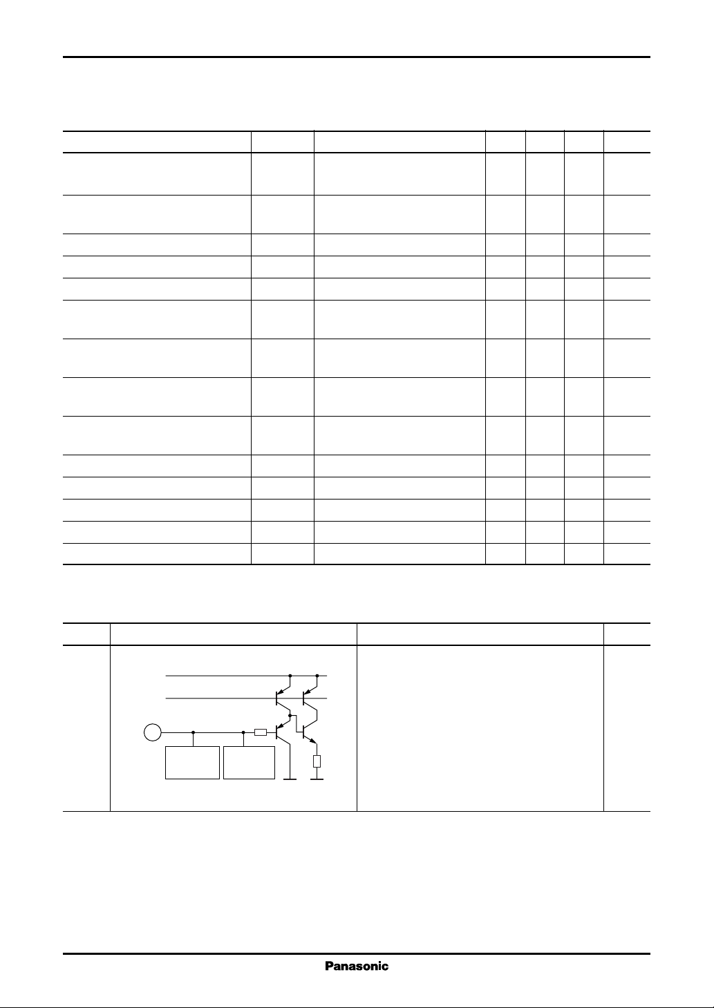
■ Electrical Characteristics at VCC = 18 V, Ta = 25°C (continued)
•
Design Reference Data
Note) The characteristics listed below are theoretical values based on the IC design and are not guaranteed.
Parameter Symbol Conditions Min Typ Max Unit
Low-voltage protection (U.V.L.O.) ∆V
start/stop supply voltage difference
Transformer reset (TR) detection TR ∆V
threshold hysteresis width
Oscillator (CF) upper limit voltage V
Oscillator (CF) lower limit voltage 1 V
Oscillator (CF) lower limit voltage 2 V
Maximum on-period t
Minimum off-period 1 t
Minimum off-period 2 t
Light-load oscillator frequency f
CLH
CFL1
CFL2
ON(max)
OFF(min)1IIFB
OFF(min)2IIFB
OSC2
Output rise time t
Output fall time t
TR output response time t
CLM output response time t
Circuit current during startup 2 I
TR
CLM
START2
CC
TH
I
= − 0.5 mA, CF = 1 000 pF 4.2 V
IFB
I
= − 0.5 mA, CF = 1 000 pF 1.0 V
IFB
I
= − 0.2 mA, CF = 1 000 pF 0.1 V
IFB
I
= − 0.2 mA, CF = 1 000 pF 12 µs
IFB
VTR = 0.1 V
= − 0.2 mA, CF = 1 000 pF 2.6 µs
VTR = 0.1 V
= −1.3 mA, CF = 1 000 pF 67 µs
ITR = −450 µA
I
= −1.3 mA, CF = 1 000 pF 15 kHz
IFB
ITR = −450 µA
r
f
10% to 90%, I
10% to 90%, I
= 0 mA 40 ns
OUT
= 0 mA 20 ns
OUT
Ta = −30°C to +85°C 100 190 300 µA
5.4 V
0.1 V
400 ns
100 ns
■ Terminal Equivalent Circuits
Pin No. Equivalent Circuit Description I/O
1 TR: I
V
REF
7 V
TR
1
High-side
clamp
Low-side
clamp
Transformer reset detection input.
When a transformer reset is detected, i.e., a low
level is input to this pin, the IC output goes high.
However, the transformer reset signal is ignored
if the signal is shorter than the minimum offperiod determined by the C
pin. Also note that
F
the maximum on-period is corrected according
to the source current.
5
AN8038, AN8038S Voltage Regulators
■ Terminal Equivalent Circuits (continued)
Pin No. Equivalent Circuit Description I/O
2 RSTB:
Adjusts the light-load detection level that deter-
V
REF
17.5 kΩ
RSTB
Comp.
CF
17.5 kΩ
2
mines the time when the IC switches from RCC
to discontinuous operation. When the voltage
which is I-V conversion of current feedback signal goes up higher than this pin, operating frequency is reduced.
An arbitrary level can be set by inserting an
external pull-down resistor.
3 CF:
V
REF
I
OFF
Connection for the capacitor that determines the
on- and off-periods of the IC output (Out).
Comp.
The on- and off-periods are corrected by I
which is proportional to the flowing out cur-
V
FB
I
3
ON
rent at the TR pin, and I
to the current at IFB pin.
which corresponds
OFF
ON
CF
4 IFB: I
V
REF
× 5× 1
Connection for the photocoupler used for the
power supply output error-voltage feedback.
This input can decrease the photocoupler dark
V
FB
20 kΩ 1 kΩ
current by about 250 µA.
4
IFB
5 CLM: I
V
REF
Input to the pulse-by-pulse overcurrent protection circuit. Normally, we recommend adding
Comp.
an external filter for this input.
5
CLM
6 GND:
GND
6
IC ground.
6
Voltage Regulators AN8038, AN8038S
■ Terminal Equivalent Circuits (continued)
Pin No. Equivalent Circuit Description I/O
7V
V
CC
:I
OUT
Output used to directly drive a power MOSFET.
A totem pole structure is adopted in this output
circuit.
The absolute maximum ratings for the output
7
V
OUT
current are:
Peak: +2 A, −1 A
DC: +200 mA, −100 mA
8V
V
CC
8
:
CC
Power supply.
This pin monitors supply voltage and has the
threshold for the start, stop, OVP, and OVP
reset levels.
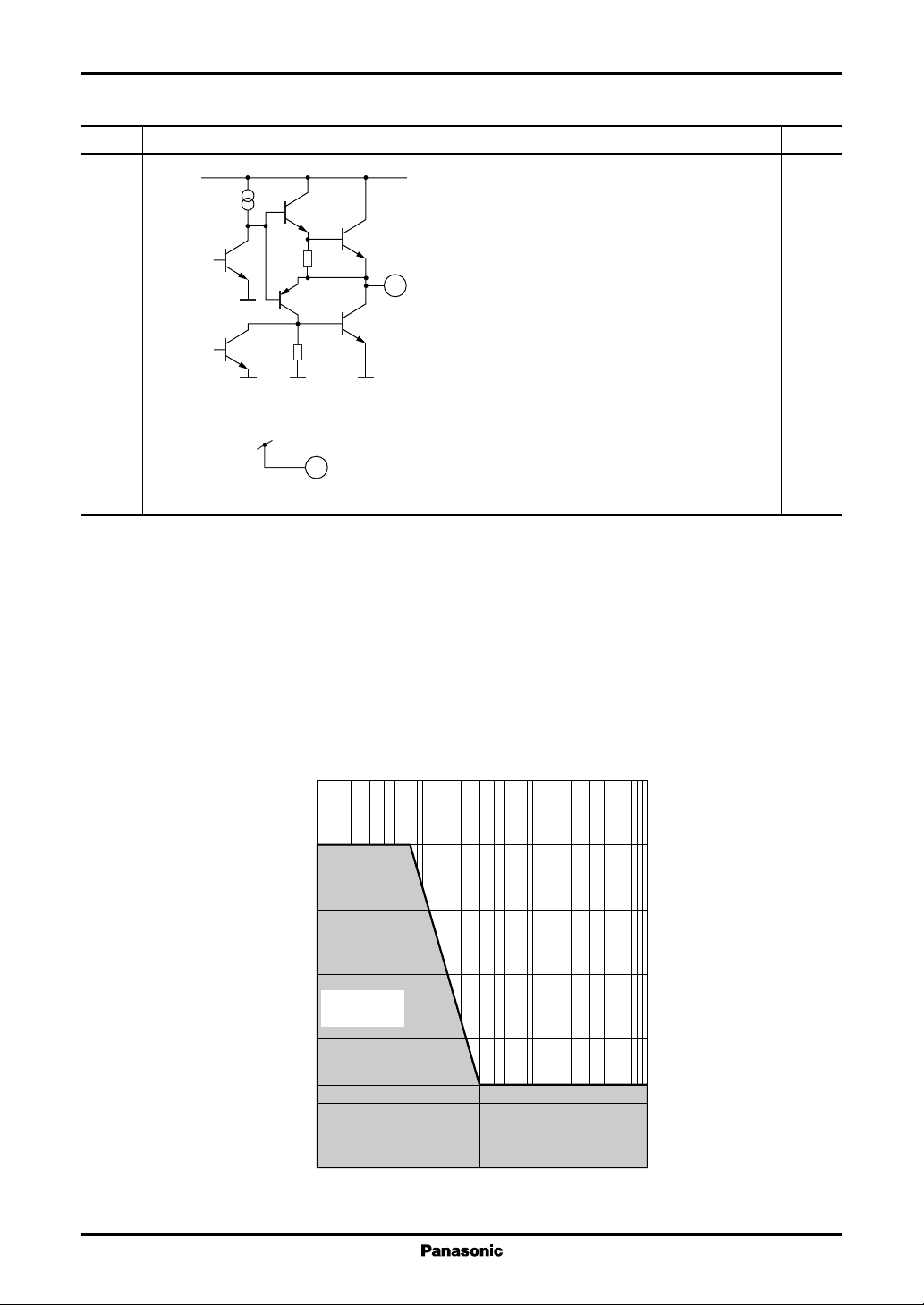
■ Usage Notes
The circuit current during startup is set to a low level to minimize power loss due to the startup resistor. However,
V
ripple caused by the power transistor switching on and off may result in incorrect operation of the U.V.L.O. circuit
CC
and failure to start.
The figure shows the allowable range for V
V
ripple so that it remains within the allowable range.
CC
ripple. Insert a capacitor near the IC's V
CC
and GND pins to reduce
CC
3
2.5
2
1.5
ripple amplitude (V[p-p])
1
CC
V
0.6
0.5
0
Recommended
operating range
10
Allowable VCC ripple range
70 100 300 1 000 10 000
VCC ripple frequency (kHz)
7
 Loading...