

Panasonic AN8037, AN8027 Datasheet
Voltage Regulators
AN8027, AN8037
AC-DC switching power supply control IC with standby mode
■ Overview
The AN8027 and AN8037 are ICs developed for self-
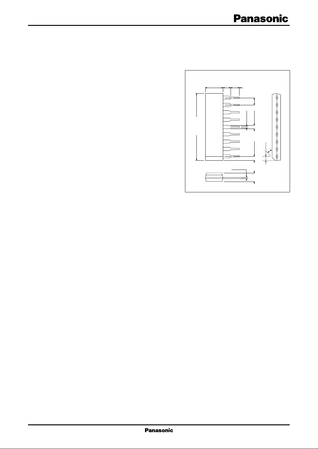
6.0±0.3
2.4±0.25
3.3±0.25
Unit: mm
excited switching regulator of RCC local resonance control type.
These ICs are designed to achieve stability and high
efficiency over a wide input voltage range and loads range
(light loads to heavy loads), for supporting input levels
used worldwide and improved conformance with energy
conservation laws.
■ Features
• Support improved conformance with energy conserva-
tion laws by providing two operating modes.
• Standby mode (light loads):
Achieves better efficiency due to reduced frequency .
• Normal mode:
23.3±0.3
9
8
7
6
5
4
3
2
1
SIP009-P-0000C
0.3
+0.1
–0.05
0.5±0.1
2.54
1.5±0.25
1.5±0.25
3.0±0.3
30°
1.4±0.3
Achieves high efficiency in RCC local resonance operation with zero-cross detection.
• Incorporating an input voltage compensation function available to a wide input range for worldwide use.
• This function compensates the maximum on-period in inverse proportion to the input voltage.
• Incorporating a timer latch function.
• The time period can be adjusted according to the overload in normal mode or standby mode.
• This function makes it possible to protect the IC from damage that may be caused by the short-circuiting of the IC's
external capacitor for the timer.
• Incorporating an overvoltage protection function. (detects at V
CC
pin)
• Incorporating a pulse-by-pulse overcurrent protection function, which makes latch protection possible at the time of
the short-circuiting of the transformer's primary winding.
• Adopting a 9-pin single inline package (E-9S: available to manufacturing in overseas).
• AN8027: Transformer resetting is detected from the high- or low-level signal on the TR pin.
• AN8037: Transformer resetting is detected from the falling edge of the high-level signal on the TR pin.
Refer to the "[1] operation descriptions 7. local resonance operation" section in the application notes.
■ Applications
• Televisions, VCRs, facsimiles, and printers
1
AN8027, AN8037 Voltage Regulators
■ Block Diagram
CC
V
7
INIT
Current
reviser (IFB)
High-side
clamp
Start
Stop
V
REF
Q
Q
7.1 V
Q
Q
Q
Out
Drive
6
In
Out
In
5
GND
SD
OCP
8
2
OVP
Timer
3.8 V
0.5 V
(SD latch)
RS
Q
Q
CF
latch
Q
T
ON
S
T
OFF
R
R
To timer
− 0.2 V
4
CLM
3
FB
TR
9
High-side
1
Low-side
(− 0.15 V)
I/V
conv.
(0.7 V)
clamp
clamp
reviser (I
0.35 V
V
FB
Current
One
shot
Start
pulse
1.0 V
)
TR
CF
■ Absolute Maximum Ratings
Parameter Symbol Rating Unit
Supply voltage V
Constant output current I
Peak output current I
TR pin allowable application current I
OCP pin allowable application voltage V
CLM pin allowable application voltage V
SD pin allowable application voltage V
FB pin allowable application current I
Power dissipation (Ta ≤ 25°C) P
CC
OUT
OP
TR
OCP
CLM
SD
FB
D
Power dissipation (Ta = 85°C) 454 mW
Operating ambient temperature
Storage temperature
Note) 1. *: Except for the operating ambient temperature and storage temperature, all ratings are for Ta = 25°C.
2. Do not apply external currents or voltages to any pins not specifically mentioned.
For circuit current, '+' denotes current flowing into the IC, and '−' denotes current flowing out of the IC.
*
*
T
opr
T
stg
24 V
±150 mA
±1 000 mA
±5mA
− 0.3 to +7.0 V
− 0.3 to +7.0 V
− 0.3 to +7.0 V
0 to −2.0 mA
874 mW
−30 to +85 °C
−55 to +150 °C
■ Recommended Operating Range
Parameter Symbol Range Unit
Supply voltage V
2
From the stop voltage to the OVP supply voltage V
CC

Voltage Regulators AN8027, AN8037
■ Electrical Characteristics at VCC = 18 V, Ta = 25°C
Parameter Symbol Conditions Min Typ Max Unit
Low voltage protection (U.V.L.O.) V
initial startup supply voltage
Low voltage protection (U.V.L.O.) V
operation stop supply voltage
Overvoltage protection (OVP) V
operating supply voltage
Overvoltage protection (SD) V
operating threshold voltage
Overvoltage protection (SD) V
reset threshold voltage
Remote (RM) operating V
threshold voltage
Shutdown (SD) standby voltage V
Overvoltage protection (OVP) V
reset supply voltage
Remote (RM) operating time I
circuit current
Overvoltage protection (SD) I
operating time circuit current 1
Overvoltage protection (SD) I
operating time circuit current 2
Timer latch (SD) charge current 1 I
Timer latch (SD) charge current 2 I
Timer latch (SD) start feedback I
current
Transformer reset detection (TR) V
threshold voltage
Transformer reset detection (TR) V
upper limit clamp voltage
Transformer reset detection (TR) V
lower limit clamp voltage
Overcurrent protection (CLM) V
threshold voltage
Oscillator (CF) upper limit voltage
Oscillator (CF) lower limit voltage 1
Oscillator (CF) lower limit voltage 2
Oscillator (CF) maximum G
on-period current gain
Oscillator (CF) maximum I
on-period current
Oscillator (CF) minmum I
off-period current 1
CC-START
CC-STOP
CC-OVP
TH1-SD
TH2-SD
TH1-RM
STB-SD
CC-OVPC
CC-RMVCC
CC1-SDVCC
CC2-SDVCC
SD1-TIM
SD2-TIM
FB-TIMITR
TH-TR
CLH-TRITR
CLL-TRITR
TH-CLM
V
V
V
ION-CF
ON-CFITR
OFF1-CFIFB
SD pin = Open 1.0 1.5 2.0 V
FB pin = Open, ITR = −270 µA 68 102 136 µA
FB pin = Open, ITR = −1.64 mA 179 267 355 µA
FB pin = Open, CF = 2 200 pF 3.8 4.2 4.6 V
H-CF
FB pin = Open, CF = 2 200 pF 0.8 1.0 1.2 V
L1-CF
L2-CFIFB
FB pin = Open, ITR = −750 µA 0.8 1.0 1.2
= 18 V, VSD = 0 V 3.0 4.0 5.0 mA
= 10 V, VSD = 4.3 V → Open 1.2 1.5 1.8 mA
= 18 V, VSD = 4.3 V → Open 3.6 4.5 5.4 mA
= −1 mA, R
= 30 kΩ− 0.95 − 0.75 − 0.55 mA
OCP
= 3 mA 0.55 0.7 0.85 V
= −3 mA − 0.3 − 0.15 0 V
= − 0.5 mA, CF = 2 200 pF 0 0.1 0.3 V
= 0 mA 200 250 300 µA
= − 0.4 mA −880 −660 −440 µA
13.4 14.9 16.4 V
7.7 8.6 9.5 V
19.4 20.5 21.6 V
3.5 3.9 4.3 V
0.4 0.8 1.2 V
0.05 0.15 0.3 V
7.3 8.1 8.9 V
0.15 0.25 0.35 V
−220 −200 −180 mV
3

AN8027, AN8037 Voltage Regulators
■ Electrical Characteristics at VCC = 18 V, Ta = 25°C (continued)
Parameter Symbol Conditions Min Typ Max Unit
Oscillator (CF) minmum I
OFF2-CFIFB
off-period current 2
Minimun off-period threshold I
FB-TOFF
feedback current
Overcurrent protection (OCP) pin I
OCP-OCP
source current
Output oscillator frequency F
Pre-startup low-level output voltage V
Low-level output voltage V
High-lebel output voltage V
Pre-startup circuit current 1 I
Circuit current 1 I
Circuit current 2 I
Circuit current durring startup 1 I
CC-STB1VCC
CC1-OPR1VCC
CC2-OPR2VCC
START1
OSC
OL-STBVCC
OLIOUT
OHIOUT
= − 0.8 mA −210 −160 −110 µA
− 0.78 − 0.6 − 0.42 mA
−130 −100 −70 µA
CF = 2 200 pF, ITR = 475 µA, 50 65 80 kHz
IFB = − 0.5 mA
= 13.5 V, I
= 1 mA 1.0 1.25 V
OUT
= 0.1 A 0.9 2.0 V
= − 0.1 A 15.5 16.3 V
= 13.5 V 75 100 125 µA
= 10 V 8.5 11.5 14.5 mA
= 18 V 9.0 12.0 15.0 mA
200 380 µA
• Design reference data
Note) The characteristics listed below are theoretical values based on the IC design and are not guaranteed.
Parameter Symbol Conditions Min Typ Max Unit
Low voltage protection (U.V.L.O.) ∆V
CC
6.3 V
start/stop supply voltage difference
Remote (RM) reset threshold voltage V
Timer latch (SD) overcurrent T
TH2-RM
CLM-SD
0.1 V
0.1 s
protection time
Transformer reset detection (TR) ∆V
TH-TR
0.05 V
threshold hysteresis width
Maximum on-period T
Minimum off-period T
Overcurrent protection (OCP) T
ON(max)ITR
OFF(min)ITR
SD(ON)-OCPIFB
= 0 mA, IFB = − 0.2 mA 26.5 µs
= 0 mA, IFB = − 0.2 mA 5 µs
= − 0.5 mA, R
= 22 kΩ1.8 µs
OCP
power-on charge period
Overcurrent protection (OCP) T
SD(OFF)-OCPIFB
= − 0.5 mA, R
= 30 kΩ8.8 µs
OCP
power-off charge period
Output rise time t
Output fall time t
TR output response time T
CLM output response time T
Pre-startup circuit current 2 I
CC-STB2
CLM
r
f
TR
10% to 90%, I
10% to 90%, I
= 0 mA 60 ns
OUT
= 0 mA 20 ns
OUT
800 ns
100 ns
VCC = 13.5 V, 50 1 0 0 150 µA
Ta = −30°C to +85°C
Only for AN8037
Timer period during startup T
START
100 µs
4
Voltage Regulators AN8027, AN8037
V
REF
V
FB
I
OFF
I
ON
Comp.
3
■ Pin Descriptions
Pin No. Pin name I/O Explanation Equivalent Circuit
1 TR I Transformer reset detection input. When the
IC detects transformer resetting and the falling edge of a high-level signal is input to
this pin of the AN8037 or a low-level signal
is input to the same pin of the AN8027, the
level of the Out pin becomes high. However,
the transformer reset signal is ignored if the
signal is shorter than the minimum off-period determined by the CF pin. Also note
that the maximum on-period is corrected according to the source currents.
2 OCP Connection for the resistor that determines
the overload level of the IC to activate the
timer latch protection circuit.
By judging the operating mode (i.e., the normal or standby mode) of the IC from the
secondary side, the timer period is adjusted
with the selection of external resistance according to the operating mode.
3CF Connection for the capacitor that determines
the on- and off-periods of the IC output (Out).
The on- and off-periods are corrected by I
which is proportional to the flowing out current at the TR pin, and I
which corre-
OFF
sponds to the current at FB pin.
ON
V
V
REF
1
REF
High-side
clamp
Comp.
Low-side
clamp
CF
2
4 CLM I Input to the pulse-by-pulse overcurrent pro-
tection circuit.
Normally, we recommend adding an external
filter for this input. If overcurrent continues
V
REF
Comp.
for several cycles, the IC determines that the
operation is erroneous, thus triggering the
latch protection function.
CLM(−)
4
5 GND IC ground.
5
5
AN8027, AN8037 Voltage Regulators
■ Pin Descriptions (continued)
Pin No. Pin name I/O Explanation Equivalent Circuit
6 Out O Output used to directly drive a power MOSFET.
A totem pole structure is adopted in this
output circuit.
The absolute maximum ratings for the output
current are:
Peak: ±1 A
DC: ±150 mA
7VCC Power supply.
This pin monitors supply voltage and has the
threshold for the start, stop, OVP, and OVP
reset levels.
8 SD I This pin is used in RM (remote), OVP (over-
voltage protection), and timer latch.
RM:
The IC is in remote operation if this pin is
short-circuited to the ground and the output
of the IC is turned off.
OVP:
When overvoltage signal of the power supply is detected and high is inputted to the terminal, it turns off the internal circuit. At the
same time, it holds that condition (latch).
Timer latch:
It detects the output voltage fall due to the
overcurrent condition of the power supply
output through the current level inputted to
FB. When the I
decreases under the current
FB
of certain value, the charge current flows in
the capacitor which is connected to this terminal. Then, when the capacitor is charged
up to the threshold voltage of the OVP, the
OVP works so that the IC could keep the operation stop condition.
9 FB I Connection for the photocoupler used for the
power supply output error-voltage feedback.
This input can decrease the photocoupler dark
current by about 200 µA.
V
CC
V
OVP
RM
V
CC
Comp.
Comp.
REF
V
FB
3.9 V
0.1 V
7
I
25 µA
6
TIM
8
9
I
FB
6
Voltage Regulators AN8027, AN8037
■ Application Notes
[1] Operation descriptions
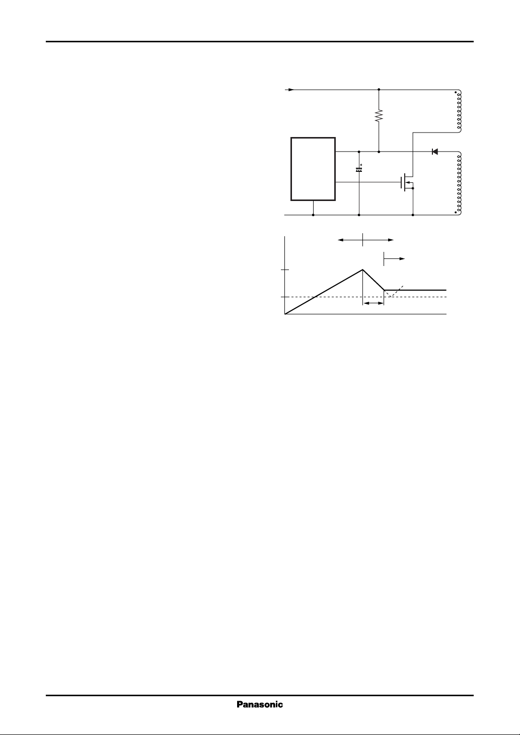
1. Start/stop circuit block
• Startup mechanism
After the AC voltage is applied and the
supply voltage due to the current in the startup
resistor reaches the startup voltage and the IC
begins to operate, drive of the power MOSFET
begins. This causes a bias in the transformer, and
the supply voltage is provided to the IC from
the bias winding. (This is point a in figure 1.)
During the period between the point when the
startup voltage is reached, and the point when
the bias winding can generate a voltage enough
to supply the IC, the IC supply voltage is provided by the capacitor (C8) connected to V
Since the supply voltage falls during this period
(area b in figure 1), if the supply voltage falls
below the IC stop-voltage before an adequate
supply voltage can be provided by the bias winding, it will not be possible to start the power sup-
CC
.
Startup
voltage
Stop
voltage
ply. (This is the state at point c in figure 1.)
• Functions
This IC includes a function that monitors the V
CC
voltage (14.9 V typical), and stops operation when the voltage falls below the stop voltage (8.6 V typical). Since
a large voltage difference (6.3 V typical) is taken between the start and stop voltages, it is easy to select values for
the start resistor and the capacitor connected to V
Note) To start up the IC operation, the startup current which is a pre-start current plus a circuit drive current is necessary.
Set the resistance value so as to supply a startup current of 400 µA.
CC
Rectified AC
Startup resistor
R1
V
CC
C8
V
OUT
GND
StartupStandby
Voltage supplied
a
from bias winding
Startup state
c
b
Startup failure
Figure 1
voltage. It starts IC operation when VCC reaches the startup
.
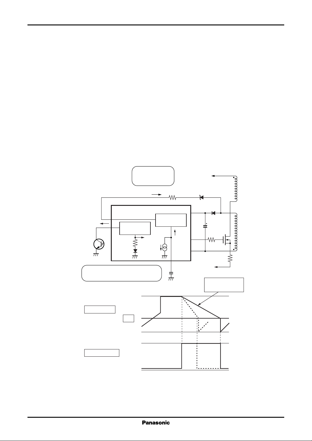
2. Oscillation circuit
The oscillation circuit makes use of the charge and discharge of current to and from the capacitor C
connected
CF
to the CF pin (pin 3) to determine the switching timing of the power MOSFET.
The IC is in constant voltage control by changing the on-period of the power MOSFET without making offperiod change while the IC is in normal (RCC continuous) operation mode. At that time, the on-period is controlled by directly changing the output pulse width of the oscillation circuit, and the maximum on-period can be
adjusted with input voltage compensation by detecting the input voltage with the flow of current from the TR pin
(TR source current). Refer to figure 2. When the IC is in standby mode (for light loads), the stable, efficient
control of the IC is ensured by detecting the flow of current from the FB pin (I
) and changing the off-period for
FB
a decrease in frequency. Refer to figure 3.
The following provides information on how to set on- and off-period.
• Setting the on-period
The output on-period is the discharge period when the CF pin is between the peak value oft V
(typical) and V
.
FB
H-CF
An approximate on-period of the power MOSFET is obtained from the following formula. Refer to figure 2.
T
= CCF × (V
ON
whereas, V
− VFB)/I
H-CF
H-CF
I
= I
ON
I
= (EIN × NB/NP − VZ)/R
TR
ON
= 4 V typ.
+ 250 µA typ.
TR
VFB = 0.7 V typ. (I
V
= 4 kΩ × IFB typ. (I
FB
≤ 200 µA)
FB
FB
TR
> 200 µA)
= 4 V
7
AN8027, AN8037 Voltage Regulators
■ Application Notes (continued)
[1] Operation descriptions (continued)
2. Oscillation circuit (continued)
• Setting the on-period (continued)
TON: On-period
C
: Value of a capacitor connected to CF pin
CF
V
: Voltage internally converted from feedback signal I
FB
V
: CF upper limit voltage
H-CF
I
: On-period discharge current
ON
I
: Flowing current at TR pin
TR
E
: Voltage on primary winding
IN
NB : Number of turns in the bias winding
NP : Number of turns in the primary winding
V
: Voltage on Zener diode connected to bias winding
Z
R
: Value of a resistor connected to the TR pin
TR
The power MOSFET is turned off if the voltage at the CLM pin reaches the pulse-by-pulse overcurrent
protection threshold voltage (i.e., −200 mV typical) when the overcurrent protection function of the IC is
operating.
TON is shortened
because large E
increases I
.
TR
I
TR
IN
R
TR
FB
E
IN+
V
Z
NP
AN8027, AN8037
TR
I
FB
PC
The minimum current is guaranteed
to prevent a limitless increase in T
CF pin voltage
FB
Current mirror
20 kΩ
= 4 V
V
H-CF
V
1 : 5
FB
V
FB
250 µA
Current mirror
ITR=I
typ.
.
ON
ON
CF
V
I
ON
Out
GND
C
CF
0 V
VCC − 1.5 V
Out pin voltage
Off On
0 V
Figure 2. On-period block diagram and control waveform
CC
E
IN−
EIN; large
I
TR(ION
NB
); large
The maximum on-period can be used for overcurrent protection.
When the input voltage is low, the maximum on-period overcurrent protection is possible.
When the input voltage is high, the CLM pulse-by-pulse overcurrent protection is possible.
8
Voltage Regulators AN8027, AN8037
■ Application Notes (continued)
[1] Operation descriptions (continued)
2. Oscillation circuit (continued)
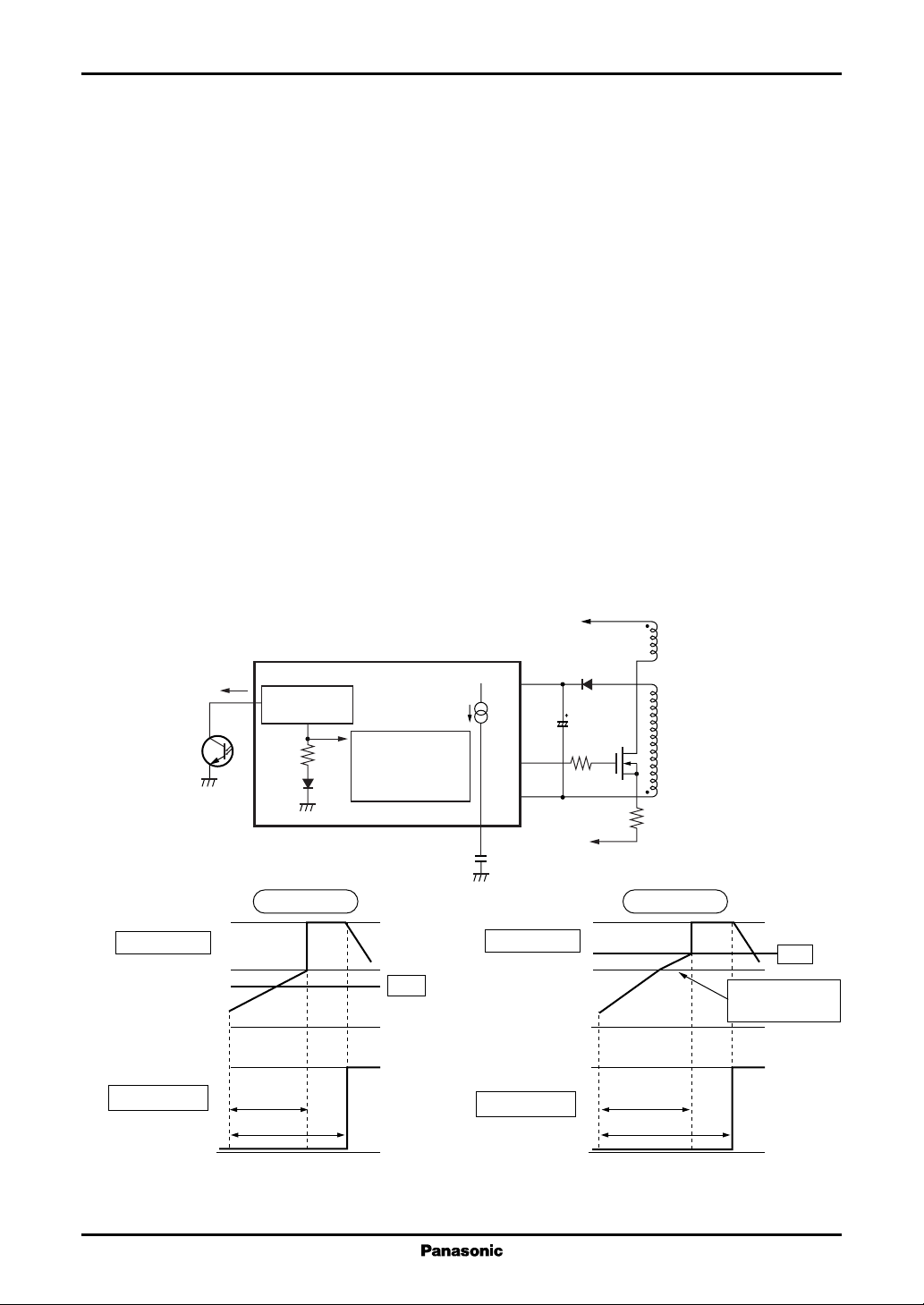
• Setting the off-period
The minimum off-period is the charge period from V
An approximate minimum off-period of the power MOSFET is obtained from the following formula.
Refer to figure 3.
T
T
C
V
V
I
OFF1
I
OFF2
= CCF × V
OFF(min)
= {C
V
TH(OFF)
I
OFF1
I
OFF2
: Minimum off-period
OFF(min)
: Value of a capacitor connected to the CF pin
CF
: Voltage internally converted from feedback signal I
FB
: Threshold voltage of VFB to extend off-period
TH(OFF)
TH(OFF)/IOFF1
× V
CF
TH(OFF)
= 2.4 V typ.
= 660 µA typ.
= 160 µA typ.
(I
≤ 0.6 mA)
FB
/ I
} + {CCF × (VFB − V
OFF1
: Charge current until CF pin voltage increases from 0.2 V to 2.4 V
: Charge current until CF pin voltage increases from 2.4 V to V
When the IC is in local resonance operation, the off-period is determined by the longer one of either the
time required for the input voltage on the TR pin to drop below the threshold voltage or the minimum offperiod (T
) specified by the CCF.
OFF(min)
Thus the power MOSFET is in continuous on/off operation.
= 0.2 V (typical) to V
L-CF
) / I
TH(OFF)
E
OFF2
FB
IN+
or VFB .
TH(OFF)
}(IFB > 0.6 mA)
FB
NP
V
H−CF
CF pin voltage
V
= 2.4 V
TH(OFF)
V
= 0.2 V
L2−CF
V
CC
Out pin voltage
= 4 V
0 V
− 1.5 V
0 V
Current mirror
FBPC
20 kΩ
IFB < 0.6 mA
T
OFF(min)
T
OFF
AN8027, AN8037
1 : 5
V
FB
I
= 660 µA typ.
OFF
(I
< 0.6 mA)
FB
I
= 160 µA typ.
OFF
(I
> 0.6 mA)
FB
On
NB
I
OFF
V
Out
CC
GND
CF
C
CF
IFB > 0.6 mA
V
= 4V
H−CF
CF pin voltage
V
V
FB
= 2.4 V
TH(OFF)
= 0.2 V
V
L2−CF
− 1.5 V
V
CC
Out pin voltage
0 V
T
OFF(min)
T
OFF
IFB; large
T
OFF(min)
On
V
FB
; large
0 V
Figure 3. Off-period block diagram and control waveform
9
 Loading...