

Panasonic AN8031 Datasheet
Voltage Regulators
AN8031
Active filter control IC
■ Overview
In supplying electric power from commercial power
6.0±0.3
2.4±0.25
3.3±0.25
Unit: mm
supply to various electrical equipment, there is a possibility that the harmonic distortion generated in the power
line may give obstruction to the power facilities or other
electrical equipment. The use of active filter is one of the
methods to solve the harmonic distortion problems.
The AN8031 is a monolithic IC which incorporates
the control and protection functions into one package so
that the active filter can be constructed easily. It is most
suitable for the measures against the harmonic distortion
problems such as lighting equipment.
■ Features
23.3±0.3
9
8
7
6
5
4
3
2
1
0.3
+0.1
–0.05
0.5±0.1
2.54
1.5±0.25
1.5±0.25
3.0±0.3
1.4±0.3
• Self-excited peak current mode is adapted.
• Built-in protection circuit for preventing the overvolt-
SIP009-P-0000C
age generated under a small load
• Easy constant setting with enlarged dynamic range of multiplier and error amplifier.
• Using totem pole output circuit which allows the power MOSFET to be directly driven.
• Built-in low voltage protection circuit which ensures the on-resistance during the power MOSFET operation.
• Timer circuit is built in for realizing automatic start.
■ Applications
• Lighting equipment and switching power supply equipment
30°
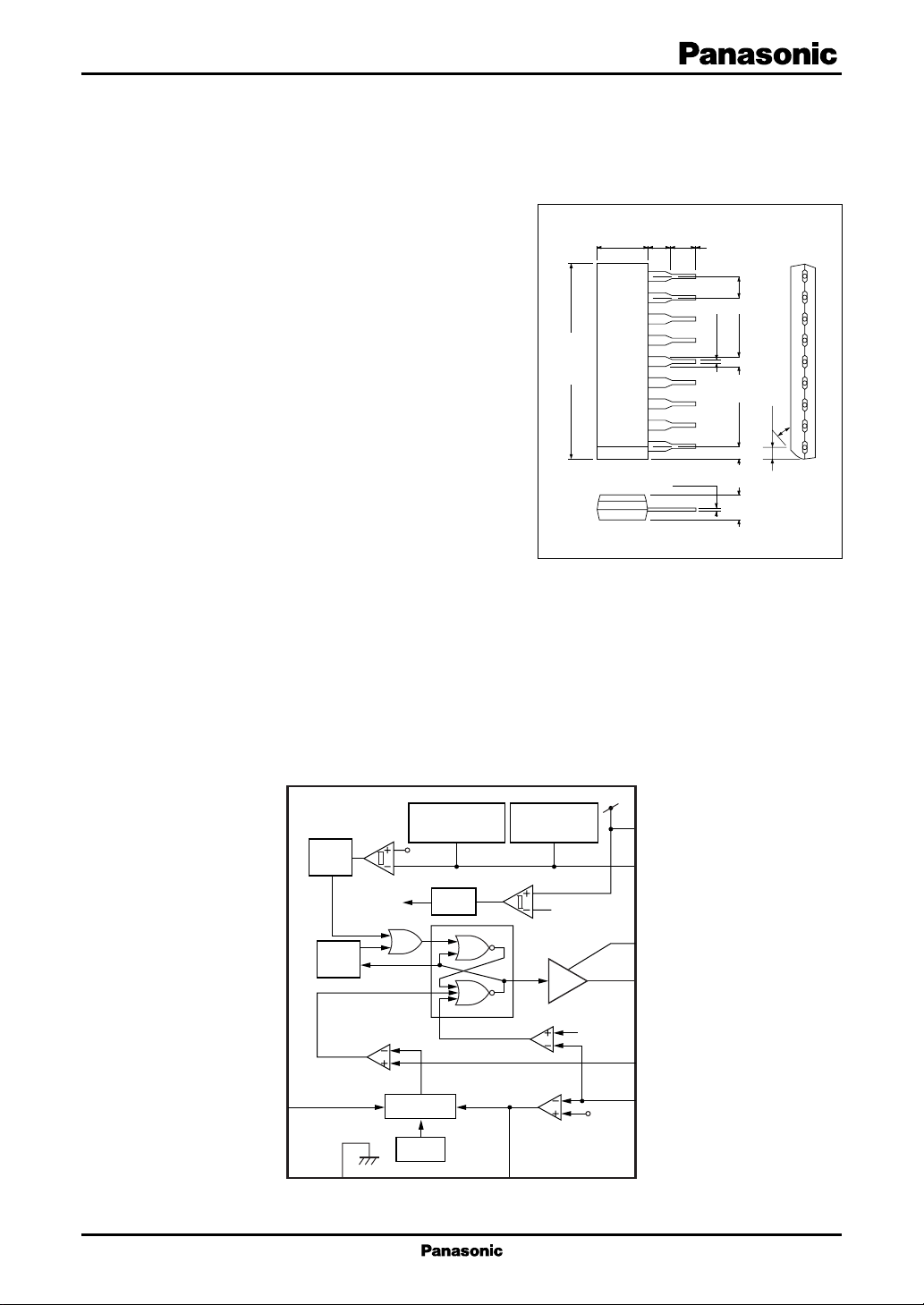
■ Block Diagram
MPI
3
One
shot
Timer
Current
comp.
7
2.5 V
GND
Under voltage
clamper
V
Multiplier
2.5 V
U.V.L.O. comp.
REF
Error amp.
4
Over voltage
clamper
10 V/8 V
Drive
OVP comp.
2.5 V
EO
2.6 V
1
SV
CC
6
V
B
9
PV
CC
8
V
OUT
2
CS
5
EI
1
AN8031 Voltage Regulators
■ Pin Descriptions
Pin No. Symbol Description
1SVCCControl system supply-voltage pin
2 CS Comparator input pin
3 MPI Multiplier input pin
4 EO Error amplifier output pin / multiplier input pin
5 EI Error amplifier inverting input pin / overvoltage protection input pin
6VBTransformer-reset detection pin
7 GND Grounding pin
8V
OUT
9PVCCPower system supply-voltage pin
■ Absolute Maximum Ratings
Parameter Symbol Rating Unit
Supply voltage V
CS allowable application voltage V
MPI allowable application voltage V
EI allowable application voltage V
Output allowable current I
Peak output current I
VB allowable flow-in current I
VB allowable flow-out current I
Power dissipation P
Operating ambient temperature
Storage temperature
Note)*: Expect for the operating ambient temperature and storage temperature, all ratings are for Ta = 25°C.
*
Output pin
*
CC
CS
MPI
EI
O
OP
BI
BO
D
T
opr
T
stg
35 V
− 0.5 to +7V
− 0.5 to +7V
− 0.5 to +7V
±150 mA
±1A
+5mA
−5mA
874 mW
−30 to +85 °C
−55 to +150 °C
■ Recommended Operating Range
Parameter Symbol Range Unit
Supply voltage V
CC
■ Electrical Characteristics at Ta = 25°C
Parameter Symbol Conditions Min Typ Max Unit
Error detection feedback threshold V
voltage 1
Error detection low-level output voltage
Error detection high-level output voltage
Error detection input bias current I
Error detection output supply current I
2
EITH1
V
EOLIEO
V
EOHIEI
EI
EO
0 to 34 V
2.35 2.50 2.65 V
= 0 mA, VEI = 5 V 1.0 1.6 V
= 0 mA, VEI = 0 V 5.0 5 . 7 V
VEI = 0 V − 0.3 −1.0 µA
VEI = 0 V, VEO = 1 V 0.25 0.50 0.75 mA
Voltage Regulators AN8031
■ Electrical Characteristics (continued) at Ta = 25°C
Parameter Symbol Conditions Min Typ Max Unit
Multiplier input D-range (upper limit) V
Multiplier output D-range (upper limit)
V
MPOHVEO
Multiplier gain G
Multiplier input bias current I
Coil detection input threshold voltage V
Coil detection hysteresis width dV
Coil detection high-level clamp voltage
Coil detection low-level clamp voltage
Current detection input offset voltage V
V
V
CSOFF
Current detection input bias current I
Overvoltage detection input V
threshold voltage
V
− V
OVP
EITH1
Low-level output voltage V
High-level output voltage V
Standby output voltage V
OUTLIOUT
OUTHIOUT
OUTSTBIOUT
U.V.L.O. start voltage V
U.V.L.O. stop voltage V
U.V.L.O. start - stop voltage difference
Standby current I
dV
CCSTBVCC
Operation current without load I
MPIHVEO
MP
MPI
BTH
B
BHIB
BLIB
CS
OVP
70 100 130 mV
CCST
CCSP
CC
CC
= 5 V 4.0 4.5 V
= 5 V 4.8 5.4 V
1.0 1.2 1.4 1/V
V
= 0 V −1.5 −3.0 µA
MPI
1.2 1.5 1.8 V
50 100 200 mV
= 5 mA 7.0 7.5 8.0 V
= −5 mA − 0.3 − 0.2 0 V
3.5 15 mV
VCS = 0 V − 0.5 −2.0 µA
2.45 2.60 2.75 V
= 100 mA 0.9 1.5 V
= −100 mA 9.2 10.2 V
= 10 mA 0.8 1.5 V
9.2 10.0 10.8 V
7.0 8.0 9.0 V
dVCC = V
CCST
− V
CCSP
1.75 2.00 2.50 V
= 7 V 40 80 120 µA
VCC = 12 V 6.0 10.0 mA
• Design reference data
Note) The characteristics listed below are reference values based on the IC design and are not guaranteed.
Parameter Symbol Conditions Min Typ Max Unit
Error detection feedback V
EITH2Ta
= −25°C to +85°C 2.3 2.7 V
threshold voltage 2
Error detection open-loop gain G
Error detection gain band width f
Multiplier input D-range (lower limit) V
Multiplier output D-range (lower limit)
Current detection − output delay td
Overvoltage detection − output delay td
Output rise time t
Output fall time t
Timer delay time td
AV
BW
MPILVEO
V
MPOLVEO
CS
OVP
r
f
TIM
= 5 V 0 V
= 5 V 0 V
VCC = 12 V, V
VCC = 12 V, V
= 10% → 90% 50 ns
OUT
= 90% → 10% 50 ns
OUT
85 dB
1.0 MHz
200 ns
500 ns
400 µs
3
AN8031 Voltage Regulators
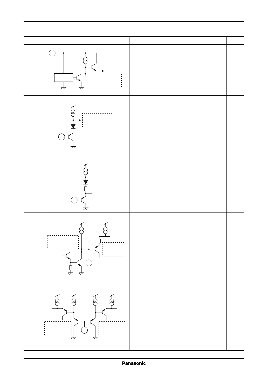
■ Terminal Equivalent Circuits
Pin No. Equivalent circuit Description I/O
1SV
1
:I
CC
The supply voltage terminal for control system.
It monitors the supply voltage and has operating
threshold value for start/stop.
U.V.L.O.
Internal bias
(Approx. 7.1 V)
2 CS: I
Approx. 7.1 V
The input terminal of comparator which detects
To high-speed
converter
the current value flowing in power MOSFET.
The output level of multiplier and the current
value of power MOSFET input from the CS
2
terminal are compared. If the later becomes larger
than the former, the V
is set to low level and
OUT
the power MOSFET output is cut.
3 MPI: I
Approx. 7.1 V
The input terminal of multiplier
The voltage after a full-wave rectified AC input
voltage are monitored.
3
4 EO: O
Approx. 7.1 V Approx. 7.1 V
The output terminal of error amplifier / the input
terminal of multiplier.
Error amplifier
output
Multiplier
input
4
The error amplifier monitors the output voltage
of active filter and amplifies its error portion and
outputs to the multiplier. Therefore, this terminal
serves as another input terminal of the multiplier.
5 EI: I
Approx.
7.1 V
Approx.
7.1 V
Approx.
7.1 V
Approx.
7.1 V
The inverted input terminal of error amplifier / the
overvoltage protection input terminal.
To the noninverted input terminal, the internal
reference voltage of IC (2.5 V typ.) is input.
Since this terminal monitors the output voltage of
Overvoltage
protection input
Error amplifier
5
output
the active filter, it also functions as the input terminal for the overvoltage protector which detects
the overvoltage of output voltage and cuts off the
power MOSFET.
4
Voltage Regulators AN8031
■ Terminal Equivalent Circuits (continued)
Pin No. Equivalent circuit Description I/O
6V
CC
Upper limit
voltage clamp
Approx. 7.1 VPV
Approx. 7.1 V
:I
B
The terminal is connected via the transformer's
sub-coil and resistor. The reset of transformer is
detected and the trigger signal to turn on the power
MOSFET is sent.
6
V
Lower limit
voltage clamp
B
Comparator
input
Since the coil signal of transformer is input as
current, the IC incorporates the circuit which
clamps the upper/lower limit voltage to prevent
malfunction.
7 GND:
7
Grounding terminal
This terminal is used in common for grounding
the control system and the power system.
8V
9
:O
OUT
The output terminal.
It is capable of driving the gate of power MOSFET
directly.
8
9 PV
9
:
CC
The supply voltage terminal for power.
V
B
upper limit
voltage clamp
Power
MOSFET
drive block
It determines the upper limit of output drive voltage. Normally, it is used at the same potential of
SVCC .
5
AN8031 Voltage Regulators
■ Application Notes
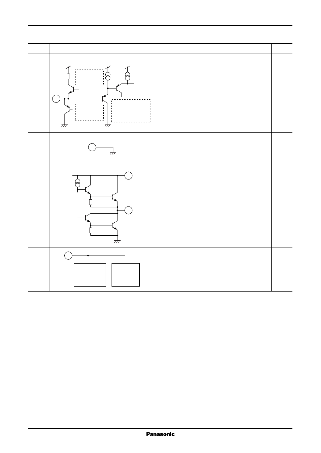
[1] PD Ta curve of SIP009-P-0000C
1 000
900
874
800
700
(mW)
D
600
500
400
Power dissipation P
300
200
100
0
0 25 150
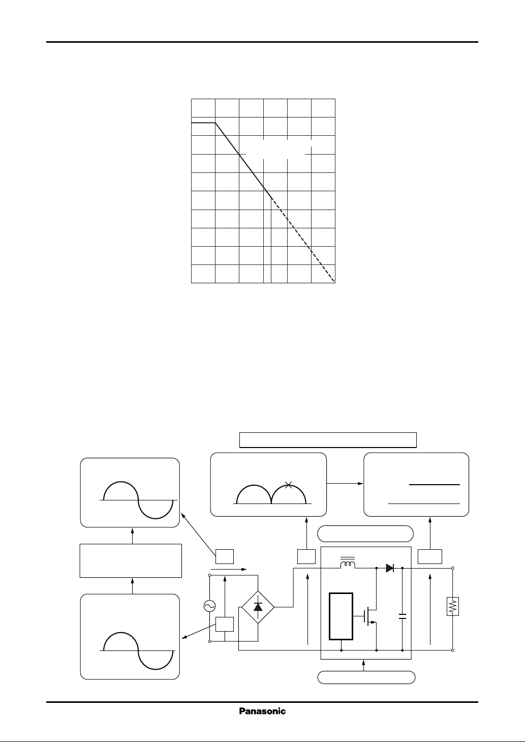
[2] Operation descriptions
1. Normal control
1) Application outline
As shown in figure 1, the standard application of the AN8031 is a booster chopper circuit, which inputs
the voltage rectified from the commercial supply of 100 V/200 V (A in figure 1) and outputs the DC voltage
of 400 V (B in figure 1).
It controls so that the input current proportional to the input voltage (C, D in figure 1) could be flown.
The reason for selecting the output voltage of 400 V is that the withstanding voltage of components and
the operation limitation of booster chopper (input voltage < output voltage) under the worldwide input
voltage are taken into consideration.
PD T
a
Independent IC without a heat sink
R
= 143°C/W
th( j−a)
PD = 874 mW (25°C)
50 75 10085 125
Ambient temperature Ta (°C)
Booster circuit so that set at: E
IN(max)
< E
OUT
D. Input current
0 A
(IIN)
A. Voltage after rectification
)
(E
IN
E
IN(max)
0 V
B. Output voltage (E
400 VDC
0 V
OUT
)
Active filter
Input current proportional
I
IN
E
IN
E
OUT
Output
to input voltage flows.
SBD
C. Input voltage (VIN)
Commercial
power supply (AC)
Input
Load
V
IN
Diode bridge
AN8031
0 V
Booster chopper circuit
Figure 1. Application outline description
6
Voltage Regulators AN8031
■ Application Notes (continued)
[2] Operation descriptions (continued)
1. Normal control (continued)
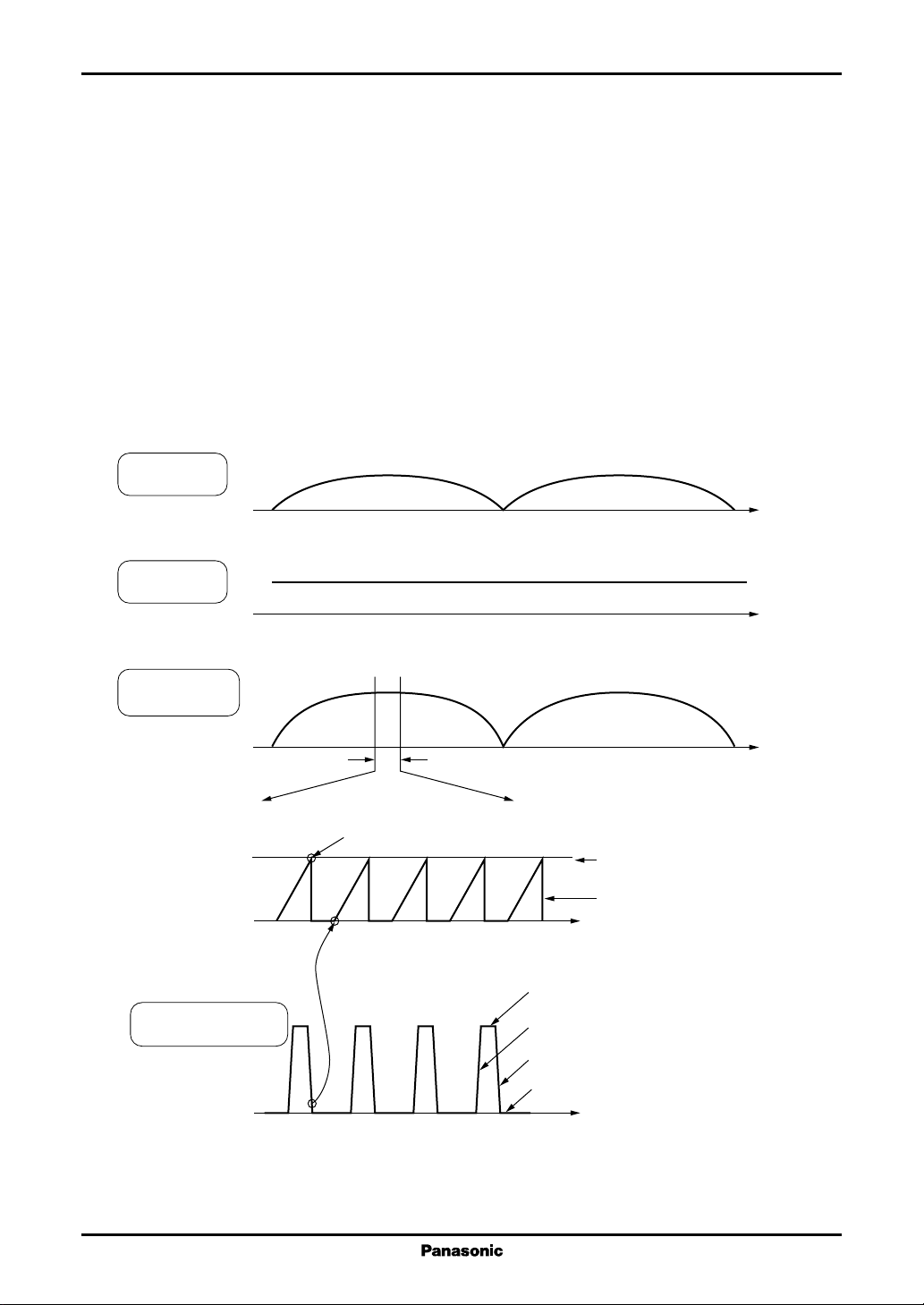
2) Control outline description (Refer to figure 2 and figure 3.)
(1) Input voltage (E
The voltage which is divided from the input voltage of chopper circuit (E
resistor is input to the multiplier input terminal of the AN8031 (MPI terminal).
(2) Output voltage (E
The voltage which is divided from the output voltage of chopper circuit (E
resistor is amplified by the error amplifier of the AN8031 (Input to inverted input terminal (EI terminal))
and input to another multiplier input (EO terminal, which also functions as output for error amplifier).
(3) Multiplication of input voltage and output voltage
The signals input to the multiplier are multiplied and outputted from the multiplier. This output is a
signal which monitors both the input voltage and output voltage of the chopper circuit.
MPI
input voltage
0 V
) detection
IN
) detection
OUT
) by using the external
IN
) by using the external
OUT
Time
EI
input voltage
Multiplier output
(MPO) voltage
Transformer reset
voltage detection (V
Approx. 2.5 V typ.
0 V
0 V
0 V
)
B
0 V
Enlarged
Power MOS turned off
Power MOS turned off
Time
Time
Multiplier output (MPO) voltage
Power MOSFET current detection
(CS) voltage
Time
V
lower limit voltage (regulated inside IC)
B
Power MOS turned on = bias coil voltage
generated
Reset operation of transformer = bias coil
voltage inversion
VB lower limit voltage (regulated inside IC)
Time
Figure 2. Explanation of normal control operation
7
 Loading...