

Panasonic AN8028 Datasheet
Voltage Regulators
AN8028
Self-excited RCC pseudo-resonance type
AC-DC switching power supply control IC
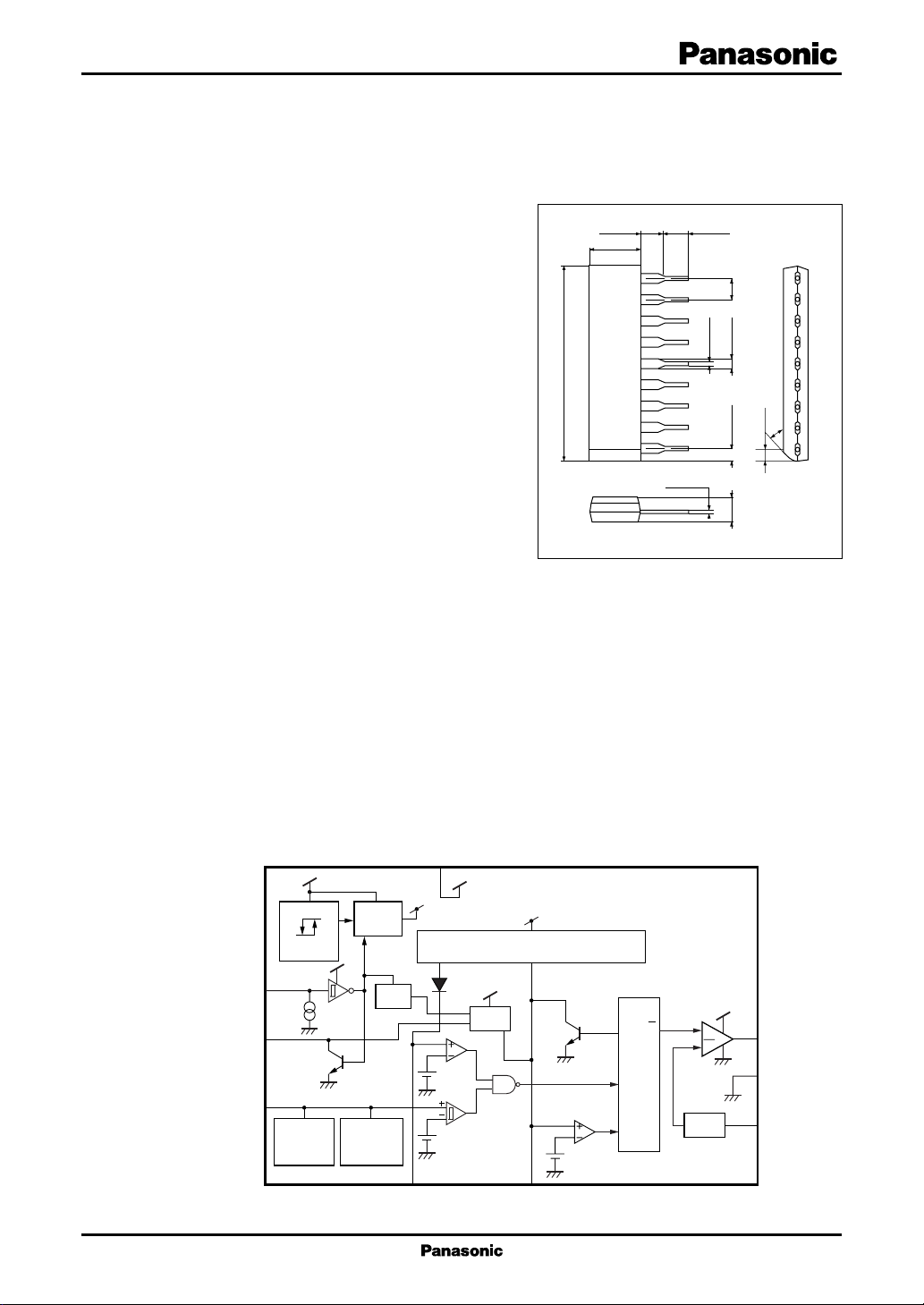
23.3±0.3
2.4±0.25
6.0±0.3
9
8
7
6
5
4
3
2
1
SIP009-P-0000C
+0.1
0.3
–0.05
■ Overview
The AN8028 is an IC developed for controlling the
self-excited switching power supply employing the RCC
pseudo-resonance type control method.
It is compact, equipped only with the necessary minimum functions.
The maximum on-period and the minimum off-period can be set separately by using the external capacitor
and resistor respectively.
It is suitable for the power supply of AV equipment.
■ Features
• Operating supply voltage range:
Stop voltage (8.6 V typical) to 34 V
• Output block employs the totem pole system.
• Power MOSFET can be directly driven.
(output peak current: ±1 A maximum)
• Small pre-start operating current (95 µA typical) allows using a small size start resistor.
• Built-in pulse-by-pulse overcurrent protection function
• Incorporating the protection circuit against malfunction at low voltage (start/stop: 14.9 V/8.6 V)
• Built-in overvoltage protection function (externally resettable)
• Built-in timer latch function
• Equipped with frequency (VF) control function.
• 9-pin single inline package expands the freedom of board design
3.3±0.25
0.5±0.1
2.54
1.5±0.25
1.5±0.25
3.0±0.3
Unit: mm
30°
1.4±0.3
■ Applications
• Televisions, facsimiles, printers, scanners, video equipment
2
TOFF
CC
V
7
Switch
diode
0.1 V
0.32 V
■ Block Diagram
TIM/OVP
FB
TDL
U.V.L.O.
8.6V1.5
8
9
1
Low-side
clamp
0 V
Signal
V
V
REF
(7.1 V)
TIM
High-side
clamp
2.8 V
Current source
I
FB
3
TON
0.7 V
Q
RS
latch
R
S
Q
CLM
6
IN
IN
V
OUT
5
GND
4
CLM
1

AN8028 Voltage Regulators
■ Pin Descriptions
Pin No. Symbol Description
1 TDL Transformer reset detection
2 TOFF Pin for connecting C and R to set minimum off-period
3 TON Pin for connecting C to set minimum on-period
4 CLM Input pin for overcurrent protection detection
5 GND Grounding pin
6V
OUT
7VCCPower supply voltage pin
8 TIM/OVP Pin for use both overvoltage protection circuit and timer latch
9 FB Photocoupler connection pin for error voltage feedback
■ Absolute Maximum Ratings
Parameter Symbol Rating Unit
Supply voltage V
Peak output current I
Power dissipation P
Operating ambient temperature
Storage temperature
Note)*: Expect for the operating ambient temperature and storage temperature, all ratings are for Ta = 25°C.
*
Output pin
*
CC
6PEAK
D
T
opr
T
stg
35 V
±1A
874 mW
−30 to +85 °C
−55 to +150 °C
■ Recommended Operating Range
Parameter Symbol Range Unit
Supply voltage V
CC
■ Electrical Characteristics at VCC = 18 V, Ta = 25°C
Parameter Symbol Conditions Min Typ Max Unit
U.V.L.O. start supply voltage V
U.V.L.O. operation stop supply voltage V
U.V.L.O. start to stop supply voltage ∆V
OVP operation threshold voltage V
OVP release voltage V
OVP operating circuit current 1 I
OVP operating circuit current 2 I
TDL threshold voltage V
TDL upper limit clamp voltage V
TDL lower limit clamp voltage V
CLM threshold voltage V
7START
7STOP
7
8OVP
7OVP
7OVP1VCC
7OVP2VCC
1TDL
1TDL/H ITDL
1TDL/L ITDL
4CLM
= 9.1 V, V
= 20 V, V
= 3mA 2 2.8 3.6 V
= −3mA − 0.3 0 0.3 V
From stop voltage to 34 V
13.4 14.9 16.4 V
7.7 8.6 9.5 V
5.7 6.3 6.9 V
6.1 7.3 8.5 V
7.4 8.2 9 V
= 8.5 V 0.56 0.79 1.02 mA
OVP
= 8.5 V 5.9 7.7 9.5 mA
OVP
0.22 0.32 0.42 V
−220 −200 −180 mV
2
Voltage Regulators AN8028
■ Electrical Characteristics at VCC = 18 V, Ta = 25°C (continued)
Parameter Symbol Conditions Min Typ Max Unit
TON maximum on-period current I
TON upper limit voltage V
TON lower limit voltage V
TOFF upper limit voltage V
TOFF lower limit voltage V
Output oscillation frequency f
Output current feedback current gain G
Pre-start low-level output voltage V
Low-level output voltage 1 V
Low-level output voltage 2 V
High-level output voltage 1 V
High-level output voltage 2 V
Pre-start circuit current I
Circuit current 1 I
Circuit current 2 I
7OPR(1)VCC
7OPR(2)VCC
TDL flowing-out current I
3TON/H
3TON/L
2TOFF/H
2TOFF/L
FB terminal = open −135 −110 −85 µA
3TON
TON terminal = GND
FB terminal = open 0.55 0.7 0.85 V
FB terminal = open − 0.1 0.05 0.2 V
0.7 0.9 1.1 V
− 0.1 0.05 0.2 V
CON = 2 200 pF, R
OSC
C
OFF
IFBIFB
6STB/LVCC
6L(1)IOUT
6L(2)IOUT
6H(1)IOUT
6H(2)IOUT
7STBVCC
= 1 000 pF
= −1 mA 5.05 6.8 8.55
= 10 V, I
= 10 mA 0.9 2 V
= 100 mA 1.1 2.2 V
= −10 mA 15.7 16.5 V
= −100 mA 15.5 16.3 V
= 12V 55 95 135 µA
= 1.5 kΩ 55 65 75 kHz
OFF
= 10 mA 1 1.25 V
OUT
= 18 V 8.55 11.5 14.3 mA
TON terminal = GND
FB terminal = open
= 34 V 9.6 12.5 15.4 mA
TON terminal = GND
FB terminal = open
V
1TDL
= 0.5 V −50µA
TDL
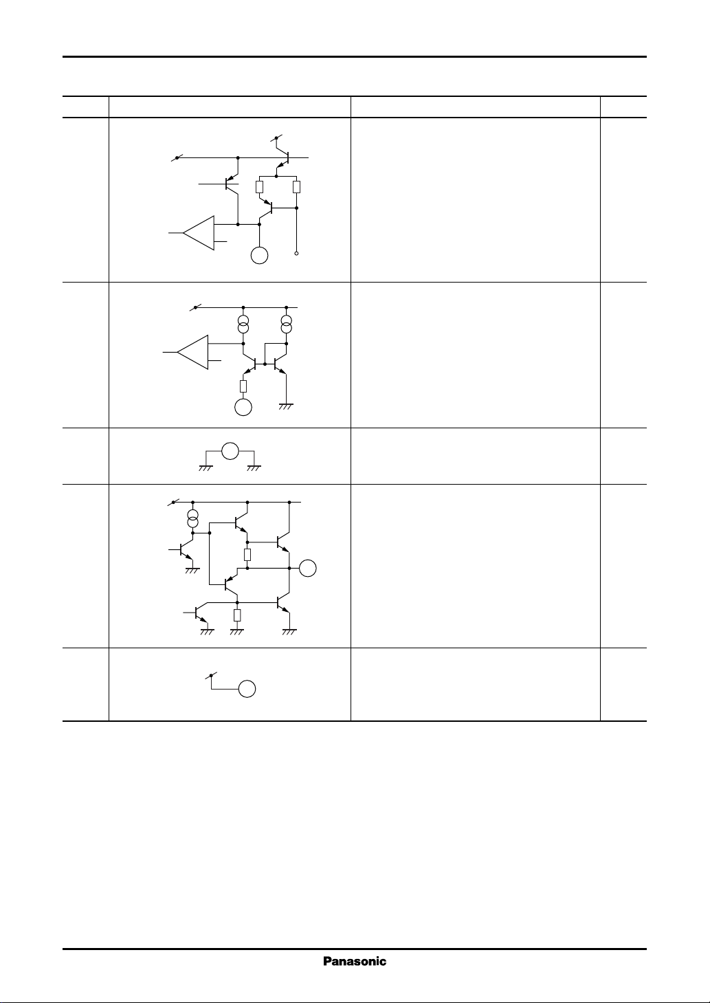
■ Terminal Equivalent Circuits
Pin No. Equivalent circuit Description I/O
1 TDL: I
2 TOFF:
V
REF
Transformer reset detection terminal.
When the transformer reset is detected and low
1
High-
side
clamp
Low-
side
clamp
is inputted into the terminal, the output of the IC
(V
) becomes high. However, low-level sig-
OUT
nal under the minimum off-period determined
by the T
is ignored.
OFF
Terminal for connecting the resistor and capaci-
V
CC
tor for determining the minimum off-period (low)
of the IC output (V
OUT
).
An equation for approximate calculation of the
Comp.
0.1 V
2
minimum off-period (T
T
= 2.2 × C × R
OFF
) is as follows:
OFF
C: External capacitance
R: External resistance
3
AN8028 Voltage Regulators
■ Terminal Equivalent Circuits (continued)
Pin No. Equivalent circuit Description I/O
3 TON:
V
REF
Comp.
0.7 V
V
CC
Terminal for connecting the capacitor for determining the maximum on-period (high) of the IC
output (V
). An equation for approximate
OUT
calculation of the maximum on-period (TON) is
as follows:
T
= 6 500 × C
3
FB
ON
C: External capacitance
4 CLM: I
V
REF
Input terminal for detection of the pulse-bypulse overcurrent protection.
Comp.
Normally, it is recommended that a filter be
attached externally.
(−)
4
5 GND:
5
6V
V
CC
Grounding terminal.
:O
OUT
Output terminal for directly driving the power
MOSFET.
It uses the totem pole type output.
6
The maximum rating of the output current:
Peak: ±1 A
DC: ±150 mA
7V
:
CC
Terminal for applying power supply voltage.
7
It monitors the supply voltage and has the operation threshold of start/stop/OVP reset.
4
 Loading...