

Panasonic AN8026 Datasheet
Voltage Regulators
AN8026
Self-excited RCC pseudo-resonance type
AC-DC switching power supply control IC
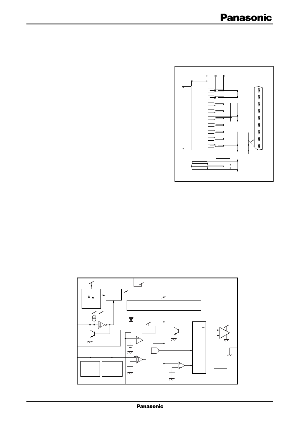
23.3±0.3
2.4±0.25
6.0±0.3
9
8
7
6
5
4
3
2
1
0.3
SIP009-P-0000C
■ Overview
The AN8026 is an IC developed for controlling the
self-excited switching power supply employing the RCC
pseudo-resonance type control method.
It is compact, equipped only with the necessary minimum functions.
The maximum on-period and the minimum off-period can be set separately by using the external capacitor
and resistor respectively.
It is suitable for the power supply of AV equipment.
■ Features
• Operating supply voltage range:
Stop voltage (8.6 V typical) to 34 V
• Output block employs the totem pole system.
• Power MOSFET can be directly driven.
(output peak current: ±1 A maximum)
• Small pre-start operating current (80 µA typical) allows using a small size start resistor.
• Built-in pulse-by-pulse overcurrent protection function
• Incorporating protection circuit against malfunction at low voltage (start/stop: 14.9 V/8.6 V)
• Built-in overvoltage protection function (externally resettable)
• Equipped with frequency (VF) control function.
• 9-pin single inline package expands the freedom of board design.
+0.1
–0.05
3.3±0.25
0.5±0.1
2.54
1.5±0.25
1.5±0.25
3.0±0.3
Unit: mm
30°
1.4±0.3
■ Applications
• Televisions, facsimiles, printers, scanners, video equipment
■ Block Diagram
OVP
FB
TDL
U.V.L.O.
8.6V1.5
8
9
1
Low-side
clamp
0 V
Signal
V
V
REF
(7.1 V)
High-side
clamp
2.8 V
2
TOFF
CC
V
7
Switch
diode
0.1 V
0.7 V
I
FB
Current source
3
TON
0.7 V
Q
RS
latch
R
S
Q
CLM
6
IN
IN
V
OUT
5
GND
4
CLM
1
AN8026 Voltage Regulators
■ Pin Descriptions
Pin No. Symbol Description
1 TDL Transformer reset detection
2 TOFF Pin for connecting C and R to set minimum off-period
3 TON Pin for connecting C to set minimum on-period
4 CLM Input pin for overcurrent protection detection
5 GND Grounding pin
6V
OUT
7VCCPower supply voltage pin
8 OVP Input pin for overvoltage protection circuit
9 FB Photocoupler connection pin for error voltage feedback
■ Absolute Maximum Ratings
Parameter Symbol Rating Unit
Supply voltage V
Peak output current I
Power dissipation P
Operating ambient temperature
Storage temperature
Note)*: Expect for the operating ambient temperature and storage temperature, all ratings are for Ta = 25°C.
*
Output pin
*
CC
6PEAK
D
T
opr
T
stg
35 V
±1A
874 mW
−30 to +85 °C
−55 to +150 °C
■ Recommended Operating Range
Parameter Symbol Range Unit
Supply voltage V
CC
■ Electrical Characteristics at VCC = 18 V, Ta = 25°C
Parameter Symbol Conditions Min Typ Max Unit
U.V.L.O. start supply voltage V
U.V.L.O. operation stop supply voltage V
U.V.L.O. start-to-stop supply voltage ∆V
OVP operation threshold voltage V
OVP operation threshold current I
OVP release voltage V
OVP operating circuit current 1 I
OVP operating circuit current 2 I
TDL threshold voltage V
TDL upper limit clamp voltage V
TDL lower limit clamp voltage V
CLM threshold voltage V
7START
7STOP
7
8OVP
8OVP
7OVP
7OVP1VCC
7OVP2VCC
1TDL
1TDL/H ITDL
1TDL/L ITDL
4CLM
= 10 V, V
= 20 V, V
= 3mA 2 2.8 3.6 V
= −3mA − 0.3 0 0.3 V
From stop voltage to 34 V
13.4 14.9 16.4 V
7.7 8.6 9.5 V
5.7 6.3 6.9 V
6.7 7.9 9.1 V
0.5 0.75 1 mA
7.4 8.2 9 V
= 9.1 V 0.66 0.89 1.12 mA
OVP
= 9.1 V 3.5 4.7 5.9 mA
OVP
0.5 0.7 0.9 V
0.7 0.75 0.8 V
2
Voltage Regulators AN8026
■ Electrical Characteristics at VCC = 18 V, Ta = 25°C (continued)
Parameter Symbol Conditions Min Typ Max Unit
TON maximum on-period current I
TON upper limit voltage V
TON lower limit voltage V
TOFF upper limit voltage V
TOFF lower limit voltage V
Output oscillation frequency f
Output current feedback current gain G
Pre-start low-level output voltage V
Low-level output voltage 1 V
Low-level output voltage 2 V
High-level output voltage 1 V
High-level output voltage 2 V
Pre-start circuit current I
Circuit current 1 I
Circuit current 2 I
7OPR(1)VCC
7OPR(2)VCC
TDL flowing-out current I
3TON/H
3TON/L
2TOFF/H
2TOFF/L
FB terminal = open −125 −100 −75 µA
3TON
TON terminal = GND
FB terminal = open 0.55 0.7 0.8 V
FB terminal = open − 0.1 0.05 0.2 V
0.7 0.9 1.1 V
− 0.1 0.05 0.2 V
CON = 2 200 pF, R
OSC
C
OFF
IFBIFB
6STB/LVCC
6L(1)IOUT
6L(2)IOUT
6H(1)IOUT
6H(2)IOUT
7STBVCC
= 1 000 pF
= −1 mA 5.25 7 8.75
= 10 V, I
= 10 mA 0.9 2 V
= 100 mA 1.1 2.2 V
= −10 mA 15.7 16.5 V
= −100 mA 15.5 16.3 V
= 12 V 40 80 120 µA
= 1.5 kΩ 50 60 70 kHz
OFF
= 10 mA 1 1.25 V
OUT
= 18 V 7.4 9.5 11.6 mA
TON terminal = GND
FB terminal = open
= 34 V 7.8 10 12.2 mA
TON terminal = GND
FB terminal = open
V
1TDL
= 0.3 V −28 −20 µA
TDL
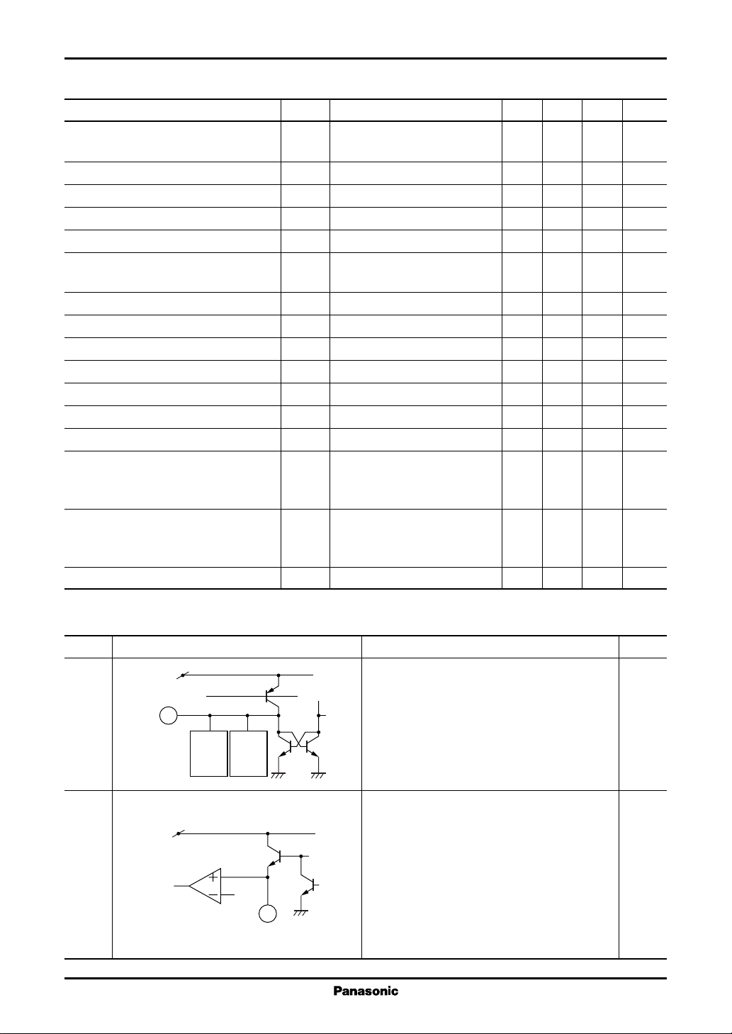
■ Terminal Equivalent Circuits
Pin No. Equivalent circuit Description I/O
1 TDL: I
2 TOFF:
V
REF
1
High-
Low-
side
clamp
side
clamp
Transformer reset detection terminal.
When the transformer reset is detected and low is
inputted into the terminal, the output of the IC
(V
) becomes high. However, low-level sig-
OUT
nal under the minimum off-period determined
by the T
is ignored.
OFF
Terminal for connecting the resistor and capaci-
V
CC
tor for determining the minimum off-period (low)
of the IC output (V
OUT
).
An equation for approximate calculation of the
Comp.
0.1 V
2
minimum off-period (T
T
= 2.2 × C × R
OFF
) is as follows:
OFF
C: external capacitance
R: external resistance
3
AN8026 Voltage Regulators
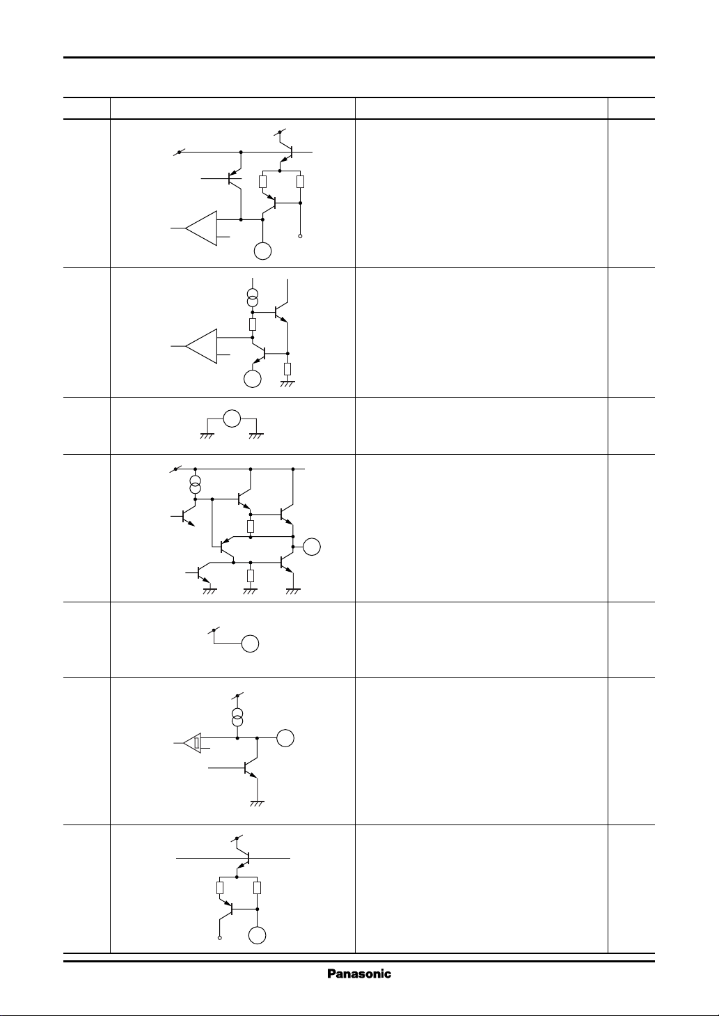
■ Terminal Equivalent Circuits (continued)
Pin No. Equivalent circuit Description I/O
3 TON:
V
REF
Comp.
0.7 V
4 CLM: I
Comp.
(+)
V
CC
Terminal for connecting the capacitor for determining the maximum on-period (high) of the IC
output (V
). An equation for approximate
OUT
calculation of the maximum on-period (TON) is
as follows:
FB
3
T
= 6 500 × C
ON
C: External capacitance
Input terminal for detection of the pulse-bypulse overcurrent protection.
Normally, it is recommended that a filter be
attached externally.
4
5 GND:
5
6V
V
CC
Grounding terminal.
:O
OUT
Output terminal for directly driving the power
MOSFET.
It uses the totem pole type output.
6
The maximum rating of the output current:
Peak: ±1 A
DC: ±150 mA
7V
:
CC
Terminal for applying power supply voltage.
7
It monitors the supply voltage and has the operation threshold of start/stop/OVP reset.
8 OVP: I
When overvoltage of the power supply output is
detected and high is inputted to the terminal, it
8
Comp.
turns off the internal circuit. At the same time, it
holds that condition (latch).
To reset the OVP latch, the terminal voltage should
be decreased to low, or the VCC should be decreased
to a voltage lower than the release voltage.
9 FB: I
V
CC
Terminal for connecting the photocoupler for
error voltage feedback of the power supply output.
It is possible to cancel about 150 µA of the dark
TON
9
current of photocoupler.
4
 Loading...