

Panasonic AN8021SB, AN8021L Datasheet
Voltage Regulators
21.7
±0.3
9
8
7
6
5
4
3
2
1
4.3
±0.3
1.0
±0.25
2.7
±0.25
1.4
±0.25
1.35
±0.25
0.4
±0.25
0.5
±0.1
1.2
±0.25
2.54
0.3
+0.1
–0.05
AN8021L, AN8021SB
AC-DC switching power supply control IC
■ Overview
The AN8021L and AN8021SB are ICs which are
suitable for controlling the switching power supply using primary side control method.
Those are most suited for a switching power supply
of relatively small capacity. Less frequently used functions are removed and only the necessary minimum functions are incorporated, so that they are compact and very
easy to use.
Moreover, the internal settings are incorporated as
much as possible, thus cost down can be realized by decreasing the peripheral parts.
■ Features
• It operates at a control frequency up to 700 kHz, realiz-
ing the output rise time of 35 ns and the output fall time
of 25 ns.
• Pre-start operating current is as small as 70 µA (typical)
so that it is possible to use a miniaturized start resistor.
• Output block employs totem pole method.
The absolute maximum rating of ±1.0 A (peak) allows
the direct drive of power MOSFET.
• Built-in pulse-by-pulse overcurrent protection circuit
• Built-in protection circuit against malfunction at low
voltage (on/off: 14.2 V/9.2 V)
• Equipped with timer latch function and overvoltage protection circuit.
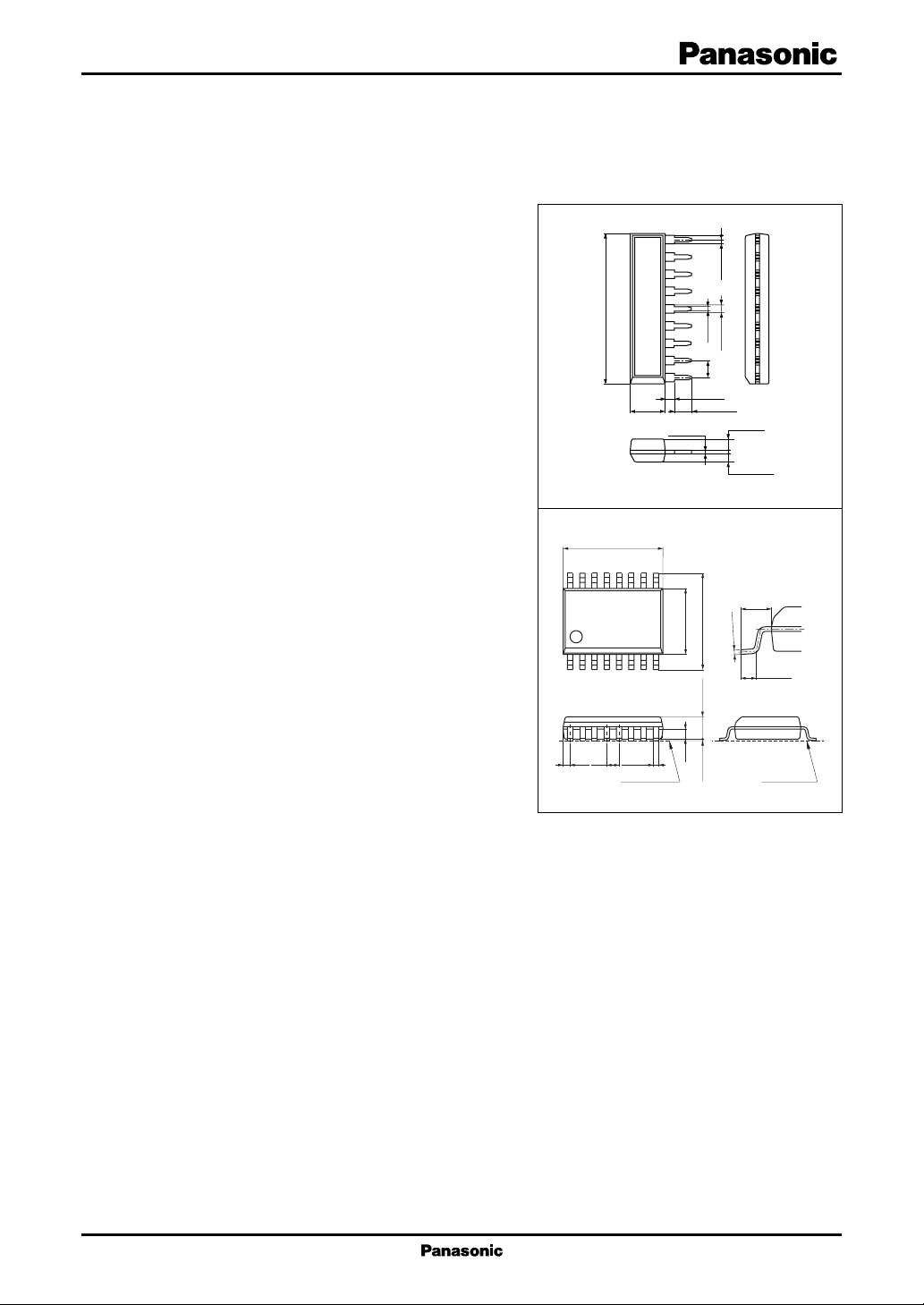
• Two kinds of packages: 9-pin SIP, 16-pin SOP
AN8021L Unit: mm
SIP009-P-0000D
AN8021SB Unit: mm
6.50
±0.30
16
1
(0.45)
0.80
9
±0.30
±0.30
6.30
4.30
8
±0.20
1.50
±0.10
0.65
±0.10
0.10
0.35
Seating plane
SSOP016-P-0225B
+0.10
1.00
-0.05
0.15
±0.20
0.50
±0.05
Seatng plane
■ Applications
• Various power supply equipment
1
AN8021L, AN8021SB Voltage Regulators
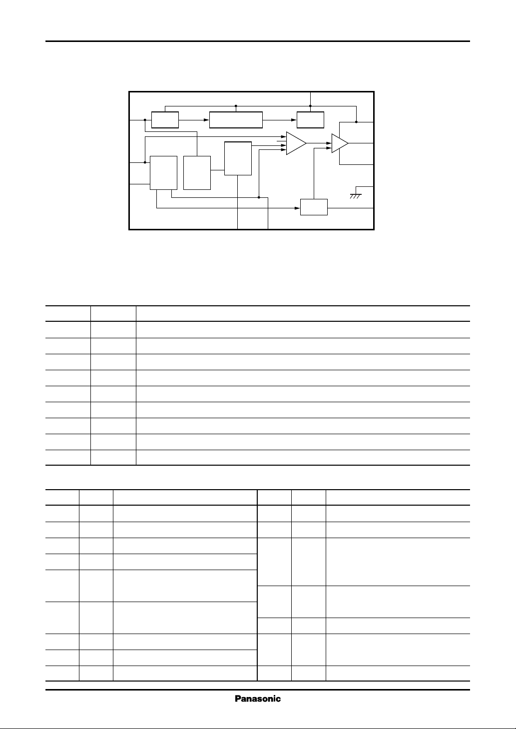
■ Block Diagram
CC
(4)SV
TIM/OVP
8
OVP
Start/Stop
(5)
4.1 V
CT
(13)
RT
3
2
OSC OCL
FB
(12)
9
(6)
IFB
Note) The number in ( ) shows the pin number for the AN8021SB.
1
Reset
SS
(11)
PWM
V
REF
CLM
Drive
7
V
CC
(3)PV
6
V
OUT
(2)
5
GND
(1)PGND
(16)SGND
4
CLM(−)
(15)
CC
■ Pin Descriptions
• AN8021L
Pin No. Symbol Description
1 SS Soft start pin
2 RT Resistor connection pin that determines charge and discharge current of triangular wave
3 CT Triangular wave generating capacitor connection pin
4 CLM(−) Pulse-by-pulse overcurrent protection input pin
5 GND Grounding pin
6V
OUT
7VCCPower supply voltage pin
8 TIM/OVP Pin for overvoltage protection and timer latch (joint use)
9 IFB Current feedback signal input pin from power-supply-output photocoupler
Power MOSFET direct drive pin
• AN8021SB
Pin No. Symbol Description
1 PGND Grounding pin
2V
Power MOSFET direct drive pin
OUT
3PVCCPower supply voltage pin
4SVCCPower supply voltage pin
5
TIM/OVP
Pin for overvoltage protection and
timer latch combined use
6 IFB Power supply output photocoupler
current feedback signal input pin
7 N.C. N.C.
8 N.C. N.C.
9 N.C. N.C.
2
Pin No. Symbol Description
10 N.C. N.C.
11 SS Soft start pin
12 RT Charge and discharge current of
triangular wave determining resistance
connection pin
13 CT Triangular wave generating capacitor
connection pin
14 N.C. N.C.
15 CLM(−) Pulse-by-pulse overcurrent protection
input pin
16 SGND Grounding pin
Voltage Regulators AN8021L, AN8021SB
■ Absolute Maximum Ratings
Parameter Symbol Rating Unit
Supply voltage V
OVP terminal allowable application voltage V
CLM terminal allowable application voltage V
SS terminal allowable application voltage V
Constant output current I
Peak output current I
IFB terminal allowable application voltage I
Power dissipation AN8021L P
CC
OVP
CLM
SS
O
OP
FB
D
AN8021SB 340
Operating ambient temperature
Storage temperature
Note)*: Expect for the operating ambient temperature and storage temperature, all ratings are for Ta = 25°C.
*
*
T
opr
T
stg
■ Recommended Operating Range
Parameter Symbol Range Unit
Timing resistor R
T
R
7
35 V
V
CC
V
− 0.3 to +7.0 V
− 0.3 to +7.0 V
±150 mA
±1 000 mA
−5mA
658 mW
−30 to +85 °C
−55 to +150 °C
15 to 20 kΩ
■ Electrical Characteristics at Ta = 25°C
Parameter Symbol Conditions Min Typ Max Unit
Start voltage V
Stop voltage V
Standby bias current I
Operating bias current I
OVP operating bias current 1 I
OVP operating bias current 2 I
OVP operating threshold voltage V
OVP release supply voltage V
Timer latch charge current I
Timer latch start feedback current I
Soft-start charge current I
Overcurrent protection threshold voltage 1
Pre-start low-level output voltage V
Low-level output voltage V
High-level output voltage V
Oscillation frequency 1 f
Maximum duty 1 Du
Feedback current at 0% duty I
Feedback current at maximum duty I
CC-START
CC-STOP
CC-STB
CC-OPR
CC-OVP1VCC
CC-OVP2VCC
TH-OVPVCC
CC-OVPC
CH-TIM
FB-TIM
CH-SS
V
TH-CLM1VCC
OL-STBVCC
OL
OH
OSC1
max1
FB-Du
FB-Du
13.0 14.2 15.4 V
8.5 9.2 9.9 V
VCC = 12 V 50 70 105 µA
VCC = 34 V 6.4 8.0 9.6 mA
= 20 V 2.4 3.0 3.6 mA
= 10 V 0.44 0.55 0.66 mA
= 18 V 5.4 6.0 6.6 V
7.6 8.4 9.2 V
VCC = 18 V, RT = 19 kΩ−20 −30 −40 µA
VCC = 18 V − 0.37 − 0.5 − 0.63 mA
VCC = 18 V, RT = 19 kΩ−20 −30 −40 µA
= 18 V −180 −200 −220 mV
= 12 V, IO = 10 mA 0.8 1.8 V
VCC = 18 V, IO = 100 mA 1.3 1.8 V
VCC = 18 V, IO = −100 mA 15.0 16.5 V
VCC = 18 V 175 200 225 kHz
VCC = 18 V 62 66 70 %
VCC = 18 V −1.1 −1.5 −1.9 mA
min
VCC = 18 V − 0.37 − 0.5 − 0.63 mA
max
3
AN8021L, AN8021SB Voltage Regulators
■ Electrical Characteristics at Ta = 25°C (continued)
• Design reference data
Note) The characteristics listed below are theoretical values based on the IC design and are not guaranteed.
Parameter Symbol Conditions Min Typ Max Unit
Oscillation frequency 2 f
Overcurrent protection delay time t
OSC2
Dry-CLMVCC
Output voltage rise time t
Output voltage fall time t
■ Terminal Equivalent Circuits
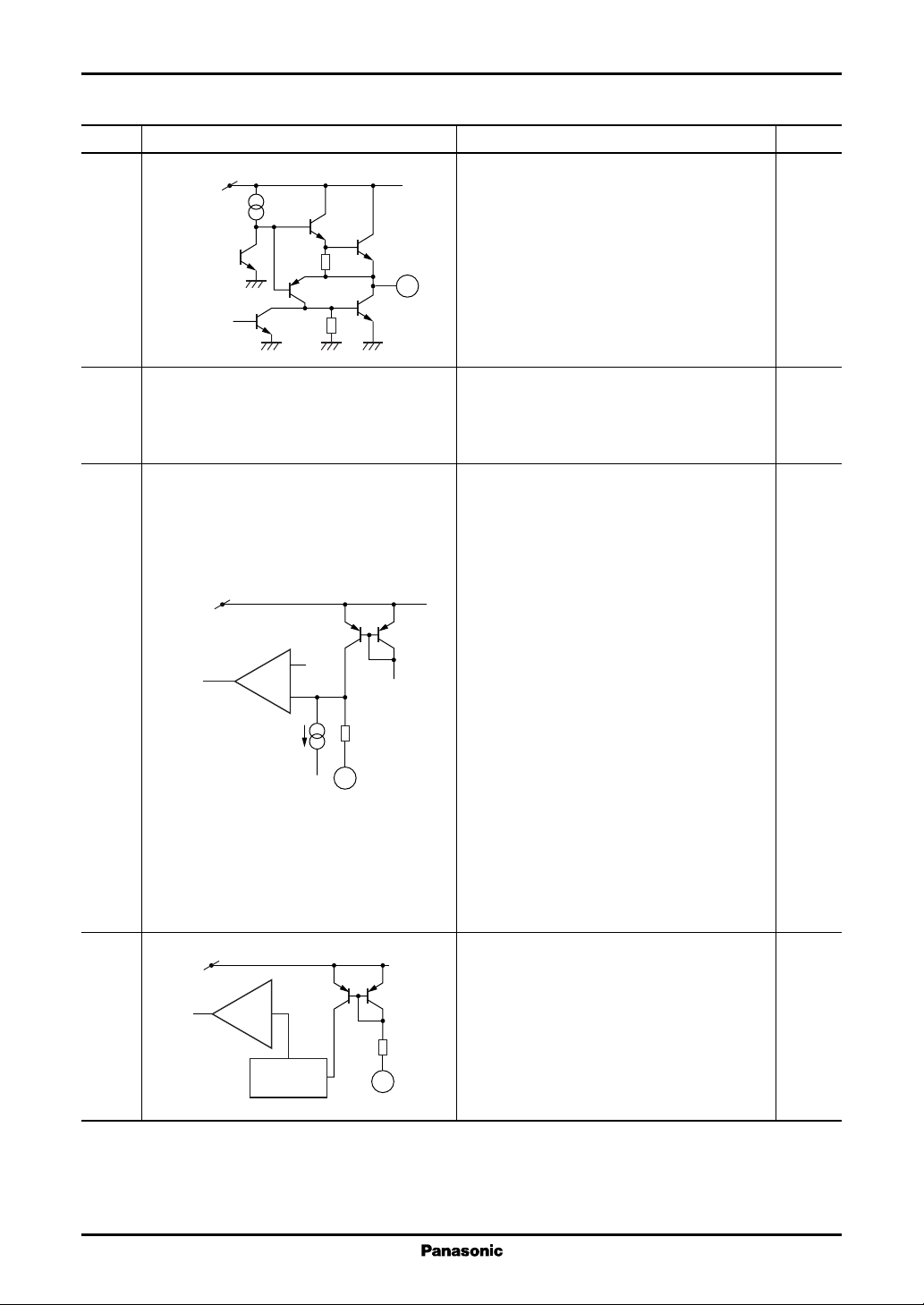
Pin No. Equivalent circuit Description I/O
1 SS:
(11) Soft start terminal.
500 Ω
1
(11)
PWM
comp.
Ta = −30°C to +85°C 160 240 kHz
= 18 V under no load 200 ns
VCC = 18 V under no load 35 ns
r
VCC = 18 V under no load 25 ns
f
When V
is applied, the capacitor connected to
CC
this pin is charged, and the output duty is decreased by inputting the capacitor voltage to the
PWM.
2 RT:
(12) The terminal for connecting a resistor to deter-
V
REF
mine the charge and discharge current of the
triangular wave.
500 Ω
2
(12)
3 CT:
(13) The terminal for connecting a capacitor to gen-
V
REF
(13)
I
O
erate the triangular wave.
3
2I
O
4 CLM(−): I
(15) The input terminal for pulse-by-pulse
V
REF
Reset
PWM
comp.
overcurrent protection. It is usually required to
attach an external filter.
4
(15)
5 GND, (PGND), (SGND):
(1)(16) Grounding terminal.
Note) The number in ( ) shows the pin number for the AN8021SB.
4
Voltage Regulators AN8021L, AN8021SB
■ Terminal Equivalent Circuits (continued)
Pin No. Equivalent circuit Description I/O
6V
PV
(2) The terminal for directly driving a power
CC
6
(2)
7 VCC , (PVCC), (SVCC):
(3)(4) Supply voltage terminal.
8 TIM/OVP: I
(5) The terminal with double functions such as OVP
SV
CC
6 V
Comp.
5 µA
500 Ω
8
(5)
9 IFB : I
V
(6) The terminal into which the current feedback
REF
PWM
comp.
500 Ω
I/V
conversion
9
(6)
:O
OUT
MOSFET.
It monitors the supply voltage and has operating threshold value for start/stop/OVP reset.
(overcurrent protection) and timer latch terminal.
[OVP]
When it receives the overvoltage signal of the
power supply output and high is input to the
terminal, internal circuit is turned off. At the
same time, this condition (latch) is hold. To reset the OVP latch, it is necessary to reduce V
CC
under the release voltage.
[Timer latch]
The output voltage drop due to the overcurrent
condition of power supply output is detected
through the current level for IFB-input. When
I
becomes less than current of a certain value,
IFB
charge current flows into the capacitor connected to this terminal. When the capacitor is
charged to the threshold voltage of OVP, OVP
starts to operate and the IC stays stop.
signal is input from the photocoupler of the
power supply output.
Note) The number in ( ) shows the pin number for the AN8021SB.
5
 Loading...