

Voltage Regulators
AN8021NS
External excitation flyback AC-DC switching power supply control IC
■ Overview
The AN8021S is a switching power supply control IC
that controls the power supply from the primary side. It is
optimal for relatively small switching power supplies. All
rarely used functions have been removed from the
AN8021S and as a result it is an extremely easy-to-use
compact device. Furthermore, internal settings are
implemented as many as we can, cost cut is possible with
reduced external parts.
■ Features
•
Supports operation at switching frequencies up to
700 kHz and achieves a 35 ns output rise time and a 25
ns output fall time.
•
Extremely low pre-startup current consumption of 70
µA (typical) allows a significantly smaller startup resistor
to be used.
•
Totem pole circuit structure adopted in the output block.
•
Output current absolute maximum rating of ±1.0 A
(peak) for direct driving of power MOSFET.
•
Pulse-by-pulse overcurrent protection circuit
•
Low voltage malfunction prevention circuit
On/off: 14.2 V/9.2 V
•
Timer latch and overvoltage protection functions
•
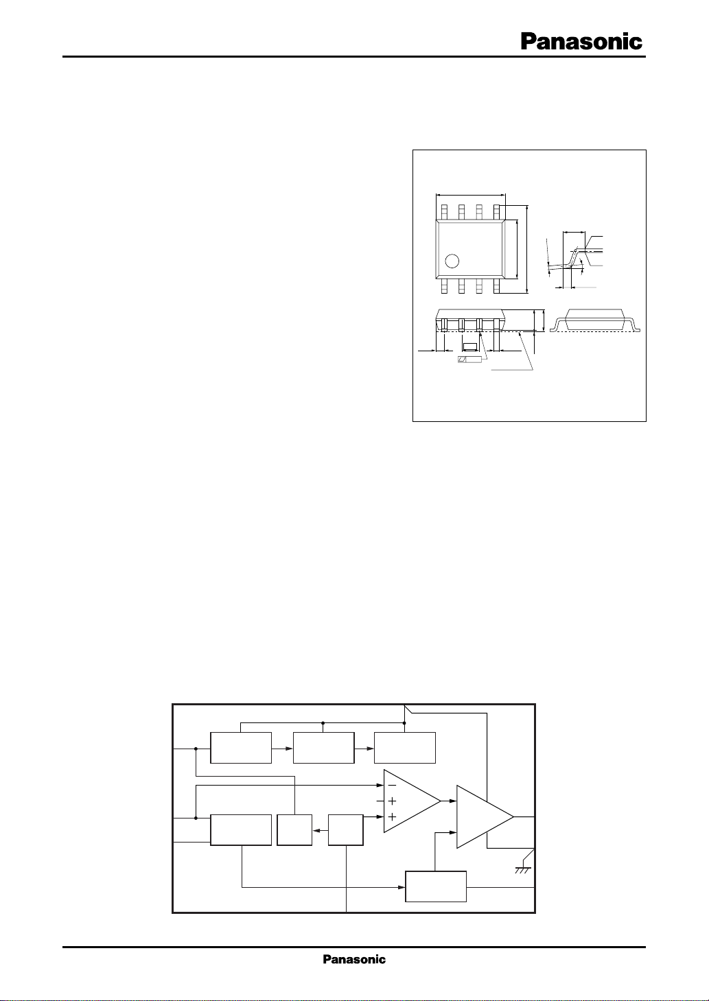
Package: SONF-8D
5.01
±0.20
8
14
(0.60)
1.27
0.10
Seating plane
SOP008-P-0225C
Unit: mm
5
(1.05)
±0.20
±0.20
–0.05
+0.10
4.30
6.40
0.15
0° to 10°
0.50
±0.20
max.
±0.10
1.75
1.45
±0.10
+0.10
0.40
–0.05
0.10
■ Applications
• Switching power supplies
■ Block Diagram
CT
RT
3
6
5
TIM/OVP
OVP Start/Stop
OSC
OCL FB
CC
V
2
V
REF
Reset
PWM4.2 V
Drive
CLM
1
V
OUT
8
GND
7
CLM
4
IFB
1

AN8021NS Voltage Regulators
■ Pin Descriptions
Pin No. Symbol Description
1V
2V
OUT
CC
3 TIM/OVP OVP (overvoltage protection) and timer latch functions.
4 IFB Input for the current feedback signal provided from a photocoupler of the power supply
5 RT Connection for the resistor that determines the charge and discharge currents of the triangular
6 CT Connection for the capacitor used to generate the triangular wave.
7 CLM Pulse-by-pulse overcurrent protection input. Normally, an external filter is required.
8 GND Ground
Direct power MOSFET drive output
Power supply. This pin monitored, and has threshold voltages for startup, stop, OVP reset,
and other functions.
OVP:
Accepts a power supply overvoltage detection signal. When a high-level signal is input,
internal circuits are turned off and this state is latched. To reset this OVP latched state,
the V
voltage should be lowered to below the release voltage.
CC
Timer latch:
The IC detects output voltage drops due to overcurrent states in the power supply output by
monitoring the magnitude of the current input to the IFB pin. In particular, when the current
I
has fallen below a certain level, a charge current flows into the capacitor connected to
IFB
this pin externally. When that capacitor is charged to the OVP threshold voltage, OVP
operates and the IC keeps a stopped state.
output.
wave. In this device, the charge and discharge currents are the same.
■ Absolute Maximum Ratings
Parameter Symbol Rating Unit
Supply voltage V
OVP pin allowable application voltage V
CLM pin allowable application voltage V
Supply current I
Steady-state output current I
Peak output current I
CC
OVP
CLM
CC
O
OP
IFB pin allowable application current IFB −5mA
Power dissipation
Operating temperature
Storage temperature
Notes) 1. *1: Items other than the storage temperature and operating temperature are all stipulated for an ambient temperature T
2. Currents or voltages may not be applied to any pins not stipulated above. For circuit currents, a positive (+) value
*2
*1
*1
= 25°C.
*2: Applies when Ta = 85°C for the independent IC without a heat sink.
indicates current flowing into the IC, and a negative (−) value indicates current flowing out of the IC.
P
D
T
opr
T
stg
2
35 V
V
CC
− 0.3 to +7.0 V
mA
+150 mA
±1 000 mA
122 mW
−30 to +85 °C
−55 to +150 °C
V
a
 Loading...