

Panasonic AN8018SA Datasheet
Voltage Regulators
AN8018SA
1.8-volt 2-channel step-up, step-down,
or inverting DC-DC converter control IC
■ Overview
The AN8018SA is a two-channel PWM DC-DC con-
verter control IC that features low-voltage operation.
This IC can obtain the step-up, step-down and invert-
ing voltages with a small number of external components.
The minimum operating voltage is as low as 1.8 V so
that it can operate with two dry batteries. In addition,
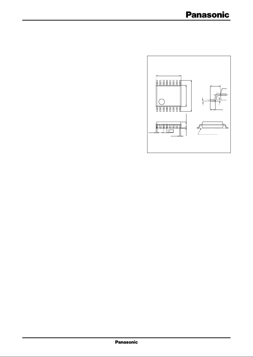
since it uses the 16-pin surface mounting type package
with 0.65 mm pitch, it is suitable for miniaturized highly
efficient potable power supply.
5.0±0.2
16
18
9
4.4±0.2
6.4±0.3
1.2±0.20.1±0.1
−0.05
+0.10
5
.1
0
Unit: mm
(1.0)
0° to 10°
0.5±0.2
■ Features
(0.225)
0.65
0.22
+0.10
− 0.05
• Wide operating supply voltage range (1.8 V to 14 V)
• Incorporating a high precision reference voltage circuit
(allowance: ± 2%)
SSOP016-P-0225A
• Control in a wide output frequency range is possible
(20 kHz to 1 MHz).
• Built-in wideband error amplifier (single gain bandwidth
10 MHz typical)
• Built-in timer latch short-circuit protection circuit
(charge current 1.1 µA typical)
• Incorporating the under-voltage lock-out circuit (U.V.L.O.)
(circuit operation-starting voltage 1.67 V typical)
• Dead-time is variable.
• Flatness of switching current can be obtained by staggering the turn-on timing of each channel.
• Built-in unlatch function
When DT1 pin is low level, or DT2 pin is high level, independent turn-off is possible.
• Incorporating a on/off control function
(active-high control input, standby mode current: 5 µA maximum)
• Parallel operation is possible.
• Output block
• Totem pole 1 output
• Output source-current: −50 mA maximum
(Constant current output with a less supply voltage fluctuation is
possible by connecting an external resistor to pin 11)
• Output sink-current: +80 mA maximum
• Open-collector 1 output
• Output current: 50 mA maximum
Seating plane
■ Applications
• LCD displays, digital still cameras, and PDAs
1
AN8018SA Voltage Regulators
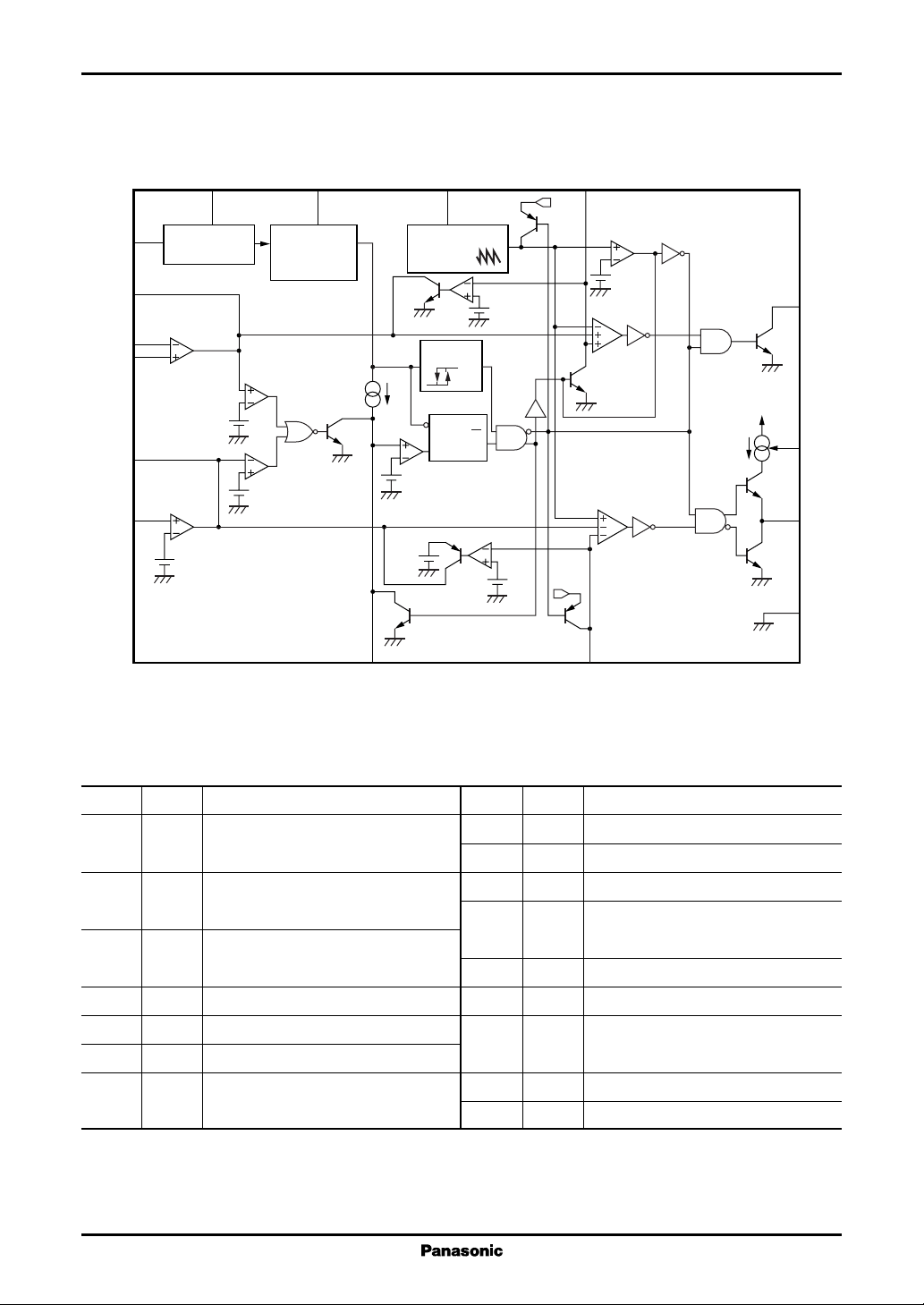
■ Block Diagram
On/
off
FB1
IN−1
IN+1
FB2
IN+2
15
On/off
control
5
Error amp. 1
4
3
0.9 V
13
Error amp. 2
14
1.19 V
CC
V
9
REF
V
16
Reference
voltage source
V
REF
1.19 V
OSC
1
Triangular wave
oscillation
0.2 V
DT1
6
V
REF
0.9 V
7
PWM1
Out1
Unlatch1
U.V.L.O.
H
L
Latch
V
CC
11
RB2
10
Out2
8
GND
0.22 V
S.C.P.
comp.
R
Q
S
V
REF
PWM2
0.9 V
0.9 V
V
REF
Unlatch2
2
12
S.C.P.
■ Pin Descriptions
Pin No. Symbol Description
1 OSC Pin for oscillation timing resistor
and capacitor connection
2 S.C.P.
3IN+1 Error amplifier 1 block noninverting
4IN−1
5 FB1 Output pin of error amplifier 1 block
6 DT1 PWM1 block dead-time setting pin
7 Out1 Out1 block open-collector type
Pin for connecting the time constant setting capacitor for short-circuit protection
input pin
Error amplifier 1 block inverting input pin
output pin
DT2
Pin No. Symbol Description
8 GND Grounding pin
9VCCPower supply voltage application pin
10 Out2 Out2 block push-pull type output pin
11 RB2 Out2 block output source current
setting resistor connection pin
12 DT2 PWM2 block dead-time setting pin
13 FB2 Output pin of error amplifier 2 block
14 IN+2 Error amplifier 2 block inverting input
pin
15 Off On/off control pin
16 V
Reference voltage output pin
REF
2
Voltage Regulators AN8018SA
■ Absolute Maximum Ratings
Parameter Symbol Rating Unit
Supply voltage V
Off terminal allowable application voltage V
IN+1 terminal allowable application voltage
IN−1 terminal allowable application voltage
IN+2 terminal allowable application voltage
Out1 terminal allowable application voltage V
Supply current I
Out1 terminal output current I
Out2 terminal source current I
Out2 terminal sink current I
1
Power dissipation
*
Operating ambient temperature T
Storage temperature T
Note) 1. Do not apply external currents or voltages to any pins not specifically mentioned.
For the circuit currents, '+' denotes current flowing into the IC, and '−' denotes current flowing out of the IC.
2. Except for the power dissipation, operating ambient temperature, and storage temperature, all ratings are for Ta = 25°C.
3.*1: Ta = 85 °C. For the independent IC without a heat sink. Note that applications must observe the derating curve for the
relationship between the IC power consumption and the ambient temperature.
2: V
, V
, V
*
IN−1
IN-1
= VCC when VCC < 6 V.
IN+2
CC
OFF
2
*
V
IN−1
2
*
V
IN−1
2
*
V
IN+2
OUT
CC
O
SO(OUT)
SI(OUT)
P
D
opr
stg
15 V
15 V
6V
6V
6V
15 V
mA
+50 mA
−50 mA
+80 mA
135 mW
−30 to +85 °C
−55 to +150 °C
■ Recommended Operating Range
Parameter Symbol Range Unit
Supply voltage V
Off control terminal application voltage V
Output source current I
Output sink current I
Timing resistance R
Timing capacitance C
Oscillation frequency f
Short-circuit protection time constant C
CC
OFF
SO(OUT)
SI(OUT)
T
T
OUT
SCP
setting capacitance
Output current setting resistance R
■ Electrical Characteristics at VCC = 2.4 V, C
B
= 0.1 µF, Ta = 25°C
REF
Parameter Symbol Conditions Min Typ Max Unit
Reference voltage block
Reference voltage V
REFIREF
= − 0.1 mA 1.166 1.19 1.214 V
Input regulation with input fluctuation Line VCC = 1.8 V to 14 V 15 30 mV
Load regulation Load I
= − 0.1 mA to −1 mA −20 −5 mV
REF
1.8 to 14 V
0 to 14 V
−40 (minimum) mA
70 (maximum) mA
1 to 51 kΩ
100 to 10 000 pF
20 to 1 000 kHz
1 000 (minimum) pF
180 to 15 000 Ω
3
AN8018SA Voltage Regulators
■ Electrical Characteristics at VCC = 2.4 V, C
Parameter Symbol Conditions Min Typ Max Unit
U.V.L.O. block
Circuit operation start voltage V
Error amplifier 1 block
Input offset voltage V
Common-mode input voltage range V
Input bias current 1 I
High-level output voltage 1 V
Low-level output voltage 1 V
Output source current 1 I
Output sink current 1 I
Error amplifier 2 block
Input threshold voltage V
Input bias current 2 I
High-level output voltage 2 V
Low-level output voltage 2 V
Output source current 2 I
Output sink current 2 I
Oscillator block
Output off threshold voltage V
Output 1 block
Oscillation frequency 1 f
Output duty ratio 1 Du
Output saturation voltage V
Output leak current I
Output 2 block
Oscillation frequency 2 f
Output duty ratio 2 Du
High-level output voltage V
Low-level output voltage V
Output source current I
Output sink current I
Pull-down resistance R
PWM1 block
Output full-off input threshold V
voltage 1
Output full-on input threshold V
voltage 1
Input current 1 I
UON
IO
ICR
B1
EH1
EL1
SO(FB)1
SI(FB)1
TH
B2
EH2
EL2
SO(FB)2
SI(FB)2
TH(OSC)
OUT1RT
1
O(SAT)IO
VCC = 14 V 1 µA
OLE
OUT2RT
2
OHIO
OLIO
SO(OUT)VO
SI(OUT)VO
O
Duty = 0% 0.28 0.30 V
T0-1
Duty = 100% 0.65 0.72 V
T100-1
V
DT1
= 0.1 µF, Ta = 25°C (continued)
REF
1.59 1.67 1.75 V
−6 +6mV
0.3 0.7 V
− 0.6 − 0.2 µA
0.83 0.93 1.03 V
0.2 V
−61 −47 −33 µA
33 47 61 µA
1.16 1.19 1.22 V
0.2 0.8 µA
0.83 0.93 1.03 V
0.2 V
−61 −47 −33 µA
33 47 61 µA
0.8 0.9 1.0 V
= 12 kΩ, CT = 330 pF 185 205 225 kHz
75 80 85 %
= 30 mA 0.5 V
= 12 kΩ, CT = 330 pF 185 205 225 kHz
72 77 82 %
= −10 mA, RB = 820 Ω 1.4 V
= 10 mA, RB = 820 Ω0.2 V
= 0.7 V, RB = 820 Ω−40 −30 −20 mA
= 0.7 V, RB = 820 Ω 20 mA
20 30 40 kΩ
= 0.4 V −1.1 − 0.5 µA
DT1
4
Voltage Regulators AN8018SA
■ Electrical Characteristics at VCC = 2.4 V, C
Parameter Symbol Conditions Min Typ Max Unit
PWM2 block
Output full-off input threshold V
voltage 2
Output full-on input threshold V
voltage 2
Input current 2 I
Unlatch circuit 1 block
Input threshold voltage 1 V
Unlatch circuit 2 block
Input threshold voltage 2 V
Short-circuit protection circuit block
Input standby voltage V
Input threshold voltage 1 V
Input threshold voltage 2 V
Input latch voltage V
Charge current I
On/off control block
Input threshold voltage V
ON(TH)
Whole device
Output off consumption current I
Latch mode consumption current I
Standby current I
CC(OFF)RB
CC(LA)RB
CC(SB)
Duty = 0% 0.65 0.72 V
T0-2
Duty = 100% 0.28 0.30 V
T100-2
V
DT2
THUL1
THUL2
STBY
THPC1
THPC2
CHG
DT2
IN
V
SCP
= 0.1 µF, Ta = 25°C (continued)
REF
= 0 V −1.1 − 0.5 µA
0.15 0.20 0.25 V
0.8 0.9 1.0 V
60 120 mV
0.8 0.9 1.0 V
0.17 0.22 0.27 V
60 120 mV
= 0 V −1.43 −1.1 − 0.77 µA
0.8 1.0 1.3 V
= 820 Ω, duty = 0% 5.7 8.0 mA
= 820 Ω5.6 7.8 mA
1 µA
•
Design reference data
Note) The characteristics listed below are theoretical values based on the IC design and are not guaranteed.
Parameter Symbol Conditions Min Typ Max Unit
Reference voltage block
V
temperature characteristics V
REF
Over-current protection drive current I
REFdTTa
OC
= −30°C to +85°C −1 +1%
−11 mA
U.V.L.O. block
Reset voltage V
R
0.8 V
Error amplifier 1/2 blocks
VTH temperature characteristics V
Open-loop gain A
Single gain bandwidth f
THdTTa
V
BW
= −30°C to +85°C − 0.3 + 0.3 mV/°C
57 dB
10 MHz
Output 1/2 blocks
Frequency supply voltage f
dV
−1 +1%
characteristics
Frequency temperature characteristics f
dT
−3 +3%
5
AN8018SA Voltage Regulators
■ Electrical Characteristics at VCC = 2.4 V, C
•
Design reference data (continued)
Note) The characteristics listed below are theoretical values based on the IC design and are not guaranteed.
= 0.1 µF, Ta = 25°C (continued)
REF
Parameter Symbol Conditions Min Typ Max Unit
Output 2 block
RB terminal voltage V
B
0.36 V
Short-circuit protection block
Comparator threshold voltage V
THL
1.19 V
On/off control block
Off terminal current I
OFF
23 µA
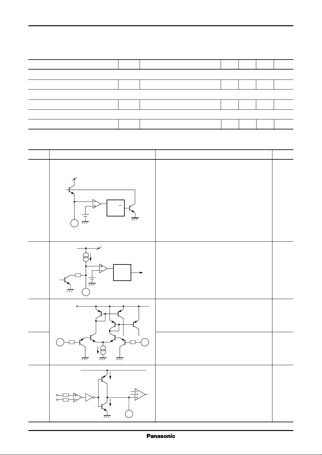
■ Terminal Equivalent Circuits
Pin No. Equivalent circuit Description I/O
1 OSC: O
V
CC
Latch
S
Q
R
0.2 V
1
2 S.C.P.: O
2 kΩ
V
1.1 µA
1.19 V
CC
Latch
S
R
Q
Output
cut-off
2
The terminal used for connecting a timing capacitor/resistor to set oscillation frequency.
Use a capacitance value within the range of 100 pF
to 10 000 pF and a resistance value within the range
of 3 kΩ to 30 kΩ. Use an oscillation frequency in the
range of 20 kHz to 1 MHz. When operating the
circuit in parallel and synchronously, the channel 2
output stops when this pin becomes 0.9 V or more.
(Refer to the "Application Notes, [7]" section.)
The terminal for connecting a capacitor to set the
time constant of the timer latch short-circuit protection circuit. Use a capacitance value in the range
of 1 000 pF or more. The charge current I
CHG
is
1.1 µA typical.
3IN+1: I
V
CC
The noninverting input pin for error amplifier 1
block.
4IN−1: I
4 3
100 Ω 100 Ω
The inverting input pin for error amplifier 1 block.
5 FB1: O
IN+1
IN−1
47 µA
OSC PWM
47 µA
5
The output pin for error amplifier 1 block.
The source current is −47 µA and the sink current
is 47 µA.
Correct the frequency characteristics of the gain
and the phase by connecting a resistor and a capacitor between this terminal and GND.
6
Voltage Regulators AN8018SA
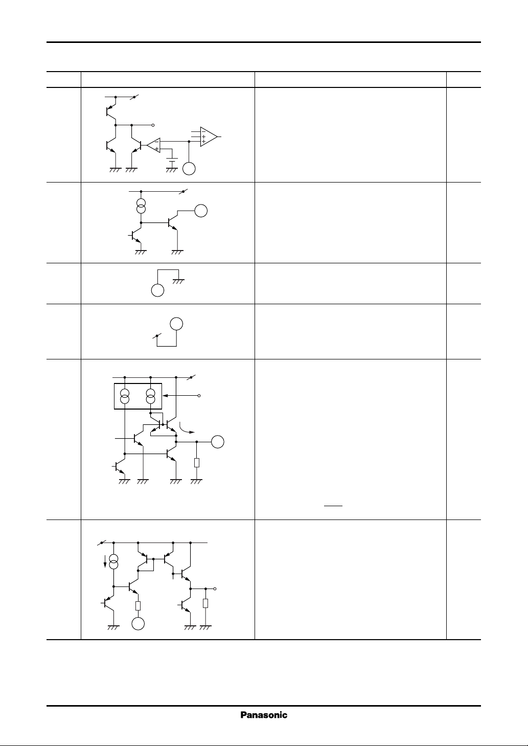
■ Terminal Equivalent Circuits (continued)
Pin No. Equivalent circuit Description I/O
6 DT1: I
7 Out1: O
8 GND:
V
0.2 V
CC
FB1
8
OSC PWM
6
V
CC
7
The pin for setting channel 1 output maximum
duty ratio.
If this terminal is set at a voltage of 0.20 V or less,
FB1 terminal becomes low-level voltage and the
protective function for channel 1 output shortcircuit will stop (Unlatch function).
The pin is open-collector type output terminal.
The absolute maximum rating of output current is
+50 mA.
Grounding terminal
9V
9
:
CC
The supply voltage application terminal
Use the operating supply voltage in the range of
1.8 V to 14 V.
10 Out2: O
V
CC
RB2
The pin is push-pull type output terminal.
The absolute maximum rating of output source
current is −50 mA.
I
SO(OUT)
30 kΩ
10
The absolute maximum rating of output sink current is +80 mA.
A constant current output with less fluctuation
with power supply voltage and dispersion can be
obtained by the resistor externally attached to RB2
pin.
V
I
11 RB2: I
V
CC
The pin for connecting a resistor for setting chan-
SO(OUT)2
= 68 ×
RB2
[A]
R
B2
nel 2 output current.
Use a resistance value in the range of 180 Ω to 1.1
kΩ.
Out2
The terminal voltage is 0.36 V (at R
= 820 Ω).
B2
120 Ω
11
7
AN8018SA Voltage Regulators
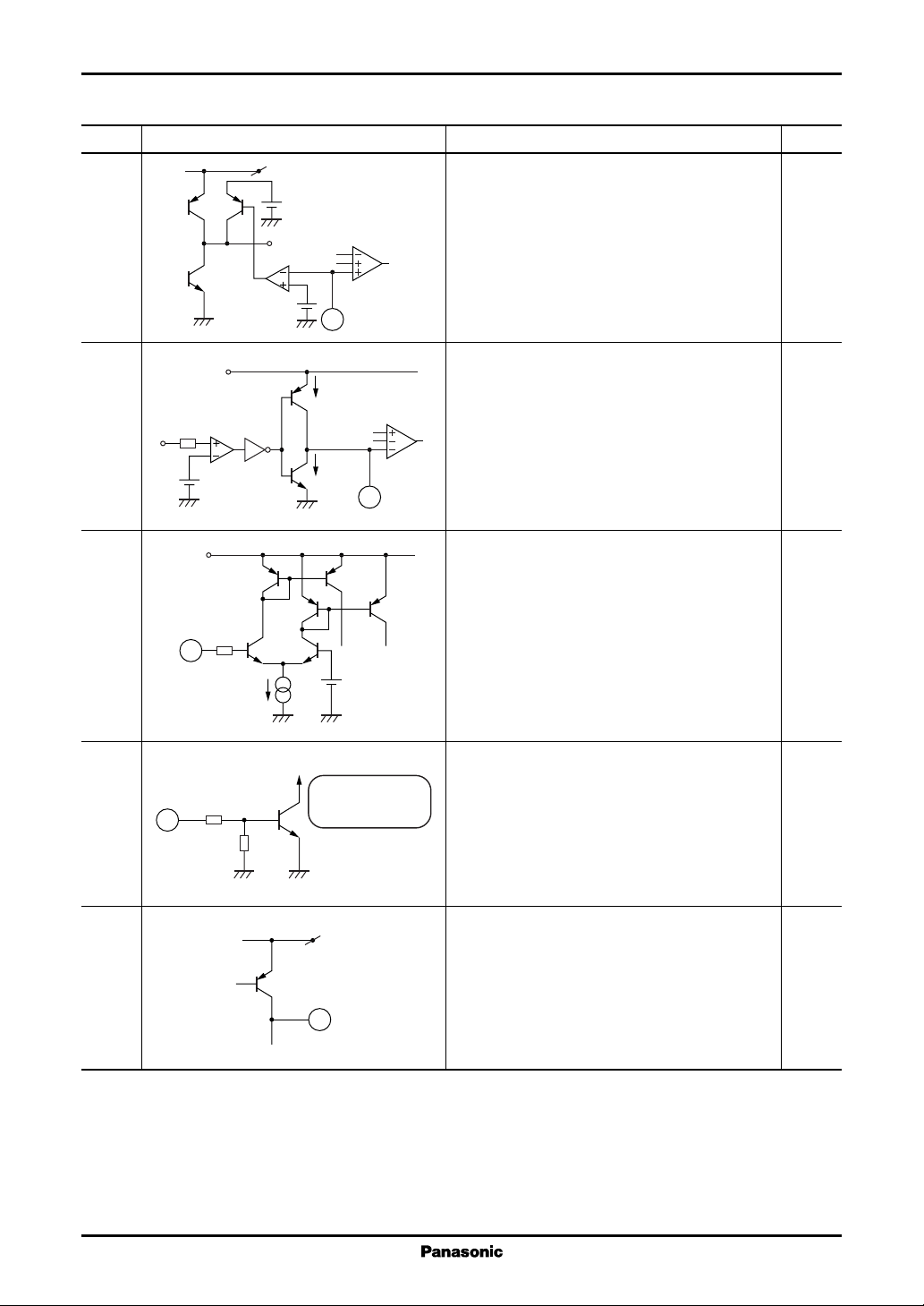
■ Terminal Equivalent Circuits (continued)
Pin No. Equivalent circuit Description I/O
12 DT2: I
V
FB2
0.9 V
CC
0.9 V
OSC PWM
12
The pin for setting channel 2 output maximum
duty ratio.
If this terminal is set at a voltage of 0.9 V or more,
FB2 terminal becomes high-level voltage and the
protective function for channel 2 output shortcircuit will stop (Unlatch function).
13 FB2: O
V
IN+2
CC
47 µA
OSC PWM
The output pin for error amplifier 2 block.
The source current is −47 µA and the sink current
is 47 µA.
Correct the frequency characteristics of the gain
1.19 V
47 µA
13
14 IN+2: I
V
CC
and the phase by connecting a resistor and a capacitor between this terminal and GND.
The noninverting input pin for error amplifier 2
block.
14
100 Ω
1.19 V
15 Off: I
The terminal for on/off control.
High-level input: Normal operation (V
V)
Low-level input: Standby state (V
< 0.8 V)
OFF
OFF
> 1.3
15
30 kΩ
60 kΩ
Internal circuit
start/stop
The total current consumption in the standby state
can be suppressed to a value 1 mA or less.
16 V
V
CC
:O
REF
The output terminal for the internal reference
voltage.
The reference voltage is 1.19 V (allowance: ± 2 %) at
16
= 2.4 V and I
CC
= − 0.1 mA.
REF
V
Connect a capacitor of 0.01 µF or more between
V
and GND for phase compensation.
REF
8
 Loading...