

Panasonic AN8015SH Datasheet
Voltage Regulators
AN8015SH
Single-channel step-down, step-up, or inverting use
DC-DC converter control IC
■ Overview
The AN8015SH is a single-channel DC-DC converter
control IC using the PWM method.
This IC can provide any one output type from among
step-down, step-up and inverting output.
Its operating supply voltage range is wide and its
consumption current is small. In addition, since it uses the
10-pin surface mounting type package with 0.5 mm pitch,
it is suitable for highly efficient miniature potable power
supply, especially for a negative output power supply.
■ Features
• Wide operating supply voltage range (3.6 V to 34 V)
• Small consumption current (1.8 mA typical)
• Converter control in a wide output frequency range is
possible (2 kHz to 500 kHz).
• Built-in timer latch short-circuit protection circuit (charge current 1.1 µA typical)
• Incorporating the under-voltage lock-out (U.V.L.O.) circuit
• Incorporating a high precision reference voltage circuit (2.46 V (allowance: ± 3%))
• Output block is open-collector (darlington) type.
• High absolute maximum rating of output current (100 mA)
• Maximum duty ratio is fixed and has small sample-to-sample variations (90% ± 5%).
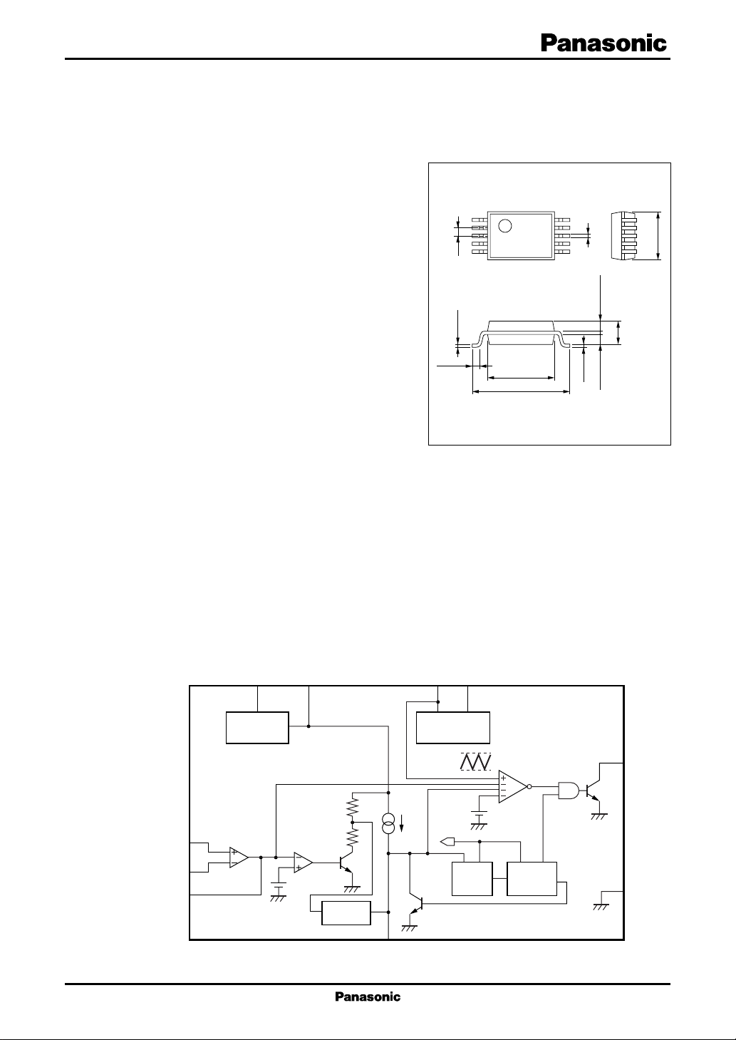
• Using 10-pin small outline package of 0.5 mm pitch
0.5±0.2
1
5
0.5
0.1±0.1
4.3±0.30
6.3±0.30
SSOP010-P-0225
10
6
+0.1
–0.05
0.15
Unit: mm
0.2±0.1
0.625±0.100.625±0.10
3.0±0.30
1.5±0.2
■ Applications
• LCD displays, digital still cameras, and PDAs
■ Block Diagram
IN+
IN−
FB
Error amp.
8
9
10
CC
V
6
Reference
supply
2.46 V
(allowance : ± 3%)
S.C.P. comp.
1.83 V
REF
V
7
CT1RT
2
0.5 V
Triangular
wave OSC
I
1.2 V
0.37 V
V
REF
SR
Latch
PWM
comparator
1.11 V
RO
U.V.L.O.
5
4
Out
GND
Clamp
3
S.C.P.
1
AN8015SH Voltage Regulators
■ Pin Descriptions
Pin No. Symbol Description
1 CT Pin for connecting oscillator timing capacitor
2 RT Pin for connecting oscillator timing resistor
3 S.C.P. Pin for connecting the time constant setting capacitor for short-circuit protection
4 GND Grounding pin
5 Out Open collector type output pin
6VCCPower supply voltage application pin
7V
REF
8IN+ Error amplifier noninverted input pin
9IN− Error amplifier inverted input pin
10 FB Output pin of error amplifier
■ Absolute Maximum Ratings
Parameter Symbol Rating Unit
Supply voltage V
IN− terminal allowable application voltage V
IN+ terminal allowable application voltage V
Output terminal allowable application voltage V
Collector output current I
Power dissipation
Operating ambient temperature
Storage temperature
Note)*: Expect for the power dissipation, operating ambient temperature, and storage temperature, all ratings are for Ta = 25°C.
Reference voltage output pin
*
*
*
OUT
P
T
T
CC
IN−
IN+
OUT
D
opr
stg
35 V
− 0.3 to V
− 0.3 to V
REF
REF
35
100 mA
154 mW
−30 to +85 °C
−55 to +150 °C
■ Recommended Operating Range
Parameter Symbol Range Unit
Error amplifier input voltage V
Collector output voltage V
Collector output current I
Timing capacitance C
Timing resistance R
Oscillation frequency f
Reference voltage output current I
Soft start short-circuit protection time C
constant setting capacitance
2
OUT
OUT
OUT
RE
SCP
IN
− 0.1 to 0.8 V
34 (maximum) V
50 (maximum) mA
T
T
100 to 27 000 pF
5.6 to 15 kΩ
2 to 500 kHz
−3 to 0 mA
1 000 (minimum) pF
Voltage Regulators AN8015SH
■ Electrical Characteristics at VCC = 12 V, RT = 15 Ω, CT = 200 pF, Ta = 25°C
Parameter Symbol Conditions Min Typ Max Unit
Reference voltage block
Reference voltage V
Input regulation with input fluctuation
Input regulation with input fluctuation 2
REFIREF
Line
Line2 VCC = 3.6 V to 20 V 10 mV
Load regulation Load I
Output voltage temperature V
TC1
characteristics 1
Output voltage temperature V
TC2
characteristics 2
Reference short-circuit current I
RS
U.V.L.O. block
Circuit operation start voltage V
Hysteresis width V
UON
HYS
Error amplifier block
Input offset voltage V
Input bias current I
Common-mode input voltage range V
High-level output voltage V
Low-level output voltage V
Output sink current I
Output source current I
Open-loop gain A
IO
B
ICR
EH
EL
SINK
SOURCEVFB
V
Common-mode ripple rejection ratio CMRR 50 dB
Output block
Oscillation frequency f
Maximum duty ratio Du
Output saturation voltage V
Output leak current I
RT terminal voltage V
Maximum oscillation frequency f
Frequency supply voltage f
OUT
maxRT
OLIO
LEAKVCC
RT
OUT(max)RT
dV
characteristics VCC = 3.6 V to 34 V
Frequency temperature characteristics 1
Frequency temperature characteristics 2
f
dT1fOUT
f
dT2fOUT
= −1 mA 2.386 2.46 2.534 V
VCC = 3.6 V to 34 V, I
= − 0.1 mA to −1 mA 210mV
REF
= −1 mA
REF
520mV
Ta = −30°C to +25°C ± 0.5 %
Ta = 25°C to 85°C ± 0.5 %
−20 mA
2.8 3.1 3.4 V
100 200 300 mV
−6 6mV
−500 −25 nA
− 0.1 0.8 V
V
− 0.3 V
− 0.1
REF
REF
V
0.1 0.3 V
VFB = 0.8 V 8 mA
= 0.8 V −120 µA
70 dB
RT = 15 kΩ, CT = 200 pF 175 195 215 kHz
= 15 kΩ, CT = 200 pF 85 90 95 %
= 50 mA, RT = 15 kΩ0.9 1.2 V
= 34 V, 10 µA
when output transistor is off
0.5 V
= 5.6 kΩ, CT = 150 pF 500 kHz
f
= 200 kHz, ±2 %
OUT
= 200 kHz,
±3 %
Ta = −30°C to +25°C
= 200 kHz,
±3 %
Ta = 25°C to 85°C
3
AN8015SH Voltage Regulators
■ Electrical Characteristics at VCC = 12 V, RT = 15 Ω, CT = 200 pF, Ta = 25°C (continued)
Parameter Symbol Conditions Min Typ Max Unit
Short-circuit protection circuit block
Input threshold voltage V
Input standby voltage V
Input latch voltage V
Charge current I
Comparator threshold voltage V
THPC
STBY
IN
CHG
THL
V
= 0 V −1.32 −1.1 − 0.88 µA
SCP
Whole device
Total consumption current I
Total consumption current 2 I
RT = 15 kΩ1.8 2.8 mA
CC
RT = 5.6 kΩ, CT = 150 pF 2.5 mA
CC2
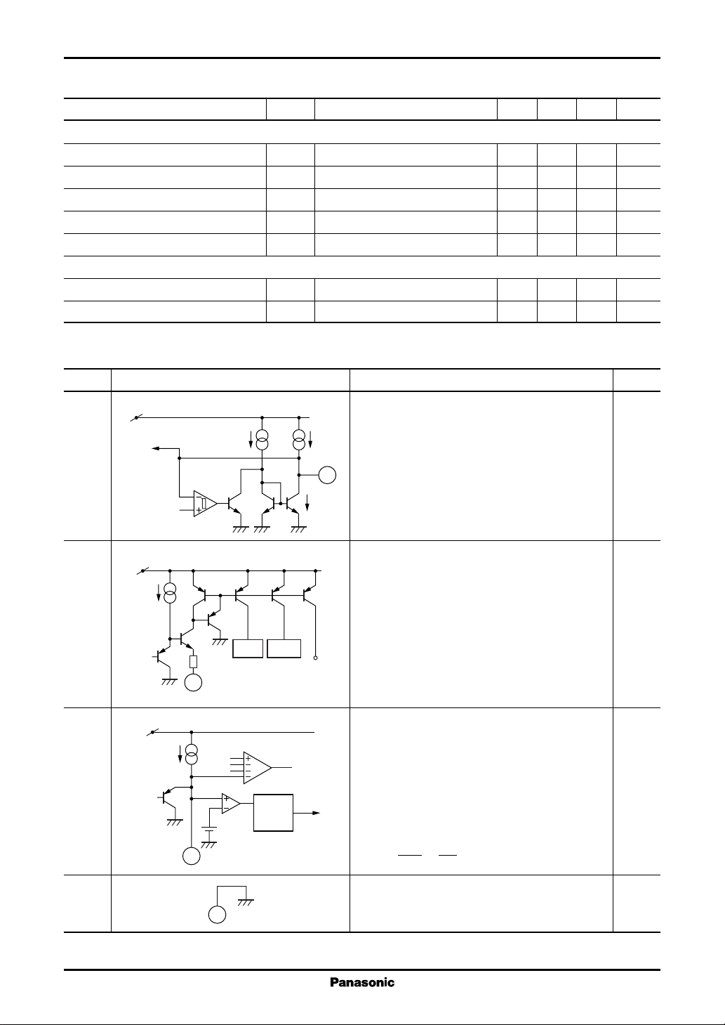
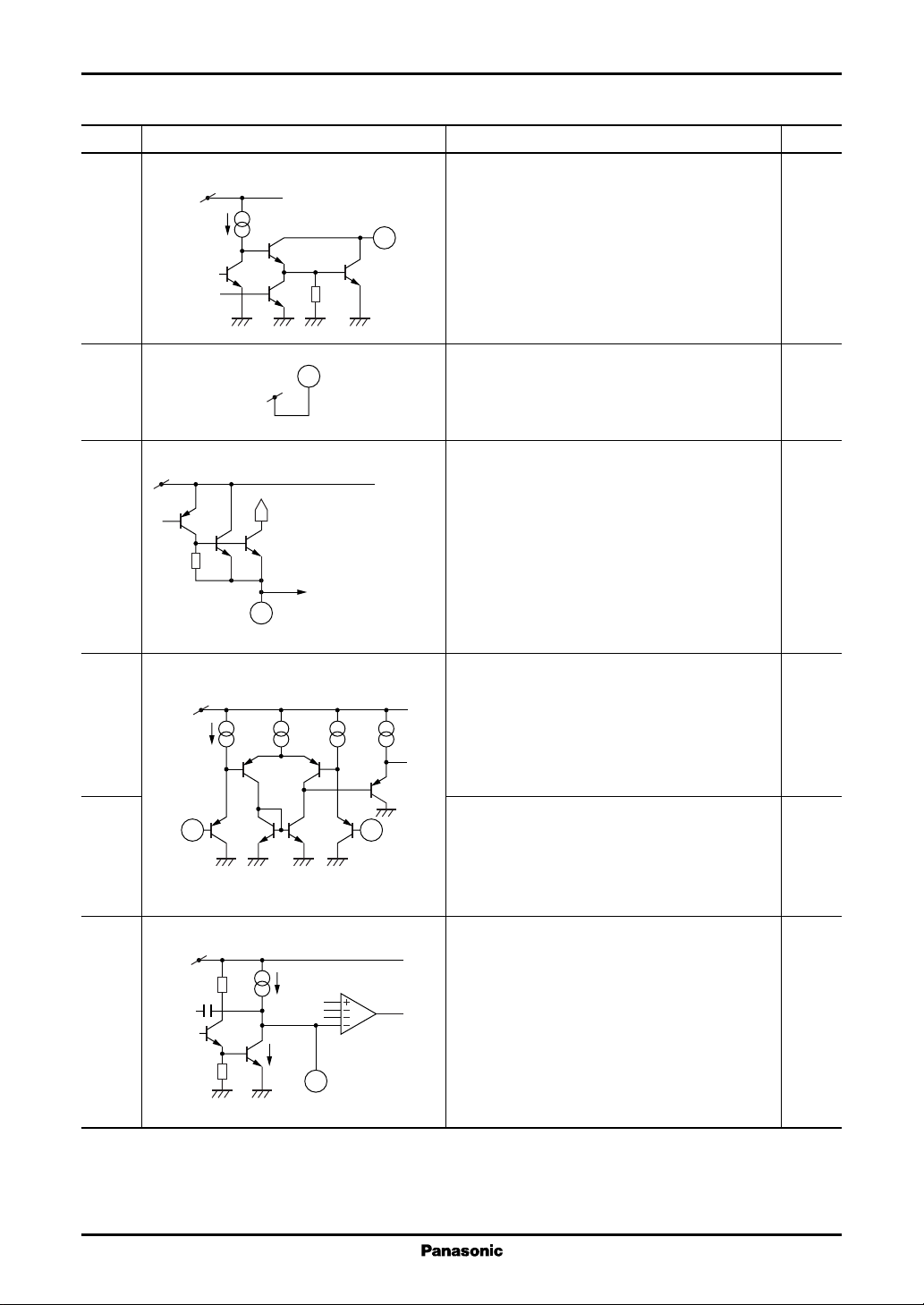
■ Terminal Equivalent Circuits
Pin No. Equivalent circuit Description I/O
1 CT: O
V
REF
To PWM input
OSC
comp.
210
The terminal used for connecting a timing capacitor to set oscillation frequency.
I
O
Use a capacitance value within the range of 100 pF
to 27 000 pF.
1
Use a oscillation frequency in the range of 2 kHz
to 500 kHz.
1.73 1.83 1.93 V
1.15 1.25 1.35 V
30 120 mV
1.83 V
2 RT: I
V
REF
The terminal used for connecting a timing resistor
to set oscillation frequency.
Use a resistance value within the range of 5.6 kΩ
to 15 kΩ . The terminal voltage is 0.5 V typ.
OSC PWM
100 Ω
2
RT(VRT ≈ 0.5 V)
3 S.C.P.: O
V
REF
S.C.P.
The terminal used for connecting a capacitor to set
I
CHG
CT
PWM
the time constant of soft start and timer latch shortcircuit protection circuit.
S.C.P.
Latch
S
Q
R
1.83 V
3
Use a capacitance value in the range of more than
1 000 pF.
The charge current is about 1.1 mA at R
V
I
CHG
RT
=
R
T
×1[A]
30
= 15 kΩ
T
4 GND:
Grounding terminal
4
4
Voltage Regulators AN8015SH
■ Terminal Equivalent Circuits (continued)
Pin No. Equivalent circuit Description I/O
5 Out: O
V
REF
Open-collector type (darlington) output terminal.
The absolute maximum rating of output current is
5
100 mA
Use with a steady-state output current under 50
mA.
6V
6
:
CC
The terminal for applying supply voltage.
Use with a operating supply voltage within the
range of 3.6 V to 34 V.
7V
V
CC
V
overcurrent detection
REF
:O
REF
The output terminal for the reference voltage (2.46
V)
Use with a load current −3 mA or under.
This terminal is incorporating the short-circuit
Bias to other block
7
protection circuit, and the short-circuit current is
about −20 mA. Use the V
for the reference
REF
input setting of the error amplifier.
8IN+:I
V
REF
The noninverted input terminal of the error amplifier.
For common-mode input, use in the range of − 0.1
V to +0.8 V.
9IN−:I
89
The inverted input terminal of the error amplifier.
For common-mode input, use in the range of − 0.1
V to +0.8 V.
10 FB: O
V
REF
120 µA
CT
PWM
The output terminal of the error amplifier.
The source current is about −120 µA, and the sink
current is about 8 mA.
Correct the frequency characteristics of the gain
8 mA
10
and the phase by connecting a resistor and a capacitor between this terminal and IN− terminal.
5
 Loading...