

Panasonic AN8014S Datasheet
Voltage regulators
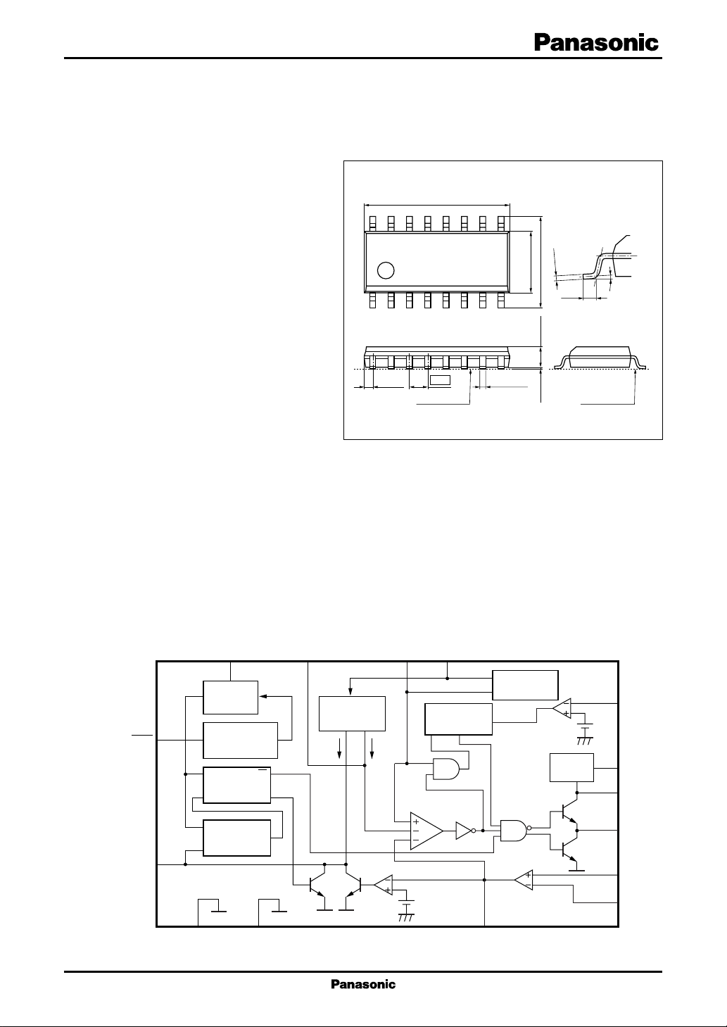
0.3
(0° to 10°)
(0.15)
10.1±0.3
4.2±0.3
6.5±0.3
18
16 9
1.27
(0.605)
Seating plane Seating plane
0.40±0.25
0.1±0.1 1.5±0.2
AN8014S
Step-down, step-up, or inverting DC-DC converter control IC
■ Overview
The AN8014S is a single-channel PWM DC-DC
converter control IC.
This IC can provide any one output type from
among step-down, step-up and inverting output.
Allowing n-channel power MOSFET direct driving, the AN8014S is ideal for high-efficiency power
supplies.
■ Features
• Wide operating supply voltage range (3.6 V to 34 V)
(The voltage is limited within a range between 3.6
V and 17 V if it is connected to a step-down voltage circuit.)
•
Totem pole output circuit: output peak current (±1 A)
• On-chip pulse-by-pulse overcurrent detection and
protection circuit
Threshold voltage V
− 0.095 V typical
CC
• On-chip bootstrap circuit (allowing n-channel MOSFET direct driving.)
• On-chip under-voltage lock-out circuit (U.V.L.O.)
• On-chip on/off function (active-high control input, standby current of maximum 5 µA)
• On-chip timer latch short-circuit protection circuit
• Maximum oscillator frequency (500 kHz)
SOP016-P-0225A
Unit: mm
■ Applications
• DC-DC switching power supply
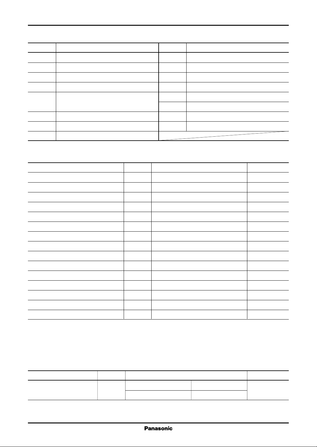
■ Block Diagram
16
OFF
5
S.C.P.
11
V
2.5V
On/off
active-high
R
U.V.L.O.
S
R
Latch
S
SGND
1
REF
V
REF
12
Q
Q
Q
PGND
DTC
4
Constant
current
source
1 µA 10 µA
S.C.P.
comp.
CT
3
2
Latch
RQS
PWM
comp.
RT
8
FB
Triangular
wave OSC
Error amp.
Boot
strap
10
CLM
15
V
CC
14
CB
13
Out
6
IN+
7
IN−
1
AN8014S Voltage regulators
■ Pin Descriptions
Pin No. Description
1 Internal reference output
2 Oscillator timing resistor connection
3 Oscillator timing capacitor connection
4 Dead-time control
5 Capacitance connection for short-circuit
protection delay
6 Error amplifier noninverting input
7 Error amplifier inverting input
8 Error amplifier output
■ Absolute Maximum Ratings
Parameter Symbol Rating Unit
Supply voltage V
Supply current I
2
Power dissipation
Operating ambient temperature
Storage temperature
*
1
*
1
*
On/off pin allowable application voltage V
Error amplifier allowable input voltage V
DTC pin allowable application voltage V
Out pin allowable application voltage V
Out pin constant output current I
Out pin peak output current I
CB pin allowable application voltage V
CB pin constant output current I
CB pin peak output current I
CLM pin allowable application voltage V
Note) 1.*1: Except for the operating ambient temperature and storage temperature, all ratings are for Ta = 25°C.
2: At Ta = 85°C
*
2. Do not apply external currents or voltages to any pins not specifically mentioned.
For circuit currents, '+' denotes current flowing into the IC, and '−' denotes current flowing out of the IC.
CC
CC
P
D
T
opr
T
stg
ON/OFF
I
DTC
OUT
O
O(Peak)
CB
CB
CBP
CLM
Pin No. Description
9 Not connected
10 Overcurrent protection input
11 Signal ground
12 Output stage ground
13 Totem pole type output
14 Bootstrap output
15 Supply voltage
16 On/off control
35 V
mA
143 mW
−30 to +85 °C
−40 to +125 °C
V
CC
− 0.3 to V
− 0.3 to V
REF
REF
35 V
±100 mA
±1 000 mA
35 V
−100, 150 mA
−500, 1 000 mA
V
CC
V
V
V
V
■ Recommended Operating Range
Parameter Symbol Range Unit
Supply voltage V
2
CC
Step-up circuit system 3.6 to 34 V
Step-down circuit system 3.6 to 17
Voltage regulators AN8014S
■ Electrical Characteristics at V
= 12 V, Ta = 25°C
CC
Parameter Symbol Conditions Min Typ Max Unit
Reference voltage block
Output voltage V
Line regulation with input fluctuation
REFIREF
Line VCC = 3.6 V to 34 V 16 25 mV
Load regulation Load I
U.V.L.O. block
Circuit operation start voltage V
Hysteresis width V
UON
HYS
Error amplifier block
Input offset voltage V
Input bias current I
Common-mode input voltage range V
High-level output voltage V
Low-level output voltage V
IO
B
ICR
EH
EL
Dead-time control circuit block
Input current I
Low-level input threshold voltage V
High-level input threshold voltage V
DTC
DT-L
DT-H
Output block
Oscillator frequency f
OUT
Output duty Du R
Low-level output voltage V
High-level output voltage V
OLIO
OHIO
Bootstrap circuit block
Input standby voltage V
INCBICB
Short-circuit protection circuit block
Input threshold voltage V
Input standby voltage V
Input latch voltage V
Charge current I
THPC
STBY
IN
CHG
On/off control block
Threshold voltage V
TH
Overcurrent protection block
Threshold voltage V
CLM
= −1 mA 2.522 2.6 2.678 V
= − 0.1 mA to −1 mA 110mV
REF
2.8 3.1 3.4 V
60 140 180 mV
−6 6mV
−500 −25 nA
− 0.1 0.8 V
V
REFVREF
V
− 0.3 − 0.1
0.1 0.3 V
−15.8 −13.2 −10.6 µA
Duty 0% 0.45 0.65 V
Duty 100% 1.2 1.4 V
CT = 120 pF, RT = 15 kΩ 196 218 240 kHz
= 75 kΩ 47 52 57 %
DTC
= 70 mA 1.0 1.3 V
= −70 mA V
CB
V
CB
V
−2.0 −1.0
= −70 mA V
CC
V
CCVCC
V
−1.2 −1.0 − 0.8
0.70 0.75 0.80 V
30 120 mV
30 120 mV
−2.76 −2.30 −1.84 µA
0.8 2.0 V
V
CC
V
CCVCC
V
− 0.115− 0.095− 0.075
3
AN8014S Voltage regulators
■ Electrical Characteristics at V
= 12 V, Ta = 25°C (continued)
CC
Parameter Symbol Conditions Min Typ Max Unit
Whole device
Total consumption current I
Standby current I
CC
CC(SB)
5.0 7.0 mA
5 µA
• Design reference data
Note) The characteristics listed below are theoretical values based on the IC design and are not guaranteed.
Parameter Symbol Conditions Limit Unit
Reference voltage block
Output voltage temperature V
Ta = −30°C to +25°C ±1%
TC1
characteristics 1
Output voltage temperature V
Ta = 25°C to 85°C ±1%
TC2
characteristics 2
Output short-circuit current I
OS
−40 mA
Error amplifier block
Output sink current I
Output source current I
SOURCEVFB
Open-loop gain A
SINKVFB
G
= 0.9 V 8 mA
= 0.9 V −110 µA
70 dB
Output block
f
Frequency supply voltage f
dV
= 200 kHz, ±3%
OUT
characteristics VCC = 3.6 V to 34 V
Frequency temperature f
dT1
f
= 200 kHz, ±9%
OUT
characteristics 1 Ta = −30°C to +25°C
f
Frequency temperature f
dT2
= 200 kHz, ±9%
OUT
characteristics 2 Ta = 25°C to 85°C
Oscillator block
RT pin voltage V
RT
0.4 V
Short-circuit protection circuit block
Comparator threshold voltage V
THL
1.87 V
Overcurrent protection circuit block
Delay time t
DLY
200 ns
4
Voltage regulators AN8014S
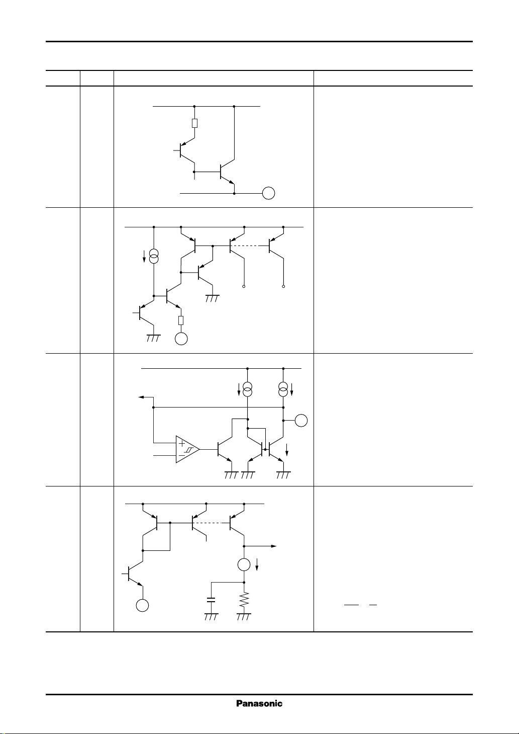
■ Terminal Equivalent Circuits
Pin No. I / O Equivalent circuit Description
1O V
V
CC
REF
:
Outputs the reference voltage
Incorporating short-circuit protection
against ground.
V
REF
1
2 RT:
V
REF
Connection for the timing resistor which
decides the oscillator frequency. Use a resistor in the range 5.1 kΩ to 30 kΩ. The
pin voltage is approx. 0.4 V.
DTC S.C.P.
100 Ω
RT(≈ 0.4 V)
2
3 CT:
V
REF
To PWM input
Connection for the timing capacitor which
decides the oscillator frequency. Use a ca-
I
O
pacitor in the range 100 pF to 10 000 pF.
CT
OSC
comp.
For the oscillator frequency setting, refer
3
to the "Application Notes, [1] Function
descriptions" section. Use an oscillator fre-
2I
O
quency in the range 5 kHz to 500 kHz.
2.6 V (allowance: 3%)
4 DTC:
V
REF
PWM comparator
input
Connection for a resistor and a capacitor
that set the dead-time and soft start period
of PWM output.
Input current I
I
4
R
DTC
DTC
DTC
C
DTC
2
resistor R
variations and temperature variations.
It is approx. −13.2 µA when RT = 15 kΩ.
I
DTC
RT
is decided by the timing
DTC
which controls sample to sample
T
× 1
V
RT
=
RT2
[A]
5
AN8014S Voltage regulators
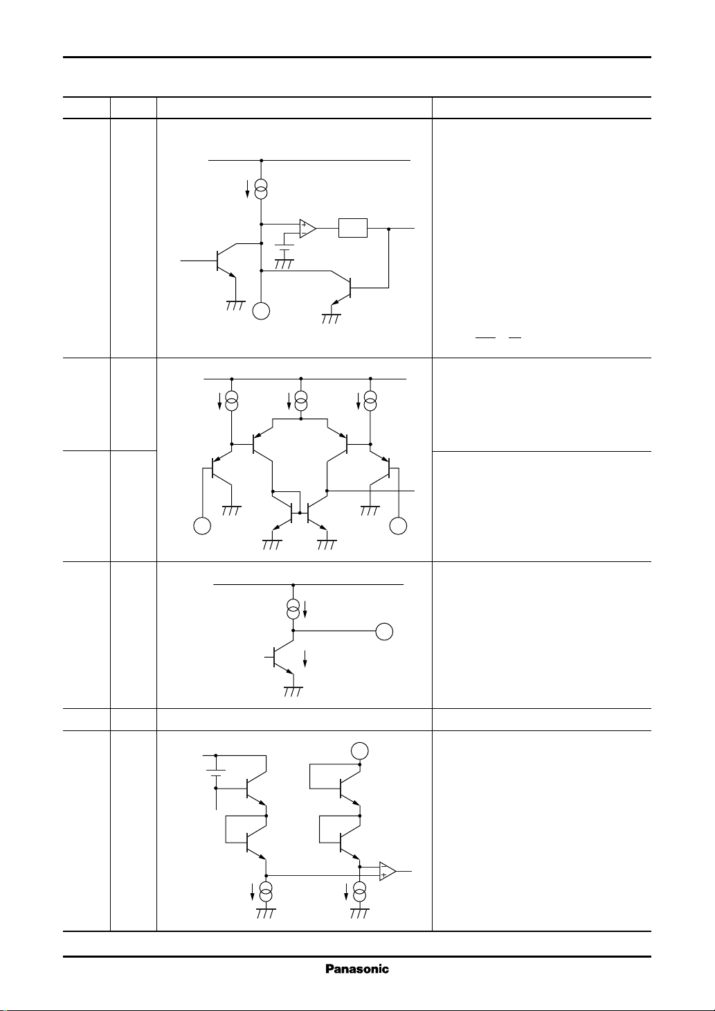
■ Terminal Equivalent Circuits (continued)
Pin No. I / O Equivalent circuit Description
5 S.C.P.:
V
REF
I
CHG
Latch
S
Q
U.V.L.O.
output
6I IN+:
V
REF
5
0.75 V
S.C.P.
R
Connection for the capacitor that sets the
soft start period and the timer latch shortcircuit protection circuit time constant.
Use a capacitor with a value of 1 000 pF
or higher.
The charge current I
timing resistor R
is decided by the
CHG
which controls sample
T
to sample variations and temperature variations.
It is approx. −2.3 µA when R
VRT × 1
I
CHG
=
RT11
[A]
= 15 kΩ.
T
Noninverting input to the error amplifier.
Use the common-mode input in the range
− 0.1 V to +0.8 V.
7I IN−:
Inverting input to the error amplifier.
Use the common-mode input in the range
− 0.1 V to +0.8 V.
7 6
IN− IN+
8 O FB:
V
REF
Source current
8
FB
Output from the error amplifier.
The source current is approx. −110 µA and
sink current is approx. 8 mA.
Correct the frequency characteristics of
Sink current
the gain and the phase by connecting a resistor and a capacitor between this pin
and IN− pin.
9 N.C.: Not connected.
10 I CLM:
V
CC
0.1 V
10
CLM
Detects the overcurrent state in switching
transistor.
Insert a resistor with a low resistance between
this pin and VCC to detect overcurrent states.
CLM
comp.
When this pin falls to a level 95 mV or
more lower than V
turned off for that period thus narrowing
50 µA 50 µA
the width of the on-period.
(This implements a pulse-by-pulse
overcurrent protection technique.)
, the PWM output is
CC
6
 Loading...