

Panasonic AN8013SH Datasheet
Voltage Regulators
AN8013SH
Single-channel step-up or step-down
DC-DC converter control IC
■ Overview
The AN8013SH is a single-channel PWM DC-DC
converter control IC. This IC implements DC-DC converters that provide a single arbitrary output voltage that
is either a stepped-up or stepped-down level. It features a
wide operating supply voltage range, low power, and a
built-in overcurrent protection circuit to protect the
switching transistor from damage or destruction. The
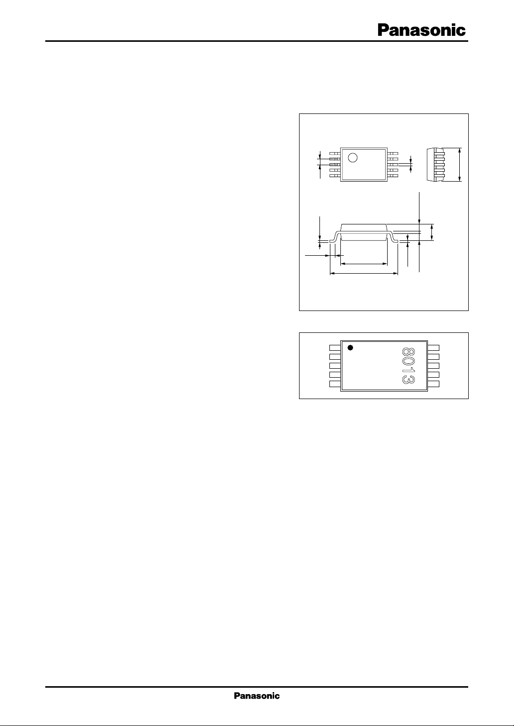
AN8013SH is provided in a 0.5 mm pitch 10-pin surface
mounting package and is optimal for use in miniature
high-efficiency portable power supplies.
0.5±0.2
Unit: mm
1
5
0.5
0.1±0.1
4.3±0.30
6.3±0.30
10
0.2±0.1
6
0.625±0.100.625±0.10
+0.1
–0.05
0.15
3.0±0.30
1.5±0.2
■ Features
• Wide operating supply voltage range (3.6 V to 34 V)
• Small consumption current (2.4 mA typical)
• Supports control over a wide output frequency range:
20 kHz to 500 kHz.
• Built-in pulse-by-pulse overcurrent protection circuit
(Detection voltage: V
− 100 mV)
CC
• Built-in timer latch short-circuit protection circuit
■ Pin Descriptions
CLM
RT
CT
S.C.P.
DTC
(charge current 1.3 µA typical)
• Incorporating the under-voltage lock-out (U.V.L.O.) circuit
• Built-in reference voltage circuit (Error amplifier reference input: 0.75 V (allowance: ±4%))
• Output block is open-collector (darlington) type.
• High absolute maximum rating of output current (100 mA)
• Duty ratio with small sample-to-sample variations (55% ± 5%).
• Adopts a 0.5-mm lead pitch 10-pin small outline package
SSOP010-P-0225
1
2
3
4
5
■ Applications
• Switching mode power supply units (in portable equipment and other applications)
10
V
CC
9
Out
8
GND
7
IN−
6
FB
1
AN8013SH Voltage Regulators
■ Block Diagram
CC
FB
IN−
V
6
Error amp.
7
V
10
REF
0.75 V
0.1 V
CLM
1
S.C.P. comp.
1.90 V
DTC
5
V
REF
R
S R
Latch
V
REF
R
T
4
S.C.P.
T
0.75 V
V
REF
S R
Latch
PWM
R
S Q
U.V.L.O.
CT3RT
2
OSC
9
Out
8
GND
■ Absolute Maximum Ratings at Ta = 25°C
Parameter Symbol Rating Unit
Supply voltage V
CLM pin allowable application voltage V
Error amplifier allowable input voltage V
DTC pin allowable input voltage V
Out pin allowable application voltage V
Collector output current I
Power dissipation (Ta = 85°C) P
Operating ambient temperature T
Storage temperature T
CC
CLM
IN−
DTC
OUT
OUT
D
opr
stg
35 V
35 V
−0.3 to +2.5 V
2.5 V
35 V
100 mA
154 mW
−30 to +85 °C
−55 to +150 °C
■ Recommended Operating Range at Ta = 25°C
Parameter Symbol Min Max Unit
Supply voltage rise time (0 to 3.6 V) tr (VCC)10 µs
Collector output voltage V
Collector output current I
Timing capacitance C
Timing resistance R
Oscillator frequency f
Short-circuit protection time constant setting C
capacitor
OUT
OUT
T
T
OUT
SCP
34 V
50 mA
100 1 800 pF
5.1 15 kΩ
20 500 kHz
1 000 pF
2
Voltage Regulators AN8013SH
■ Electrical Characteristics at Ta = 25°C
Parameter Symbol Conditions Min Typ Max Unit
U.V.L.O. block
Circuit operation start voltage V
Hysteresis width V
UON
HYS
Error amplifier block
Input threshold voltage V
Line regulation with input fluctuation V
Voltage follower 0.72 0.75 0.78 m V
TH
Voltage follower, 28mV
dv
VCC = 3.6 V to 34 V
Input bias current I
High-level output voltage V
Low-level output voltage V
Input threshold voltage temperature V
B
EH
EL
Voltage follower, ±1 %
dt1
characteristics 1 Ta = −30°C to +25°C
Input threshold voltage temperature V
Voltage follower, ±1 %
dt2
characteristics 2 Ta = −25°C to +85°C
Output sink current I
Output source current I
SOURCEVFB
Open-loop gain A
VFB = 0.9 V 8 mA
SINK
= 0.9 V −120 µA
V
PWM Comparator Block
Input threshold voltage: high V
Input threshold voltage: low V
Input current I
Duty: 100% 1.2 V
DT-H
Duty: 0% 0.6 V
DT-L
DTC
Output block
Oscillation frequency f
Output duty Du R
Output saturation voltage V
Output leak current I
RT pin voltage V
Maximum oscillation frequency f
OUT(max)RT
Frequency supply voltage f
RT = 15 kΩ, CT = 150 pF 185 205 225 kHz
OUT
= 91 kΩ 50 55 60 %
DTC
OLIO
LEAKVCC
RT
= 50 mA, RT = 15 kΩ0.9 1.2 V
= 34 V, when output Tr is off 10 µA
= 5.1 kΩ, CT = 120 pF 500 kHz
f
dV
= 200 kHz, ±1 %
OUT
characteristics VCC = 3.6 V to 34 V
Frequency temperature f
dT1fOUT
characteristics 1
Frequency temperature f
dT2fOUT
characteristics 2
Note)
At VCC = 12 V, RT = 15 kΩ, CT = 15 pF, unless otherwise specified.
= 200 kHz,
Ta = −30°C to +25°C
= 200 kHz,
Ta = 25°C to 85°C
2.8 3.1 3.4 V
100 200 300 mV
−500 −25 nA
2.0 V
0.3 V
70 dB
−12 −11 −10 A
0.59 V
±3 %
±3 %
3
V
CC
CLM
comp.
50 µA50 µA
0.1 V
1
AN8013SH Voltage Regulators
■ Electrical Characteristics at Ta = 25°C (continued)
Parameter Symbol Conditions Min Typ Max Unit
Short-circuit protection circuit block
Input threshold voltage V
Input standby voltage V
Input latch voltage V
Charge current I
Comparator threshold voltage V
THPC
STBY
IN
CHG
THL
V
= 0 V −1.6 −1.3 − 1.0 µA
SCP
Overcurrent Protection Block
Input threshold voltage V
Delay time t
CLM
DLY
Whole device
Total consumption current 1 I
Total consumption current 2 I
Note)
At VCC = 12 V, RT = 15 kΩ, CT = 15 pF, unless otherwise specified.
RT = 15 kΩ2.4 3.5 mA
CC
RT = 5.1 kΩ, CT = 150 pF 3.4mA
CC2
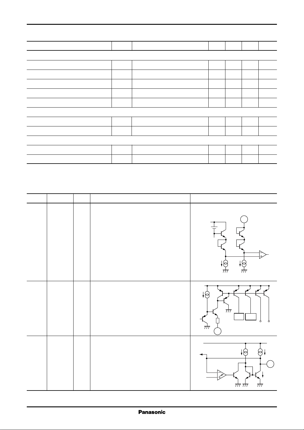
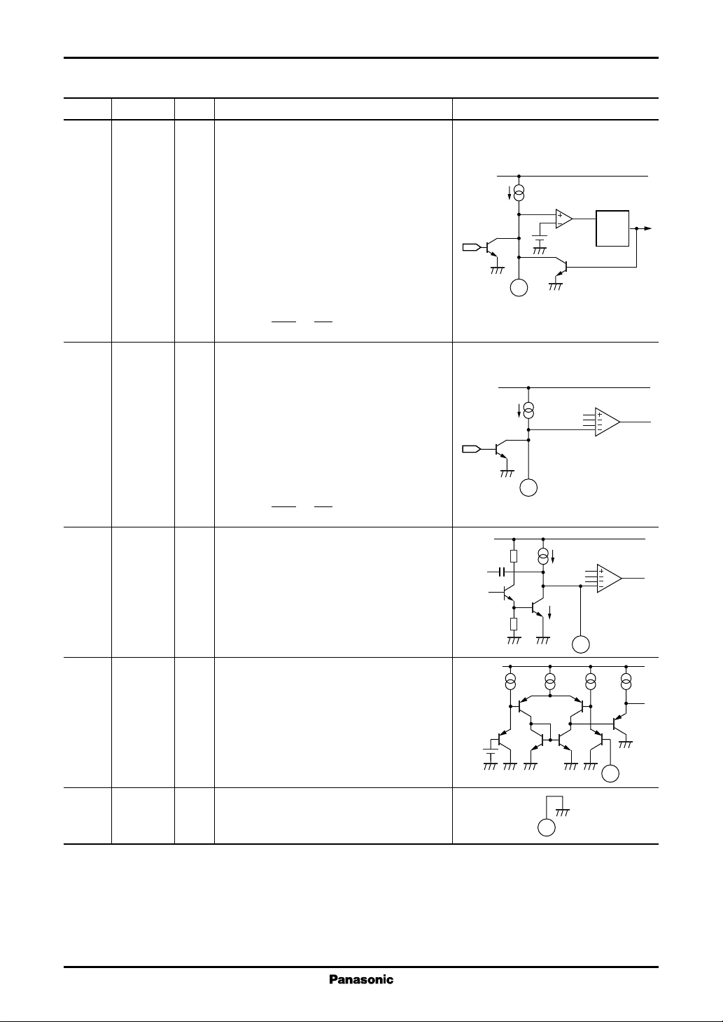
■ Terminal Equivalent Circuits
Pin No. Pin I/O Function Internal equivalent circuit
1 CLM I Detects the overcurrent state in switching
transistor.
Insert a resistor with a low resistance between
this pin and V
When this pin falls to a level 100 mV or more
lower than VCC, the PWM output is turned off
for that period thus narrowing the width of
the on period.
(This implements a pulse-by-pulse
overcurrent protection technique.)
2 RT I Connection for the timing resistor that deter-
mines the oscillator frequency.
Use a resistor in the range 5.1 kΩ to 15 kΩ.
Thus the pin voltage will be about 0.59 V.
3 CT O Connection for the timing capacitor that
determines the oscillator frequency.
Use a capacitor in the range 100 to 1 800 pF.
See the "Application Notes, [2] and [3]"
sections later in this document for details on
setting the frequency. Use an oscillator
frequency in the range 20 kHz to 500 kHz.
to detect overcurrent states.
CC
V
V
To PWM input
0.70 0.75 0.80 V
120 V
120 mV
1.90 V
VCC − 120 VCC − 100 VCC − 80
200 ns
REF
100 Ω
RT (V ≈ 0.59 V)
2
REF
OSC
comp.
OSC PWM
S.C.P.
mV
DTC
2I
I
O
3
O
4
Voltage Regulators AN8013SH
■ Terminal Equivalent Circuits (continued)
Pin No. Pin I/O Function Internal equivalent circuit
4 S.C.P. O Connection for the capacitor that determines
the time constant for soft start and the timer
latch short-circuit protection circuit.
Use a capacitor with a value of 1 000 pF or
higher.
The charge current I
is determined by the
CHG
timing resistor RT, and sample-to-sample and
temperature variations can be suppressed.
When R
is 15 kΩ, the current will be about
T
−1.3 µA.
I
CHG
V
=
R
RT
1
×
[A]
30
T
5 DTC I Connection for the resistor and capacitor that
determine the PWM output dead-time and the
soft start period.
The input current I
is determined by the
DTC
timing resistor RT, and sample-to-sample and
temperature variations can be suppressed.
When R
is 15 kΩ, the current will be about
T
−11 µA.
I
CHG
V
=
R
RT
1
×
[A]
3.6
T
6 FB O Error amplifier output
A source current is about −120 mA and a sink
current is about 8 mA.
Correct the gain and the phase frequency
characteristics by inserting a resistor and a
capacitor between this pin and IN−pin.
7IN− I Error amplifier inverting input
For common-mode input, use in the range
− 0.1 V to +0.8 V.
V
REF
U.V.L.O.
V
REF
U.V.L.O.
V
REF
V
REF
I
CHG
0.75 V
Latch
S
R
Q
4
I
DTC
CT
PWM
5
120 µA
8 mA
PWM
C
T
6
8 GND Ground
0.75 V
7
8
5
 Loading...