

Voltage Regulators
0.3
(0° to 10°)
(0.15)
10.1±0.3
4.2±0.3
6.5±0.3
18
16 9
1.27
(0.605)
Seating plane Seating plane
0.40±0.25
0.1±0.1 1.5±0.2
AN8011S
2-channel step-down, step-up, or inverting use
DC-DC converter control IC
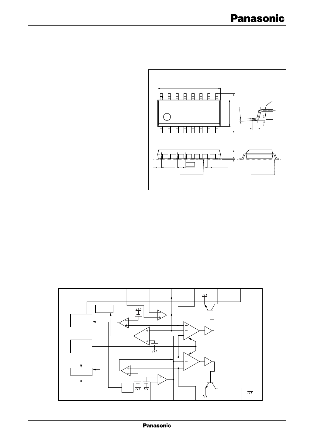
Unit: mm
■ Overview
The AN8011S is a DC-DC converter control IC
with two-channel output using the PWM method
which allows 500 kHz high-speed control.
Respecitve output operation can be completely
synchronized with each other by using the same
oscillation output.
■ Features
• PWM control frequency of 500 kHz is available.
• Wide operating supply voltage range
(V
= 3.6 V to 34 V)
CC
• Built-in 2-channel of open collector type for out-
put (A single-channel is also usable for inverted
amplification type)
• Each output can be stopped independently by the
external control .
• Built-in on/off function for the operation/stop of IC Incorporating circuit for short-circuit portection and under-
voltage lock-out (U.V.L.O.)
• The latch circuit is externally controllable.
• Low consumption current (during operation: 5 mA, during standby: 2 µA)
SOP016-P-0225A
■ Applications
• LCD displays, digital still cameras, and PDAs
■ Block Diagram
REF
V
16
V
REF
U.V.L.O.
OSC
1
CT
Latch
15
Latch
2
RT
IN+
14
Unlatch pro.
Short pro.
Unlatch pro.
On/
Off
3
On/Off
IN−1
13
Error amp.
Error amp.
4
IN−2
12
FB1
5
FB2
11
PWM1
PWM2
6
DTC1
DTC2
10
7
Out1
Out2
9
8
CC
V
GND
1
AN8011S Voltage Regulators
■ Pin Descriptions
Pin No. Symbol Description
1 CT Pin for connecting the oscillation frequency setting capacitor for triangular oscillation
circuit. Frequecy of triangular oscillation is set by connecting a capacitor between this
terminal and GND.
2 RT Resistor connection pin for setting the oscillation frequency of triangular oscillation
circuit. Frequecy of triangular oscillation is set by connecting resistance between the
pin and GND
3 On/Off "On/Off" pin for turning on/off IC. "Low" stops IC (output off) and "High" operates IC.
4IN−2 Inverted input pin for channel 2 error amplifier
5 F/B 2 Output pin for channel 2 error amplifier. Gain setting or phase compensation is per-
formed by connecting resistor or capacitor between the pin and IN−2. It is also connected
to PWM short-circuit protecion.
6 DTC 2 Pin for setting dead-time period of channel 2. The dead-time of channel 2 is set by
connecting external resistor. Soft start function can be also given by connecting capacitor in parallel with the external resistor. In addition, only channel 2 output can be turned
off by decreasing the pin voltage to below 0.12 V. (short-circuit protection function stop
circuit)
7 Out 2 Channel 2 open-collector type output pin. IO = 100 mA maximum
8 GND Grounding pin of signal system.
9VCCPower supply voltage application pin. It detects start voltage and stop voltages
10 Out 1 Channel 1 open-collector type output pin. IO = 100 mA maximum
11 DTC 1 Pin for setting dead-time period of channel 1. The dead-time period of channel 1 is set
by connecting external resistor. Soft start function can be also given by connecting capacitor
in parallel with the external resistor. In addition, only channel 1 output can be turned off
by decreasing the pin voltage to below 0.12 V. (short-circuit protection function stop
circuit)
12 F/B 1 Output pin for channel 1 error amplifier. Gain setting or phase compensation is per
formed by connecting resistor or capacitor between the pin and IN−1. It is also con
nected to PWM short-circuit protection.
13 IN−1 Inverted input pin for channel 1 error amplifier.
14 IN+ Pin for noninverted input of channel 1error amplifier.
15 Latch Pin for connecting the time constant setting capacitor for timer latch type short-circuit
protection circuit. The time constant for short-circuit protection is set by connecting
a capacitor between this terminal and GND.
16 V
REF
Internal reference voltage output pin (2.5 V(allowance: ±3%)). If a load of 20 mA typical
or more is applied, the overcurrent protection operates to reduce V
and switching
REF
operation stops.
2
Voltage Regulators AN8011S
■ Absolute Maximum Ratings at Ta = 25°C
Parameter Symbol Rating Unit
Supply voltage V
Power dissipation
*
Operating ambient temperature T
Storage temperature T
Note) 1 . Do not apply ecternal currents or voltages to any pins not speifically mentioned.
For circuit currents, '+' denotes current flowing into the IC, and '−' denotes current flowing out of the IC.
2*: When using the IC at Ta of 25°C or more, the power dessipation should be decreased 3.8 mW per 1°C.
CC
P
D
opr
stg
■ Recommended Operating Range
Parameter Symbol Range Unit
Supply voltage V
CC
■ Electrical Characteristics at VCC = 12 V, Ta = 25°C
Parameter Symbol Conditions Min Typ Max Unit
Reference voltage block
Output voltage V
Input regulation with input fluctuation Line VCC = 3.6 V to 34 V 320mV
Load regulation Load I
Output voltage temperature V
characteristics 1
*
Output voltage temperature V
characteristics 2
*
Overcurrent protection drive current *I
U.V.L.O. block
Circuit operation start voltage V
Hysteresis width V
Error amplifier block 1
Input offset voltage 1 V
Input current 1 I
Common-mode input voltage range V
High-level output voltage 1 V
Low-level output voltage 1 V
Error amplifier block 2
Input current 2 I
Common mode input threshold voltage
High-level output voltage 2 V
Low-level output voltage 2 V
REF
= 0 mA to 5 mA 210mV
REF
TC1Ta
TC2Ta
CC
UON
HYS
IN-O1
B1
CM
EH1
EL1
B2
= −25°C to + 25°C ±1 %
= 25°C to 85°C ±1 %
VIN+ 0.72 0.75 0.78 V
EH2
EL2
35 V
380 mW
−30 to +85 °C
−40 to +125 °C
3.6 to 34 V
2.413 2.5 2.588 V
−20 mA
2.8 3.1 3.4 V
100 200 300 mV
−6 6mV
−500 −25 100 nA
0.5 0.8 V
V
− 0.3
REF
V
0.5 V
25 100 nA
V
− 0.3
REF
V
0.5 V
3
AN8011S Voltage Regulators
■ Electrical Characteristics(continued) at VCC = 12 V, Ta = 25°C
Parameter Symbol Conditions Min Typ Max Unit
PWM comparator 1/2 block
High-level input threshold voltage V
Low-level input threshold voltage V
Input current I
DT-HfOSC
DT-LfOSC
DTC
Output 1/2 block
Output frequency 1 f
Frequency 1 f
OUT1CT
dv
Output duty ratio 1 Du1CT = 150 pF, RT = 20 kΩ, R
Output duty ratio 2 Du2CT = 150 pF, RT = 20 kΩ, R
Output saturation voltage 1 V
Output saturation voltage 2 V
Output leak current 1 I
Frequency temperature characteristics 1 *f
Frequency temperature characteristics 2 *f
Output frequency 2
Frequency 2
*
*
O(sat)1IO
O(sat)2IO
OLe1
dT1fOSC
dT2fOSC
f
OUT2CT
f
dv2
Short-circuit protection block
Input threshold voltage V
Latch drive voltage V
Charge current
SLTH
SLON
I
CHG
Unlatch pro. 1/2 block
Input threshold voltage V
ULTH
On/off block
Threshold voltage V
TH
Whole device
Total consumption current
Total consumption current fluctuation
Standby consumption current I
Maximum standby consumption current I
Note)*: These characteristics are theoretical values based on the IC design and are not guaranteed.
I
CC
I
CC(max.)VCC
CC(SB)VCC
CC(SB-M)VCC
= 200 kHz, duty = 100% 1.2 V
= 200 kHz, duty = 100% 0.6 V
RT = 20 kΩ−37 −34 −31 µA
= 150 pF, RT = 20 kΩ, IO = 30 mA
180 200 220 kHz
VCC = 3.6 V to 34 V −2 2%
CT = 150 pF, RT = 20 kΩ
DTC
DTC
= 24 k Ω
= 33 k Ω
40 45 50 %
65 75 85 %
= 30 mA 0.9 V
= 100 mA 1.2 V
V
= 34 V, when output 10 µA
CC
transistor is off
= 200 kHz, Ta = −30°C to +25°C
= 200 kHz, Ta = 25°C to 85°C
= 150 pF, RT = 6.6 kΩ, IO = 30 mA
±9 %
±9 %
500 kHz
VCC = 3.6V to 34V, ±2 %
CT = 150 pF, RT = 6.6 kΩ
1.75 1.85 1.95 V
1.15 1.25 1.35 V
−120 −50 −40 µA
0.12 V
0.8 2V
VCC = 12 V, RT = 20 kΩ57mA
= 3.6 V to 34 V, RT = 20 kΩ 2mA
= 12 V, V
= 34 V, V
is down 2 µA
REF
is down 5 µA
REF
4
Voltage Regulators AN8011S
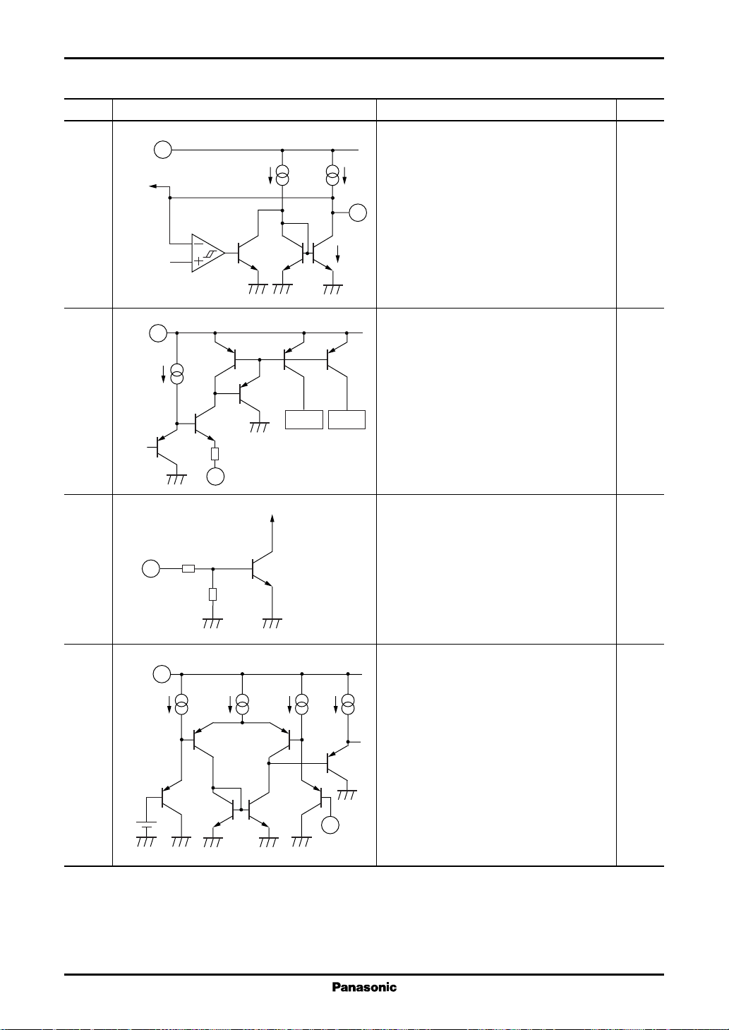
■ Terminal Equivalent Circuits
Pin No. Equivalent circuit Description I/O
1 CT: O
V
REF
16
To PWM input
OSC
comp.
2 RT: I
V
REF
16
OSC PWM
The terminal used for connecting a timing
capacitor to set oscillator frequency. Use a
I
O
capacitance value within the range of 100 pF
CT
to 0.1mF. For frequency setting method, re-
1
fer to the "Application Notes, [2] Function
descriptions" section. Use the oscillation fre-
2I
O
quency in the range of 1 kHz to 500 kHz.
The terminal used for connecting a timing
resistor to set oscillattion frequency.
Use a resistance value ranging from 5.1 kΩ
to 20 kΩ.
The terminal voltage is 0.67 V typ.
RT (= 0.67 V)
2
3 On/Off: I
The terminal for on/off control.
High-level input: normal operation
(V
ON/OFF
> 2.0 V typ.)
Low-level input: standby state
(V
ON/OFF
< 0.8 V typ.)
On/Off
3
Internal
circuit start/stop
17 kΩ
13 kΩ
The total current consumption in the standby
state can be suppressed to a value below 5 µA.
4IN−2: I
V
REF
16
The terminal for the inverted input of ch.2
error amplifier. Use a common-mode input
ranging from − 0.1 V to 0.8 V.
0.75 V
4
IN−2
5
 Loading...