

Panasonic 2SD1302 Datasheet
Transistor
V
B
IB=1mA
R
on
= ✕1000(Ω)
f=1kHz
V=0.3V
1kΩ
V
A
V
V
VA–V
B
V
B
2SD1302
Silicon NPN epitaxial planer type
For low-voltage output amplification
For muting
For DC-DC converter
Features
■
●
Low collector to emitter saturation voltage V
●
Low ON resistance Ron.
●
High foward current transfer ratio hFE.
Absolute Maximum Ratings (Ta=25˚C)
■
Parameter
Collector to base voltage
Collector to emitter voltage
Emitter to base voltage
Peak collector current
Collector current
Collector power dissipation
Junction temperature
Storage temperature
Electrical Characteristics (Ta=25˚C)
■
Parameter
Collector cutoff current
Collector to base voltage
Collector to emitter voltage
Emitter to base voltage
Forward current transfer ratio
Collector to emitter saturation voltage
Base to emitter saturation voltage
Transition frequency
Collector output capacitance
ON resistanse
*1
h
Rank classification
FE1
Rank R S T
h
FE1
200 ~ 350 300 ~ 500 400 ~ 800
Symbol
V
CBO
V
CEO
V
EBO
I
CP
I
C
P
C
T
j
T
stg
Symbol
I
CBO
V
CBO
V
CEO
V
EBO
*1
h
FE1
h
FE2
V
CE(sat)
V
BE(sat)
f
T
C
ob
*3
R
on
.
CE(sat)
Ratings
25
20
12
1
0.5
600
150
–55 ~ +150
Unit
V
V
V
A
A
mW
˚C
˚C
Conditions
VCB = 25V, IE = 0
IC = 10µA, IE = 0
IC = 1mA, IB = 0
IE = 10µA, IC = 0
VCE = 2V, IC = 0.5A
VCE = 2V, IC = 1A
*2
IC = 0.5A, IB = 20mA
IC = 0.5A, IB = 50mA
VCB = 10V, IE = –50mA, f = 200MHz
VCB = 10V, IE = 0, f = 1MHz
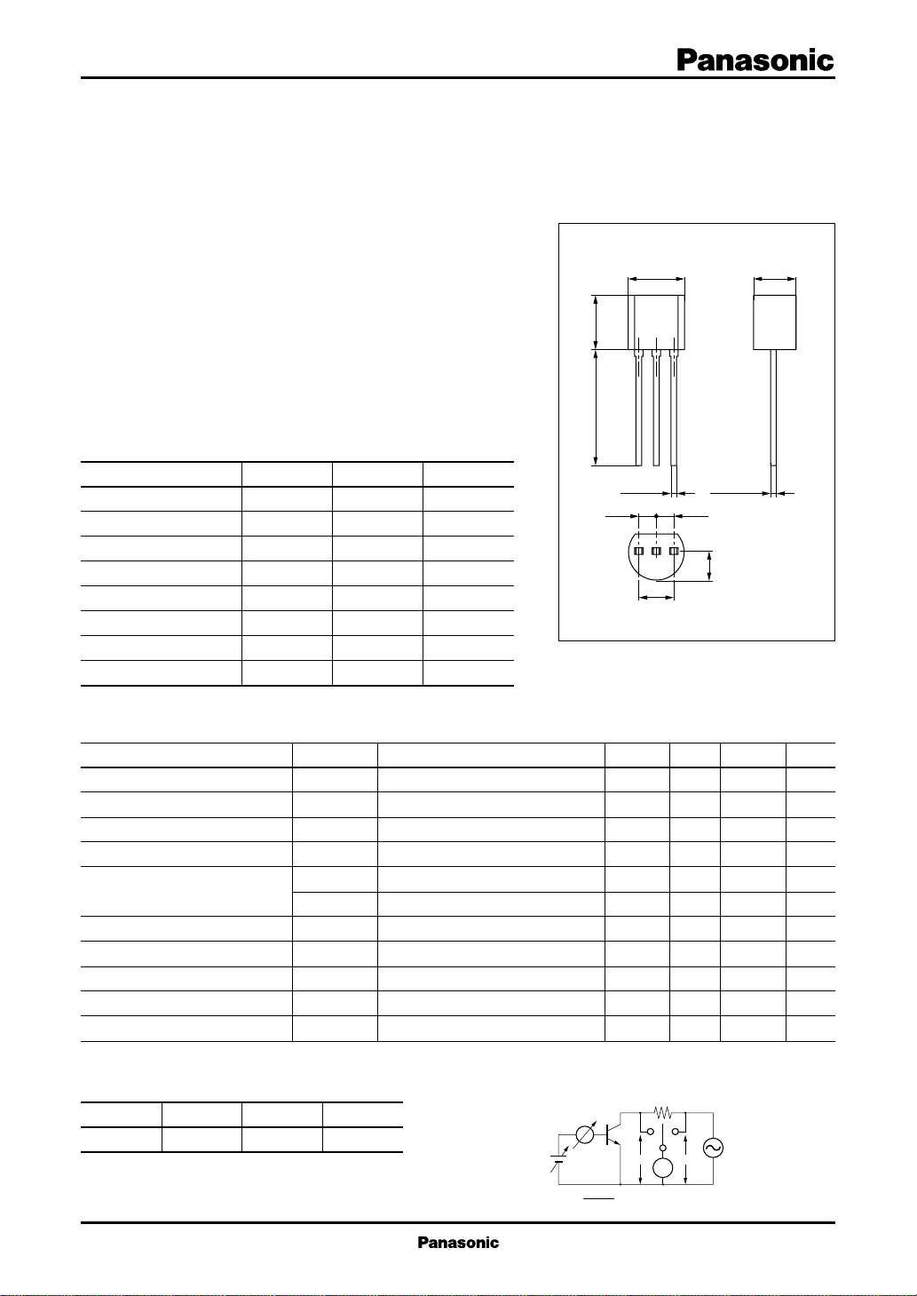
5.1±0.213.5±0.5
0.45
1.27 1.27
*2
*3
Ron Measurement circuit
5.0±0.2 4.0±0.2
typ
0.45
2.3±0.2
+0.2
–0.1
1:Emitter
2:Collector
3:Base
JEDEC:TO–92
EIAJ:SC–43A
max
+0.2
–0.1
213
2.54±0.15
min
100
25
20
12
200
800
60
0.13
0.4
1.2
200
10
1.0
*2
Pulse measurement
Unit: mm
Unit
nA
V
V
V
V
V
MHz
pF
Ω
1
Transistor
2SD1302
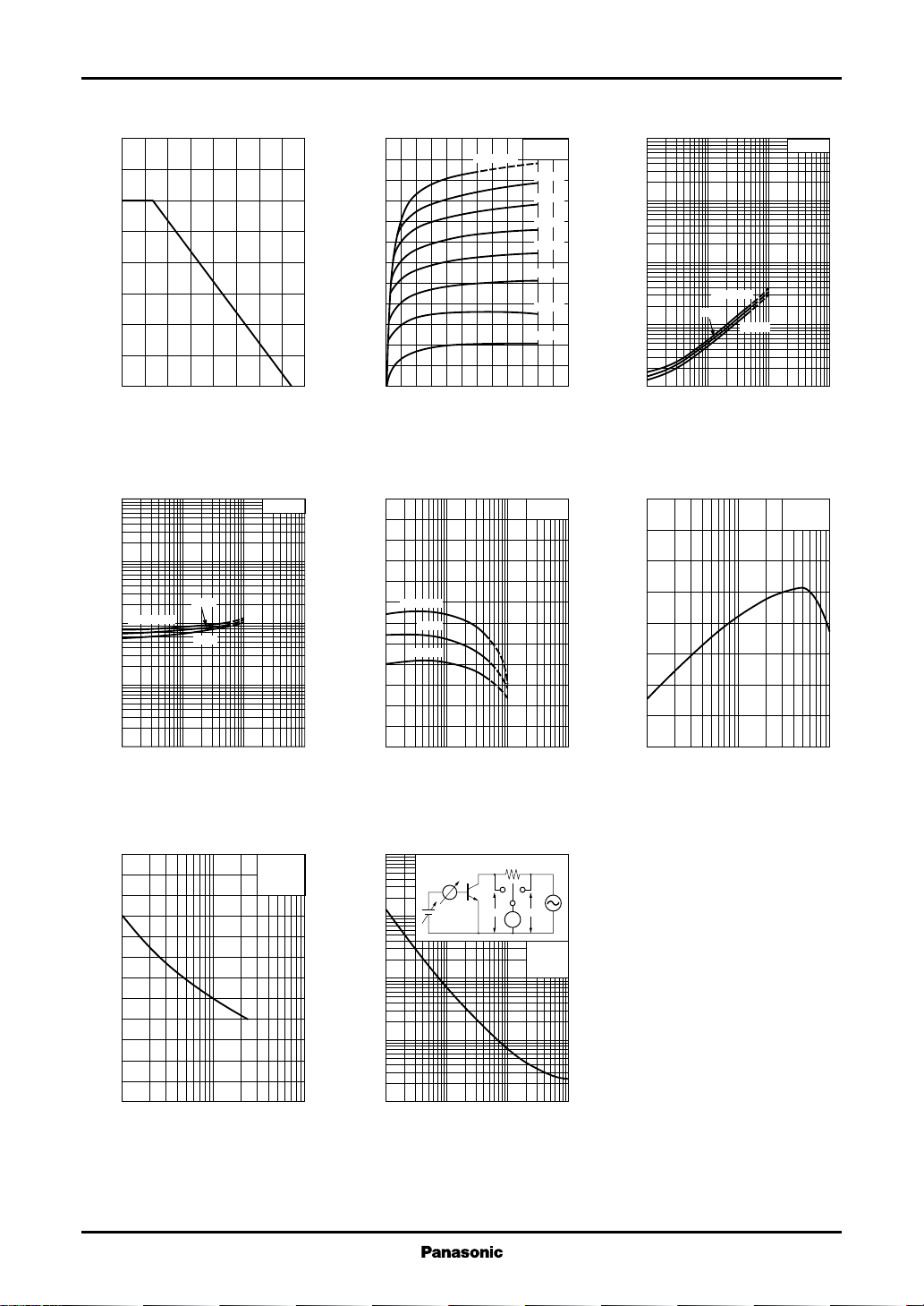
PC — Ta IC — V
800
)
700
mW
(
C
600
500
400
300
200
100
Collector power dissipation P
0
0 16040 12080 14020 10060
Ambient temperature Ta (˚C
V
— I
BE(sat)
100
)
V
(
30
BE(sat)
10
3
Ta=–25˚C
1
0.3
0.1
0.03
Base to emitter saturation voltage V
0.01
0.01 0.1 1 100.03 0.3 3
Collector current IC (A
C
IC/IB=10
25˚C
75˚C
)
V
CE
1.2
1.0
)
A
(
0.8
C
0.6
0.4
Collector current I
0.2
0
0654132
)
Collector to emitter voltage VCE (V
hFE — I
1200
FE
1000
800
Ta=75˚C
600
400
200
Forward current transfer ratio h
25˚C
–25˚C
0
0.01 0.1 1 100.03 0.3 3
Collector current IC (A
IB=4.0mA
C
Ta=25˚C
3.5mA
3.0mA
2.5mA
2.0mA
1.5mA
1.0mA
0.5mA
VCE=2V
)
)
100
V
(
30
CE(sat)
10
3
1
0.3
0.1
0.03
0.01
Collector to emitter saturation voltage V
0.01 0.1 1 100.03 0.3 3
)
Collector current IC (A
400
350
)
MHz
300
(
T
250
200
150
100
Transition frequency f
50
0
–1 –3 –10 –30 –100
Emitter current IE (mA
CE(sat)
Ta=75˚C
25˚C
fT — I
— I
–25˚C
E
C
IC/IB=25
)
VCB=10V
Ta=25˚C
)
Cob — V
24
)
pF
(
20
ob
16
12
8
4
CB
Collector output capacitance C
0
1 3 10 30 100
Collector to base voltage VCB (V
2
IE=0
Ta=25˚C
f=1MHz
)
Ron — I
1000
300
)
100
Ω
(
on
ON resistance R
Ron measuring circuit
=1mA
I
B
30
10
3
1
0.3
0.1
0.01 0.1 1 100.03 0.3 3
Base current IB (mA
B
V
V
B
A
V
f=1kHz
V=0.3V
)
 Loading...