

Panasonic 2SD1280 Datasheet
Transistor
2SD1280
Silicon NPN epitaxial planer type
For low-voltage type medium output power amplification
Features
■
●
Low collector to emitter saturation voltage V
●
Satisfactory operation performances at high efficiency with the
low-voltage power supply.
●
Mini Power type package, allowing do wnsizing of the equipment
and automatic insertion through the tape packing and the magazine packing.
Absolute Maximum Ratings (Ta=25˚C)
■
Parameter
Collector to base voltage
Collector to emitter voltage
Emitter to base voltage
Peak collector current
Collector current
Collector power dissipation
Junction temperature
Storage temperature
*
Printed circuit board: Copper foil area of 1cm2 or more, and the board
thickness of 1.7mm for the collector portion
Symbol
V
CBO
V
CEO
V
EBO
I
CP
I
C
*
P
C
T
j
T
stg
Ratings
20
20
150
–55 ~ +150
5
2
1
1
CE(sat)
.
Unit
V
V
V
A
A
W
˚C
˚C
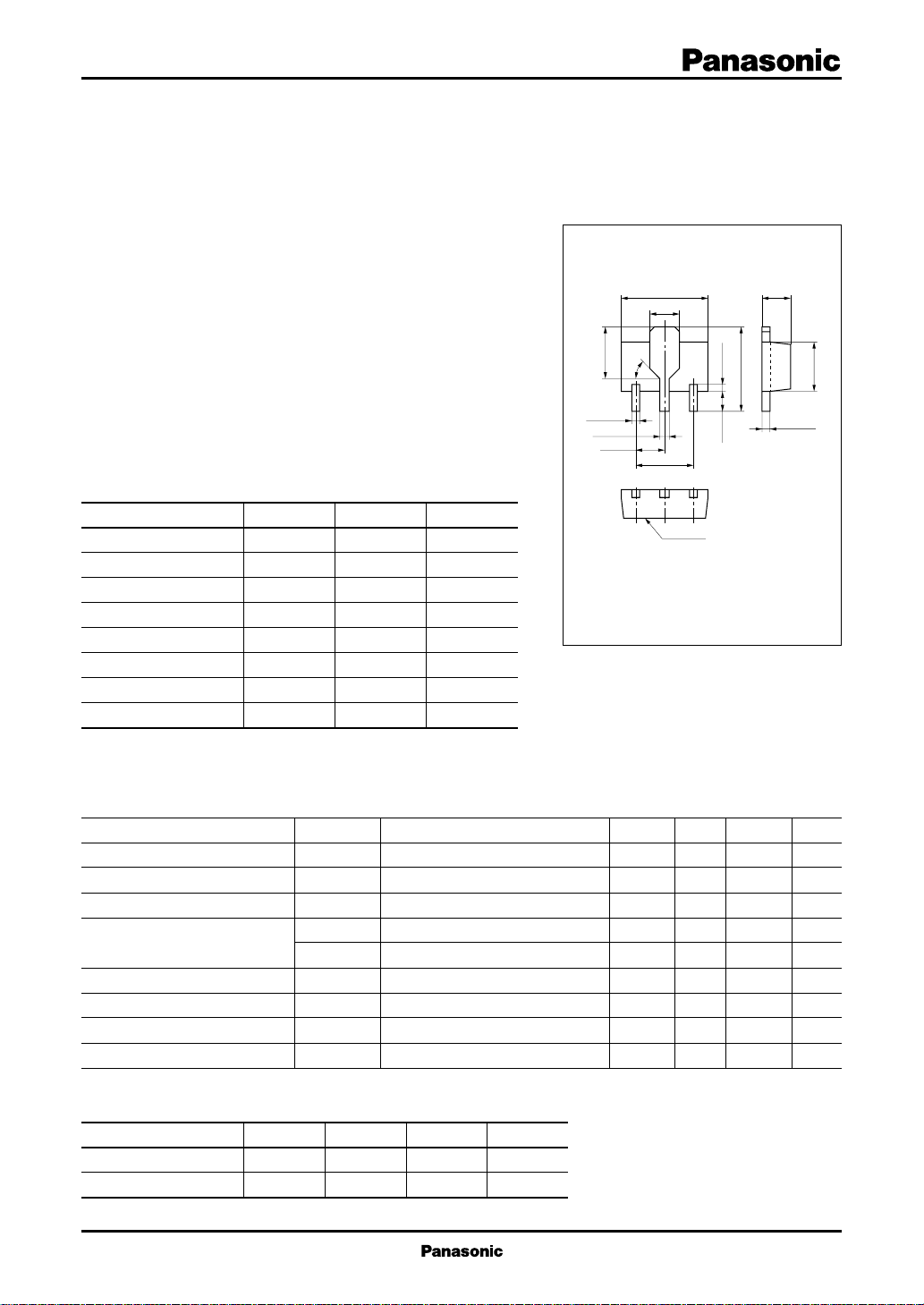
4.5±0.1
1.6±0.2
2.6±0.1
45°
0.4±0.08
0.5±0.08
1.5±0.1
3.0±0.15
321
marking
1:Base
2:Collector EIAJ:SC–62
3:Emitter Mini Power Type Package
1.5±0.1
–0.20
+0.25
0.4max.1.0
4.0
–0.2
+0.1
Marking symbol : R
Unit: mm
2.5±0.1
0.4±0.04
Electrical Characteristics (Ta=25˚C)
■
Parameter
Collector cutoff current
Collector to emitter voltage
Emitter to base voltage
Forward current transfer ratio
Base to emitter saturation voltage
Collector to emitter saturation voltage
Transition frequency
Collector output capacitance
*1
h
Rank classification
FE1
Symbol
I
CBO
V
CEO
V
EBO
*1
h
FE1
h
FE2
V
BE(sat)
V
CE(sat)
f
T
C
ob
VCB = 10V, IE = 0
IC = 1mA, IB = 0
IE = 10µA, IC = 0
VCE = 2V, IC = 500mA
VCE = 2V, IC = 1.5A
IC = 500mA, IB = 50mA
IC = 1A, IB = 50mA
VCB = 6V, IE = –50mA, f = 200MHz
VCB = 6V, IE = 0, f = 1MHz
Rank Q R S T
h
FE1
90 ~ 155 130 ~ 210 180 ~ 280 250 ~ 360
Marking Symbol RQ RR RS RT
Conditions
*2
*2
min
20
*2
90
50
*2
typ
max
1
Unit
µA
V
5
150
360
V
100
1.2
0.5
150
18
*2
Pulse measurement
V
V
MHz
pF
1
Transistor
2SD1280
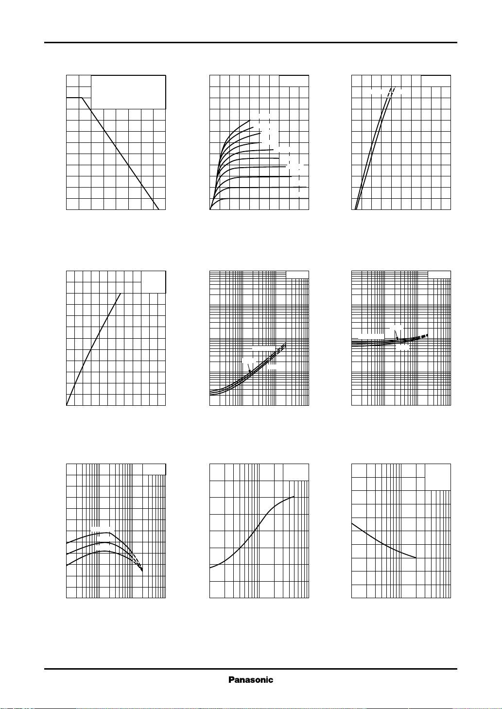
PC — Ta IC — V
1.2
)
W
(
1.0
C
0.8
0.6
0.4
0.2
Collector power dissipation P
0
1.2
1.0
)
A
(
0.8
C
0.6
0.4
Collector current I
0.2
0
Printed circut board: Copper
foil area of 1cm
the board thickness of 1.7mm
for the collector portion.
0 16040 12080 14020 10060
2
or more, and
Ambient temperature Ta (˚C
IC — I
B
012108264
Base current IB (mA
VCE=2V
Ta=25˚C
)
CE
1.2
1.0
)
A
(
0.8
C
0.6
0.4
IB=5.0mA
Collector current I
0.2
0
0 2.01.60.4 1.20.8
)
Collector to emitter voltage VCE (V
V
CE(sat)
)
100
V
(
30
CE(sat)
10
3
1
0.3
0.1
0.03
0.01
Collector to emitter saturation voltage V
0.01 0.1 1 100.03 0.3 3
Ta=75˚C
25˚C
Collector current IC (A
4.5mA
4.0mA
3.5mA
— I
–25˚C
3.0mA
2.5mA
C
Ta=25˚C
2.0mA
1.5mA
1.0mA
0.5mA
IC/IB=20
)
1.2
1.0
)
A
(
0.8
C
0.6
0.4
Collector current I
0.2
)
Collector to emitter saturation voltage V
100
)
V
(
30
BE(sat)
10
0.3
0.1
0.03
Base to emitter saturation voltage V
0.01
IC — V
CE(sat)
Ta=25˚C
IC/IB=10 20
0
00.50.40.1 0.30.2
V
— I
BE(sat)
3
Ta=–25˚C
1
0.01 0.1 1 100.03 0.3 3
C
25˚C
75˚C
Collector current IC (A
CE(sat
IC/IB=10
)
(V
)
)
hFE — I
C
600
FE
500
400
300
200
100
Forward current transfer ratio h
0
0.01 0.1 1 100.03 0.3 3
Ta=75˚C
25˚C
–25˚C
Collector current IC (A
2
fT — I
E
=2V
V
CE
)
200
175
)
MHz
150
(
T
125
100
75
50
Transition frequency f
25
0
–1 –3 –10 –30 –100
Emitter current IE (mA
VCB=6V
Ta=25˚C
)
50
)
pF
(
40
ob
30
20
10
Collector output capacitance C
0
Collector to base voltage VCB (V
Cob — V
1 3 10 30 100
CB
IE=0
f=1MHz
Ta=25˚C
)
 Loading...