

Panasonic 2SD1205A, 2SD1205 Datasheet
Transistor
2SD1205, 2SD1205A
Silicon NPN epitaxial planer type darlington
For low-frequency amplification
Features
■
●
Forward current transfer ratio hFE is designed high, which is appropriate to the driver circuit of motors and printer bammer: h
= 4000 to 2000.
●
A shunt resistor is omitted from the driver.
●
M type package allowing easy automatic and manual insertion as
well as stand-alone fixing to the printed circuit board.
Absolute Maximum Ratings (Ta=25˚C)
■
Parameter
Collector to
base voltage
Collector to
emitter voltage
2SD1205
2SD1205A
2SD1205
2SD1205A
Emitter to base voltage
Peak collector current
Collector current
Collector power dissipation
Junction temperature
Storage temperature
Electrical Characteristics (Ta=25˚C)
■
Parameter
Collector cutoff current
Emitter cutoff current
Collector to base
voltage
Collector to emitter
voltage
Emitter to base voltage
Forward current transfer ratio
Collector to emitter saturation voltage
Base to emitter saturation voltage
Transition frequency
*1
hFE Rank classification
Rank Q R
h
4000 ~ 10000 8000 ~ 20000
FE
Symbol
2SD1205
2SD1205A
2SD1205
2SD1205A
Ratings
V
CBO
V
CEO
V
EBO
I
CP
I
C
P
C
T
j
T
stg
30
60
25
50
5
750
500
400
150
–55 ~ +150
Symbol
I
I
V
V
V
h
V
V
f
CBO
EBO
FE
T
CBO
CEO
EBO
*1
CE(sat)
BE(sat)
VCB = 25V, IE = 0
VEB = 4V, IC = 0
IC = 100µA, IE = 0
IC = 1mA, IB = 0
IE = 100µA, IC = 0
VCE = 10V, IC = 500mA
IC = 500mA, IB = 0.5mA
IC = 500mA, IB = 0.5mA
VCB = 10V, IE = –50mA, f = 200MHz
FE
Unit
V
V
V
mA
mA
mW
˚C
˚C
Conditions
6.9±0.1
1.5
1.5 R0.9
0.4
R0.9
R0.7
1.0±0.1
0.85
0.55±0.1 0.45±0.05
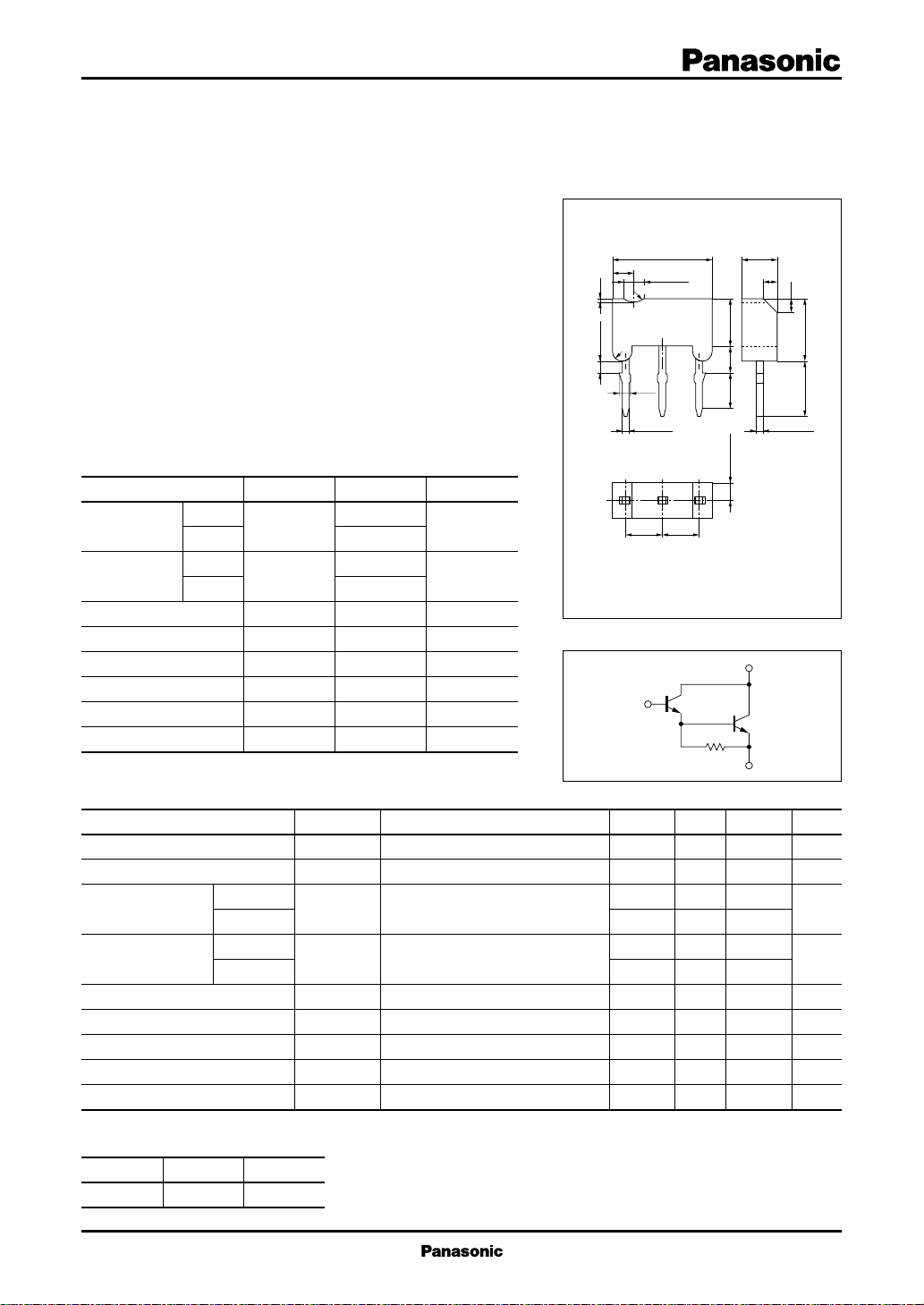
2.5 2.5
1:Base
2:Collector EIAJ:SC–71
3:Emitter M Type Mold Package
Internal Connection
B
min
30
60
25
50
5
*2
*2
*2
4000
2.5±0.1
3.5±0.1
2.0±0.2
2.4±0.21.25±0.05
123
≈200Ω
typ
max
100
100
20000
2.5
150
*2
Pulse measurement
C
E
3
Unit: mm
1.0
1.0
4.1±0.2 4.5±0.1
Unit
nA
nA
V
V
V
V
V
MHz
1
Transistor
2SD1205, 2SD1205A
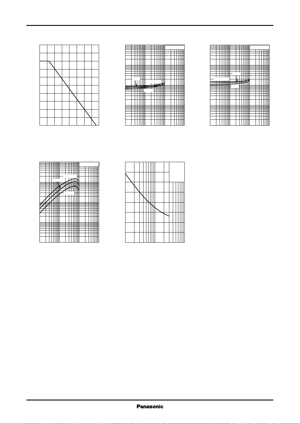
PC — Ta V
500
)
mW
(
400
C
300
200
100
Collector power dissipation P
0
0 16040 12080 14020 10060
Ambient temperature Ta (˚C
hFE — I
C
5
10
FE
4
10
3
10
25˚C
Ta=75˚C
–25˚C
VCE=10V
— I
)
100
V
(
30
CE(sat)
10
3
25˚C
1
0.3
0.1
0.03
0.01
Collector to emitter saturation voltage V
0.01 0.1 1 100.03 0.3 3
)
–25˚C
Collector current IC (A
Cob — V
8
)
pF
7
(
ob
6
5
4
CE(sat)
Ta=75˚C
CB
C
IC/IB=1000
IE=0
f=1MHz
Ta=25˚C
100
)
V
(
30
BE(sat)
10
0.3
0.1
0.03
Base to emitter saturation voltage V
0.01
)
V
— I
BE(sat)
3
Ta=–25˚C
1
0.01 0.1 1 100.03 0.3 3
C
IC/IB=1000
25˚C
75˚C
Collector current IC (A
)
2
10
Forward current transfer ratio h
10
0.01 0.1 1 100.03 0.3 3
Collector current IC (A
3
2
1
Collector output capacitance C
0
1 3 10 30 100
)
Collector to base voltage VCB (V
)
2
 Loading...