

Page 1

®
ChromaCastChromaCast
82C205
LCD Monitor Controller
Preliminary Programmer’s Guide
CONFIDENTIAL
Revision 1.0
915-2000-084
11/22/99
Page 2

Copyright
Copyright © 1999 OPTi Inc. All rights reserved. No part of this publication may be reproduced, transmitted,
transcribed, stored in a retrieval system, or translated into any language or computer language, in any form or by
any means, electronic, mechanical, magnetic, optical, manual, or otherwise, without the prior written permission of
OPTi Inc., 1440 McCarthy Blvd. Milpitas, CA 95035.
Disclaimer
OPTi Inc. makes no representations or warranties with respect to the design and documentation herein described and
especially disclaims any implied warranties of merchantability or fitness for any particular purpose. Further, OPTi Inc.
reserves the right to revise the design and associated documentation and to make changes from time to time in the content
without obligation of OPTi Inc. to notify any person of such revisions or changes.
Trademarks
OPTi and OPTi Inc. are registered trademarks of OPTi Inc. All other trademarks and copyrights are the property
of their respective holders.
OPTi Inc.
1440 McCarthy Blvd.
Milpitas, CA 95035
Tel: (408) 486-8000
Fax: (408) 486-8001WWW:
http://www.opti.com
Page 3

Programmer's Guide
®
ChromaCast 82C205
Table of Contents
INTRODUCTION........................................................................................................................................................1
NOMENCLATURE.....................................................................................................................................................2
CHOOSING CHROMACAST 82C205 HARDWARE CONFIGURATION .................................................................3
CONFIGURING CHROMACAST 82C205 FOR A SPECIFIC PANEL......................................................................3
DISPLAY CRTC PROGRAMMING..............................................................................................................................4
Pixel Clock Frequency (in MHz):...................................................................................................................4
Horizontal Sync Polarity: ...............................................................................................................................4
Horizontal Sync Width (in units of pixel clock)...............................................................................................5
Horizontal Display Start (in units of pixel clock) ............................................................................................5
Horizontal Display End (in units of pixel clock)..............................................................................................5
Horizontal Total (in units of pixel clock).........................................................................................................6
Vertical Sync Polarity.....................................................................................................................................6
Vertical Sync Width (in units of video lines) ..................................................................................................6
Vertical Display Start (in units of video lines)................................................................................................6
Vertical Display End (in units of video lines) .................................................................................................7
Vertical Total (in units of video lines).............................................................................................................7
Panel Window Default Settings.....................................................................................................................7
DISPLAY TIMING WAVEFORMS.................................................................................................................................8
Vertical Timing for TFT Panel........................................................................................................................8
Horizontal Timing for TFT Panel....................................................................................................................9
Detail of Pixel Clock Timing...........................................................................................................................9
VGA VIDEO INPUT INTERFACE ............................................................................................................................11
CALCULATING THE HORIZONTAL SYNC FREQUENCY (F
CALCULATING THE REFRESH RATE OR VERTICAL SYNC FREQUENCY (F
DETERMINING THE RESOLUTION OF THE INCOMING VGA........................................................................................12
DETERMINING THE FREQUENCY OF THE PIXEL CLOCK USED BY THE VGA ...............................................................12
DETERMINING THE POLARITY OF THE HORIZONTAL AND VERTICAL INCOMING SYNCS..................................................12
CAPTURE CRTC PROGRAMMING ..........................................................................................................................12
HORIZONTAL SYNC WIDTH (IN UNITS OF VCLK1)...................................................................................................13
)OF THE INCOMING VGA...............................................11
HSYNC
) OF THE INCOMING VGA.....................11
VSYNC
HORIZONTAL DISPLAY START (IN UNITS OF PIXEL CLOCK)........................................................................................13
HORIZONTAL DISPLAY END (IN UNITS OF PIXEL CLOCK)...........................................................................................13
HORIZONTAL TOTAL (IN UNITS OF PIXEL CLOCK) .....................................................................................................13
915-2000-084 Page iii
Revision 1.0
Page 4

Programmer's Guide
ChromaCast 82C205
VERTICAL SYNC WIDTH (IN UNITS OF VIDEO LINES).................................................................................................13
VERTICAL DISPLAY START (IN UNITS OF VIDEO LINES).............................................................................................14
VERTICAL DISPLAY END (IN UNITS OF VIDEO LINES) ................................................................................................14
VERTICAL TOTAL (IN UNITS OF VIDEO LINES)...........................................................................................................14
PROGRAM THE CAPTURE CRTC TO SYNCHRONIZE TO EXTERNAL SYNCS ...............................................................15
DITHER.....................................................................................................................................................................17
SCALING ..............................................................................................................................................................17
Setting the Input Resolution for the Scaler..................................................................................................17
Setting the Output Resolution......................................................................................................................18
Setting the Scaling Ratios ...........................................................................................................................18
Horizontal Ratio:..........................................................................................................................................19
FINE TUNING THE SCALERS...................................................................................................................................19
USING THE ANTI-ALIAS FILTER..............................................................................................................................20
“CENTERING”.........................................................................................................................................................21
HOW THE DISPLAY WINDOW AFFECTS THE SCALER ...............................................................................................21
SETTING THE PANEL WINDOW REGISTER WITHOUT “CENTERING” ...........................................................................21
CONTRAST AND BRIGHTNESS ADJUSTMENT ..................................................................................................23
DIGITAL CONTRAST ..............................................................................................................................................23
DIGITAL BRIGHTNESS............................................................................................................................................23
THE ON SCREEN DISPLAY....................................................................................................................................25
DETERMINING OSD SIZE......................................................................................................................................25
DETERMINING OSD LOCATION ON SCREEN ...........................................................................................................25
SELECTING OSD ATTRIBUTES ..............................................................................................................................25
ALPHA BLEND OPERATION....................................................................................................................................26
CONTENTS OF THE REGISTER COLOR LOOK-UP TABLE ..........................................................................................26
TRANSFERRING BITMAP FROM CPU ROM TO DISPLAY ..........................................................................................26
MEMORY CONFIGURATION AND ALLOCATION.................................................................................................27
BYPASSING THE MEMORY SUBSYSTEM..................................................................................................................27
CONFIGURING THE DRAM INTERFACE...................................................................................................................27
Selecting DRAM speed................................................................................................................................27
Programming the refresh rate......................................................................................................................28
Specifying the burst length and type, and CAS Latency.............................................................................28
Additional memory configuration settings....................................................................................................28
DRAM BUFFER ALLOCATION................................................................................................................................29
915-2000-084
Revision 1.0 Page iv
®
Page 5

Programmer's Guide
ChromaCast 82C205
Allocating the DRAM space to each buffer..................................................................................................29
VGA Frame Buffer.......................................................................................................................................30
TV Frame Buffers ........................................................................................................................................30
OSD Buffer ..................................................................................................................................................31
Display Read Out from Frame Buffers ........................................................................................................31
CPU Scratch RAM.......................................................................................................................................32
TESTING AND DEBUGGING..................................................................................................................................33
INTERNAL TEST PATTERNS ...................................................................................................................................33
SOFTWARE RESETS AND DISABLES.......................................................................................................................33
REVISION NUMBER...............................................................................................................................................34
FIFO STATUS ......................................................................................................................................................34
SIGNATURE ANALYZERS .......................................................................................................................................34
CPU MEMORY READ BUFFER...............................................................................................................................34
MEMORY SUBSYSTEM STATUS..............................................................................................................................35
MISCELLANEOUS..................................................................................................................................................35
TV MODE SETUP ....................................................................................................................................................37
SELECTING BETWEEN 8-BIT AND 16-BIT TV DECODER INTERFACE ...........................................................................37
DETERMINING IF TV PHASE IS CORRECT ...............................................................................................................37
REQUIRED SYNCHRONIZATION SIGNALS FROM THE TV DECODER............................................................................37
ENABLING TV MODE.............................................................................................................................................37
PROGRAMMING THE CRTC FOR TV MODE............................................................................................................38
PROGRAMMING THE SCALERS FOR TV MODE ........................................................................................................38
IP CONVERSION...................................................................................................................................................38
Bob Mode ....................................................................................................................................................38
CPU INTERFACE.....................................................................................................................................................41
CPU ACCESS TO THE REGISTERS.........................................................................................................................41
CPU ACCESS TO THE DRAM BUFFER ..................................................................................................................41
INTERRUPTS.........................................................................................................................................................42
Enabling an event to generate an interrupt.................................................................................................42
The interrupt/event status register...............................................................................................................42
Clearing an interrupt/event..........................................................................................................................43
POWER MANAGEMENT FOR CHROMACAST 82C205 .......................................................................................45
TIMER..................................................................................................................................................................45
Setting the timer interval..............................................................................................................................45
915-2000-084
Revision 1.0 Page v
®
Page 6

Programmer's Guide
ChromaCast 82C205
Timer Operation Procedure.........................................................................................................................45
POWER SEQUENCING ...........................................................................................................................................45
DPMS POWER MANAGEMENT ..............................................................................................................................46
Notifying the CPU of the DPMS state..........................................................................................................46
Monitor is disconnected from the VGA controller........................................................................................46
ChromaCast 82C205 Power Conservation Techniques..............................................................................46
Example of Power Conservation Policy for DPMS......................................................................................47
APPENDIX A: EXAMPLE REGISTER INITIALIZATION VALUES.........................................................................49
APPENDIX B: COMMON VGA TIMING VALUES...................................................................................................51
APPENDIX C: VCLK2 PLL M & N VALUES...........................................................................................................53
APPENDIX D: CHROMACAST OSD (ON-SCREEN DISPLAY) USER'S GUIDE..................................................57
ENABLING OSD....................................................................................................................................................57
SUPPORTED FUNCTIONS.......................................................................................................................................57
Front Panel input buttons description..........................................................................................................57
RESET .................................................................................................................................................................57
SELECT................................................................................................................................................................57
ADJUST................................................................................................................................................................57
MODE ..................................................................................................................................................................57
RESET BUTTON.....................................................................................................................................................57
MODE BUTTON .....................................................................................................................................................57
DESCRIPTION OF SUPPORTED ICONS.....................................................................................................................58
Contrast Icon: ..............................................................................................................................................58
Brightness Icon:...........................................................................................................................................58
Horizontal position Icon: ..............................................................................................................................58
Horizontal Screen size Icon:........................................................................................................................58
Vertical Position Icon:..................................................................................................................................58
Vertical Screen Size Icon:............................................................................................................................58
Focus Icon:..................................................................................................................................................58
OPTi Icon:....................................................................................................................................................58
Recall Icon:..................................................................................................................................................59
USER Recall mode......................................................................................................................................59
Factory Recall mode....................................................................................................................................59
VGA or TV input Select mode Icon..............................................................................................................59
Exit menu.....................................................................................................................................................59
915-2000-084
Revision 1.0 Page vi
®
Page 7

Programmer's Guide
ChromaCast 82C205
OSD Description Language Select..............................................................................................................59
MANUFACTURE DEBUGGING MODE.........................................................................................................................60
915-2000-084
Revision 1.0 Page vii
®
Page 8

Programmer's Guide
ChromaCast 82C205
915-2000-084
Revision 1.0 Page viii
®
Page 9

Programmer's Guide
®
ChromaCast 82C205
Introduction
This is the programmer’s guide for the ChromaCast 82C205 LCD Monitor Controller. It is an application note for
the ChromaCast 82C205 Databook that contains detailed register descriptions. This guide will walk the
programmer through the various programming sequences necessary in order to build a customized LCD monitor
control application.
The ChromaCast 82C205 Monitor Controller is a controller for LCD Flat Panel Monitors. The 82C205 performs
several functions including:
• clock generation for the display, and memory,
• scaling,
• frame rate conversion,
• television mode support,
• on screen display menu overlay,
• dithering,
• power management.
The 8051 compatible micro-controller interfaces to the ChromaCast 82C205 LCD Monitor Controller and assists
in the configuration process so the 82C205 can be enabled to perform the above functions. The 8051 will be
referred to hereafter as the CPU or micro-controller.
The CPU initializes the registers of the 82C205, enabling the 82C205 to accept different incoming resolutions and
refresh rates, and allows the 82C205 to interface with many different types of flat panels. In addition, the CPU
provides the on-screen display (OSD) bitmap data to the 82C205, as well as the EDID data used in the Display
Data Channel (DDC). The objective of this programmer’s guide is to present a logical description of each major
function of ChromaCast 82C205 and a methodology for programming these functions. Suggested programming
procedures and values will be included.
This guide is divided into the following sections:
q Configuring ChromaCast 82C205 for a Specific Panel
This section details how to configure ChromaCast 82C205 for a particular panel. Issues such as the
number of bits per pixel that the panel supports, number of pixels per clock, panel resolution, and the
timing of the panel synchronization signals are discussed. In order to configure the ChromaCast 82C205
properly, the programmer must have a copy of the panel timing specification.
q VGA Video Input Interface
This section details how to detect the incoming resolution and synchronization timing from the VGA, as
well as how to program the ChromaCast 82C205 to accept the incoming VGA signal.
q Scaling
This section details how to program the ChromaCast 82C205 Scaler. The 82C205 can display the
incoming video at its original resolution, or it can scale the video up or down to match the panel size. The
video can be displayed full scale on the panel, or in a “centered” mode at its original resolution
surrounded by a black border.
q On Screen Display
This section details how to overlay an on screen display on top of the video path. Issues such as size and
location of the OSD, color depth, attributes, and other tradeoffs are discussed.
q Memory Configuration and Allocation
915-2000-084 Page 1
Revision 1.0
Page 10

Programmer's Guide
ChromaCast 82C205
This section details how to program the 82C205 so it can interface with the DRAM. This section also
allocates the DRAM to buffers for use by the ChromaCast 82C205.
q Testing
This section indicates what sort of testing and debug options are available on the ChromaCast 82C205.
q TV Mode
This section details how to operate the TV mode on the 82C205. The ChromaCast 82C205 interfaces
with an NTSC/PAL decoder and accepts YUV 4:2:2 format. ChromaCast 82C205 performs a YUV to RGB
color space transform and then performs interlace-to-progressive (IP) scan conversion. Discussions of
different interlace-to-progressive conversion options are included.
q CPU Interface
This section explains the CPU interface to the ChromaCast 82C205, including addressing for the
registers, and the DRAM buffer. The interrupt sources are also explained.
q Power Management
This section explains how to operate the general purpose timer on the 82C205, as it is an integral part of
the power management system. Power sequencing for power-up and power-down on the panels is
explained, as well as policies for DPMS power management.
q Example Register Values for ChromaCast 82C205
Appendix A offers an snapshot of the register values during operation of the 82C205. The setup is for a
1024x768, 60 Hz panel accepting a 1024x768, 70 Hz VGA input.
q Common VGA Timing Values
Appendix B includes some common VGA Timing values that describe the incoming VGA signal.
q Memory and Display Clock Programming Table
Appendix C includes the programming settings for the internal PLLs for memory clock and display clock
frequencies.
q On-Screen Display (OSD) User's Guide
Appendix D provides a preliminary user's guide for the use of the On-Screen (0SD) to configure
ChromaCast to provide the most satisfactory image.
Nomenclature
Numbers representing different bases will be denoted as follows: A hexadecimal number will be followed by a
lower case “h”, as in A5h. A number without an “h” appended to it will be assumed to be a decimal value.
915-2000-084
Revision 1.0 Page 2
®
Page 11

Programmer's Guide
®
ChromaCast 82C205
Choosing ChromaCast 82C205 Hardware Configuration
ChromaCast 82C205 has a 24-bit digital interface that can be used with a PanelLink or LVDS receiver or external
A/D converters. In addition to an external A/D converter, ChromaCast 82C205 supports external clock sources.
It is recommended that the system uses an external Reference Clock source and shares the Reference Clock
(14.318 MHz) with the CPU system clock.
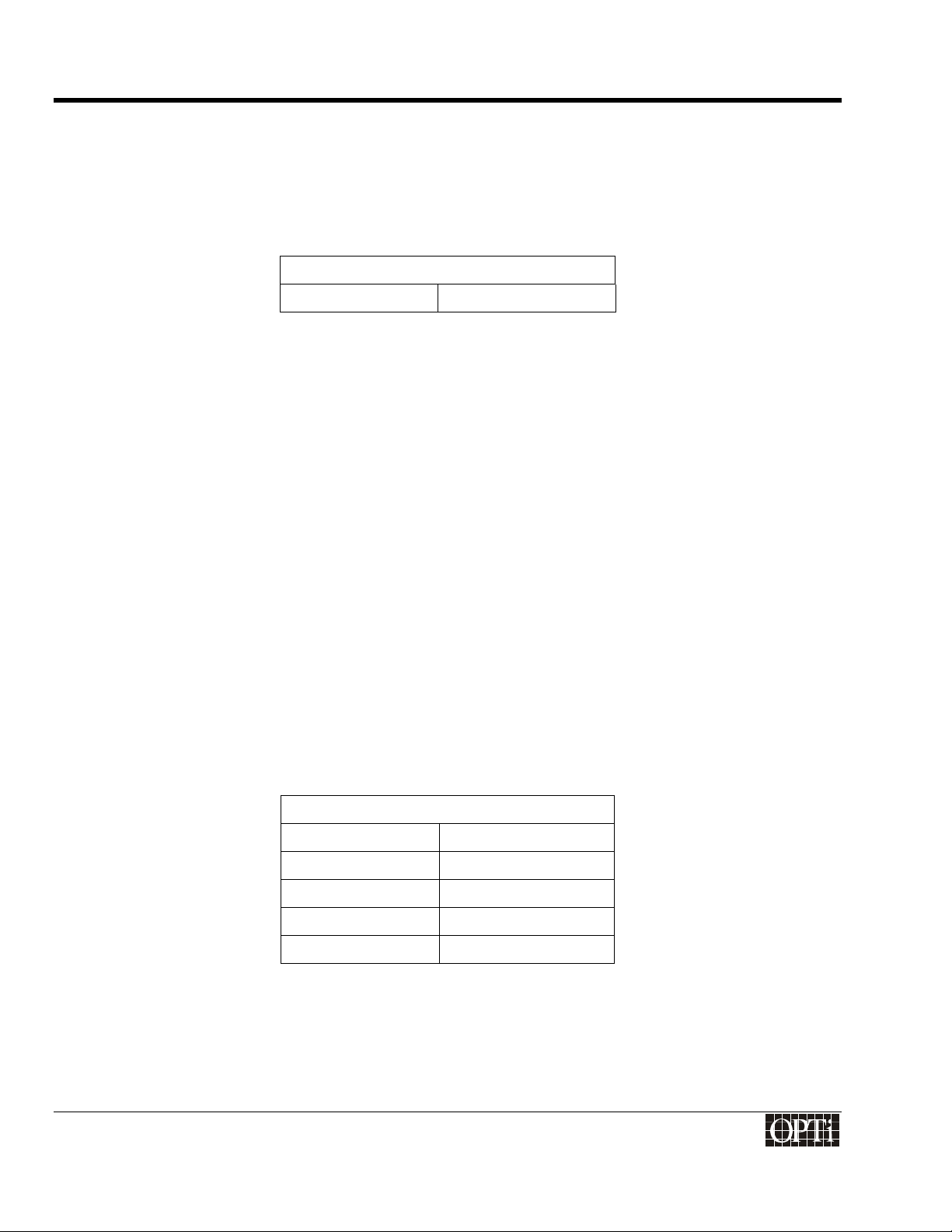
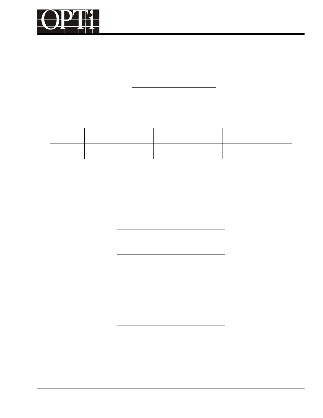
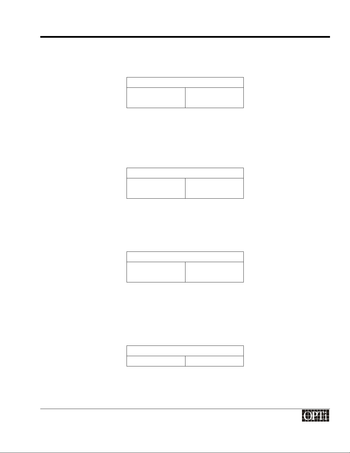
Internal/External Hardware Selection
Internal/External
Memory Clock
Select
Internal/External
Display Clock Select
Register FCh, Bit[3]
Register FCh, Bit[2]
1 = internal clock
0 = external clock
Configuring ChromaCast 82C205 for a Specific Panel
Before beginning, the programmer will need a specification for the panel. The following information should be
extracted from the specification:
• Total Number of Data Lines to Panel
• Bits Per Pixel
• Pixels Per Clock
• Power Sequencing Timing
• Timing for the Horizontal and Vertical Syncs, and Display Enable (DE)
ChromaCast 82C205 uses a resistor strap option at power up to specify some of the above parameters. VESA
naming conventions as referenced in FPDI-1 are used. The following naming conventions are used:
• A = Active, i.e. TFT display
• S = Single Scan. STN and TFT displays are single scan.
For instance, a TFT display with 12-bit color and a 24-bit data interface would be referred to as A-444-S24. The
“444” term indicates 4 bits red, 4 bits green, and 4 bits blue. Using this nomenclature, select the panel type that is
applicable and set the strapping resistors appropriately. Refer to the databook for details on the strapping options.
The strapped panel type can be read from a register.
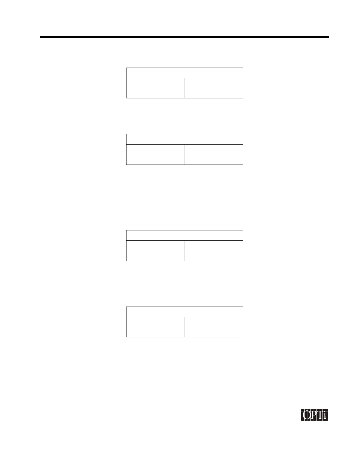
Panel Type
Panel Type
(Read only)
In addition to the strap option, bits per pixel (per color component) must be specified. For example, if the panel
supports 18 bits per pixel (bpp), then the dither “Primary Bits” value should be programmed to 6. (The RGB data
is digitized into 24-bpp values, hence to display 18-bpp, a dithering algorithm must be utilized.) For reasons of
915-2000-084 Page 3
Revision 1.0
Register A0h
Page 12
Programmer's Guide
ChromaCast 82C205
bandwidth or other tradeoffs, the captured data can be also be dithered to a bpp value that is smaller than the
panel supports. The panel drive reformat module will then automatically “scale” the bpp up to the panel
specification. So at the expense of some color depth, an 18 bpp panel could be driven with only 9 bpp captured,
and the 82C205 will automatically format the data to 18 bpp; however, the resultant image will actually only
display 29 colors, instead of the desired 218. There are other dither options, but these will be discussed later. For
very large OSDs or high refresh, high resolution VGA modes, bandwidth can become critical.
Primary Color Bits
Primary Bits Register 38h, Bits[7:4]
Display CRTC Programming
The following parameters for the Display CRTC timing, including pixel clock frequency, horizontal and vertical
sync timings, timing for DE, and polarities of the horizontal and vertical syncs are determined by the specification
for the panel that the ChromaCast 82C205 is controlling.
Pixel Clock Frequency (in MHz):
The panel is driven by a pixel clock, which is the same clock that drives the display subsystem of the ChromaCast
82C205. This pixel clock frequency for a TFT panel is generally between 25 – 108 MHz. This clock can be
generated by an internal PLL within the 82C205 or by an external crystal oscillator. On the panel specification,
this clock is normally called FPSHIFT or FPS. The frequency requirement for this panel must be read from the
panel specification. Call this value FPSF. Then program the VCLK2 PLL so that it outputs the FPSF frequency:
The reference clock for the VCLK2 PLL is 14.318 MHz. Program the N and M values of the PLL (the divider ratio)
so the PLL will generate FPSF frequency. The formula is FPSF = 14.318 MHz * N / M. A table of suggested values
for M and N is included in the Appendix. Unless the display clock needs to be very low frequency, or the duty
cycle needs to be adjusted, the divide by 2 option for the VCLK2 PLL can remain disabled.
One more detail about the pixel clock that needs to be determined is whether or not the clock is gated, i.e. is the
clock continuously toggling, or is it gated so that it is only toggling when data is valid. Most DSTN displays require
a gated clock, while TFT panels do not.
The last pixel clock specification that needs to be programmed is whether the panel data is stable on the falling
edge of pixel clock or the rising edge.
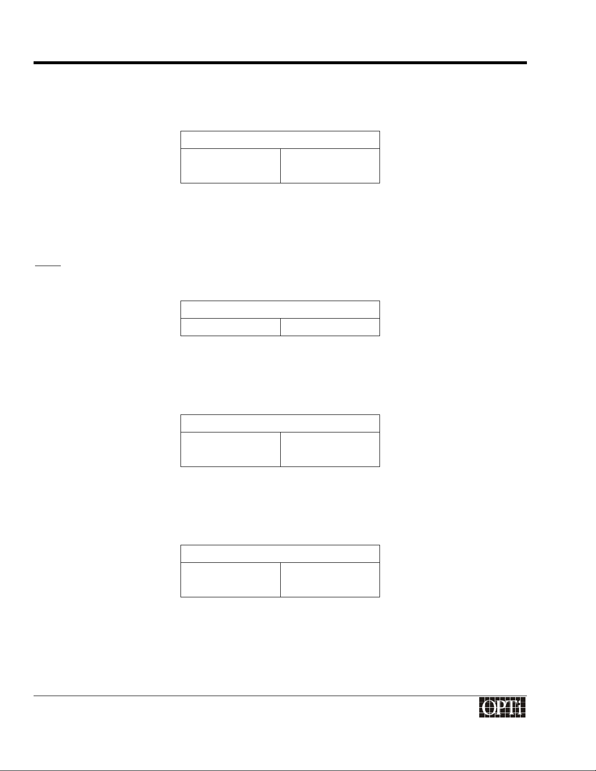
Pixel Clock Frequency
Gated Clock Register A1h, Bit[2]
Clock Phase Register A1h, Bit[3]
Divide Clock by 2 Register C6h, Bit[6]
M Values Register C6h
N Values Register C7h
Horizontal Sync Polarity:
This register sets the polarity of the horizontal sync to the panel. It has no relationship to the polarity of the
incoming sync from the VGA.
915-2000-084
Revision 1.0 Page 4
®
Page 13
Programmer's Guide
ChromaCast 82C205
Note: Polarity can be defined as follows: If the sync is high while data is active, then it is an active low sync. If the
sync is low while data is active, then is it an active high sync.
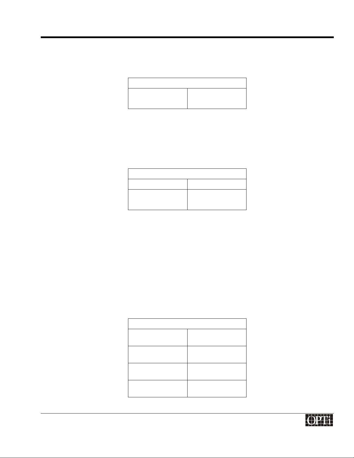
Horizontal Sync Polarity
Polarity Register A1h, Bit[0]
Horizontal Sync Width (in units of pixel clock)
The width of the active part of the sync (when data is not valid).
Horizontal Sync Width
Sync Width Register 82h, 83h
Horizontal Display Start (in units of pixel clock)
This is the time between the start of the horizontal sync and the start of data valid. For TFT displays, special
attention must be given to where the data ready line goes active (DRDY or DE) in order to determine this value.
Hence, this timing specification refers to the time between the start of the horizontal sync and the first pixel clock
following the horizontal sync. The value of the Horizontal Display Start must be an odd number
Horizontal Display Start
Display Start Register 84h, 85h
Horizontal Display End (in units of pixel clock)
This is the time between the start of the horizontal sync and the end of data valid.
Horizontal Display End
Display End Register 86h, 87h
915-2000-084
Revision 1.0 Page 5
®
Page 14
Programmer's Guide
ChromaCast 82C205
Horizontal Total (in units of pixel clock)
This is the period of Horizontal Sync.
Horizontal Total
Total Register 80h, 81h
Vertical Sync Polarity
This register sets the polarity of the vertical sync to the panel. It has no relationship to the polarity of the incoming
sync from the VGA.
Note: Polarity can be defined as follows: If the sync is high while data is active, then it is an active low sync. If the
sync is low while data is active, then it is an active high sync.
Vertical Sync Polarity
Polarity Register A1h, Bit[1]
Vertical Sync Width (in units of video lines)
The width of the active part of the sync (when data is not valid).
Vertical Sync Width
Sync Width Register 8Ch, 8Dh
Vertical Display Start (in units of video lines)
This is the time between the start of the vertical sync and the start of data valid.
Vertical Display Start
Display Start Register 8Eh, 8Fh
915-2000-084
Revision 1.0 Page 6
®
Page 15
Programmer's Guide
ChromaCast 82C205
Vertical Display End (in units of video lines)
This is the time between the start of the vertical sync and the end of data valid.
Vertical Display End
Display End Register 90h, 91h
Vertical Total (in units of video lines)
This is the period of the vertical sync. For ALL panels, if the vertical total value does not differ between even and
odd frames, enter the same value for vertical total in the even vertical total register as in the odd vertical total
register.
Vertical Total
Odd Total Register 88h, 89h
Even Total Register 8Ah, 8Bh
Panel Window Default Settings
Later in this guide the centering option will be discussed, which allows a low resolution image to be displayed on a
higher resolution panel, surrounded by a black border. Until that discussion, assume that the incoming image is
scaled to the full panel size, hence the following Panel Window Registers should be set to the corresponding
values in the Display CRTC as a default.
• Panel Window Horizontal Start = Display CRTC Horizontal Start (Registers 84h, 85h) + 11h
• Panel Window Horizontal End = Display CRTC Horizontal End (Registers 86h, 87h) + 11h
• Panel Window Vertical Start = Display CRTC Vertical Start (Registers 8Eh, 8Fh)
• Panel Window Vertical End = Display CRTC Vertical End (Registers 90h, 91h)
Panel Window Registers
Panel Window
Horizontal Start
Panel Window
Horizontal End
Registers 98h, 99h
Registers 9Ah, 9Bh
Panel Window
Vertical Start
Panel Window
Vertical End
915-2000-084
Revision 1.0 Page 7
Registers 9Ch, 9Dh
Registers 9Eh, 9Fh
®
Page 16
Programmer's Guide
FPFRAME
FPLINE
DE (DRDY)
DATA
ChromaCast 82C205
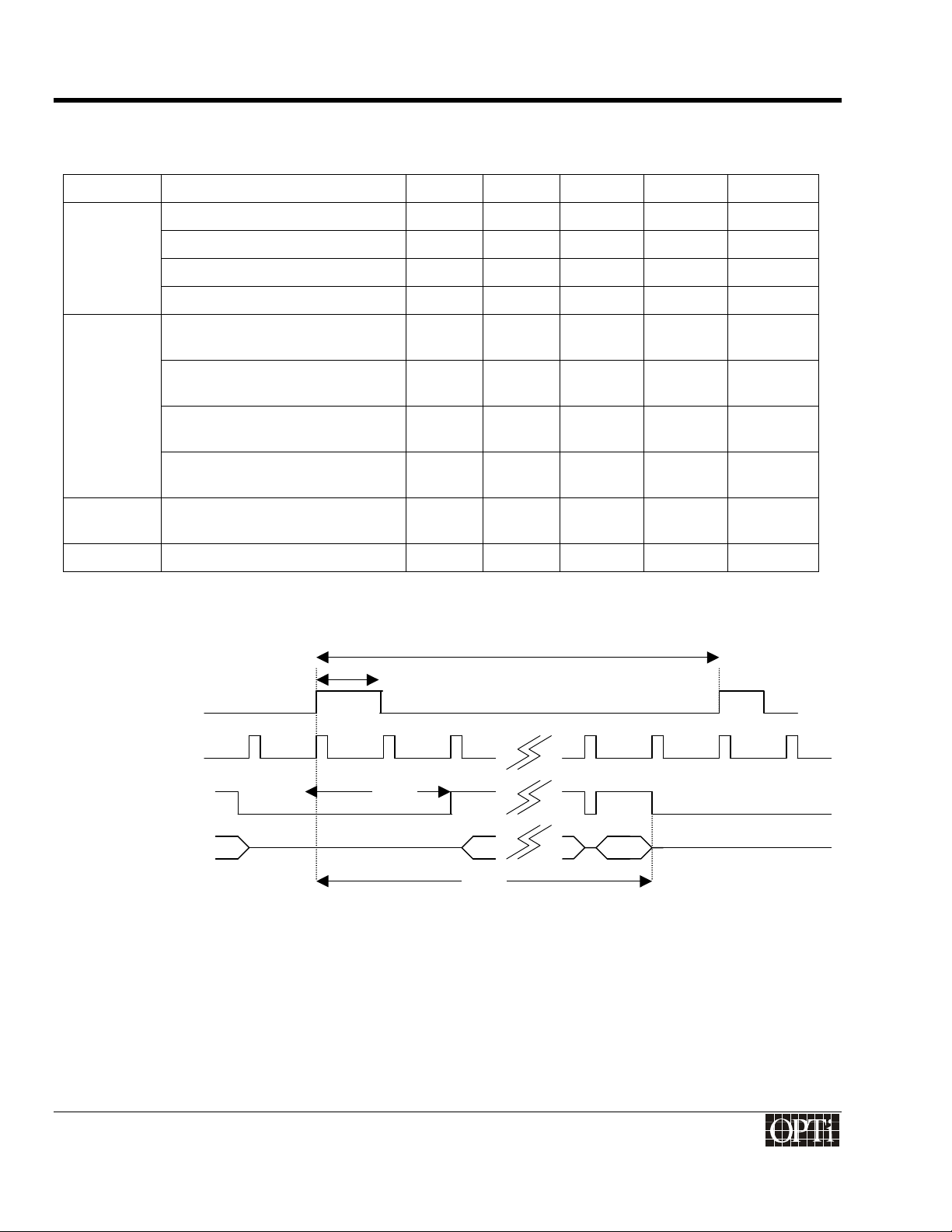
Display Timing Waveforms
Signal Description Symbol Min Typical Max Unit
FPFRAME
Vertical Total t
V Sync Width t
Vertical Display Start t
Vertical Display End t
FPLINE
Horizontal Total t
H Sync Width t
Horizontal Display Start t
Horizontal Display End t
DE Data Valid t
FPSHIFT Pixel Clock Frequency t
Vertical Timing for TFT Panel
t
1
0
1
2
3
5
0 4095 Lines
0 4095 Lines
0 4095 Lines
0 4095 Lines
0 4095 Pixel
Clock
6
0 4095 Pixel
Clock
7
0 4095 Pixel
Clock
8
0 4095 Pixel
Clock
10
0 4095 Pixel
Clock
11
t
0
10 120 MHz
t
2
t
3
915-2000-084
Revision 1.0 Page 8
®
Page 17
Programmer's Guide
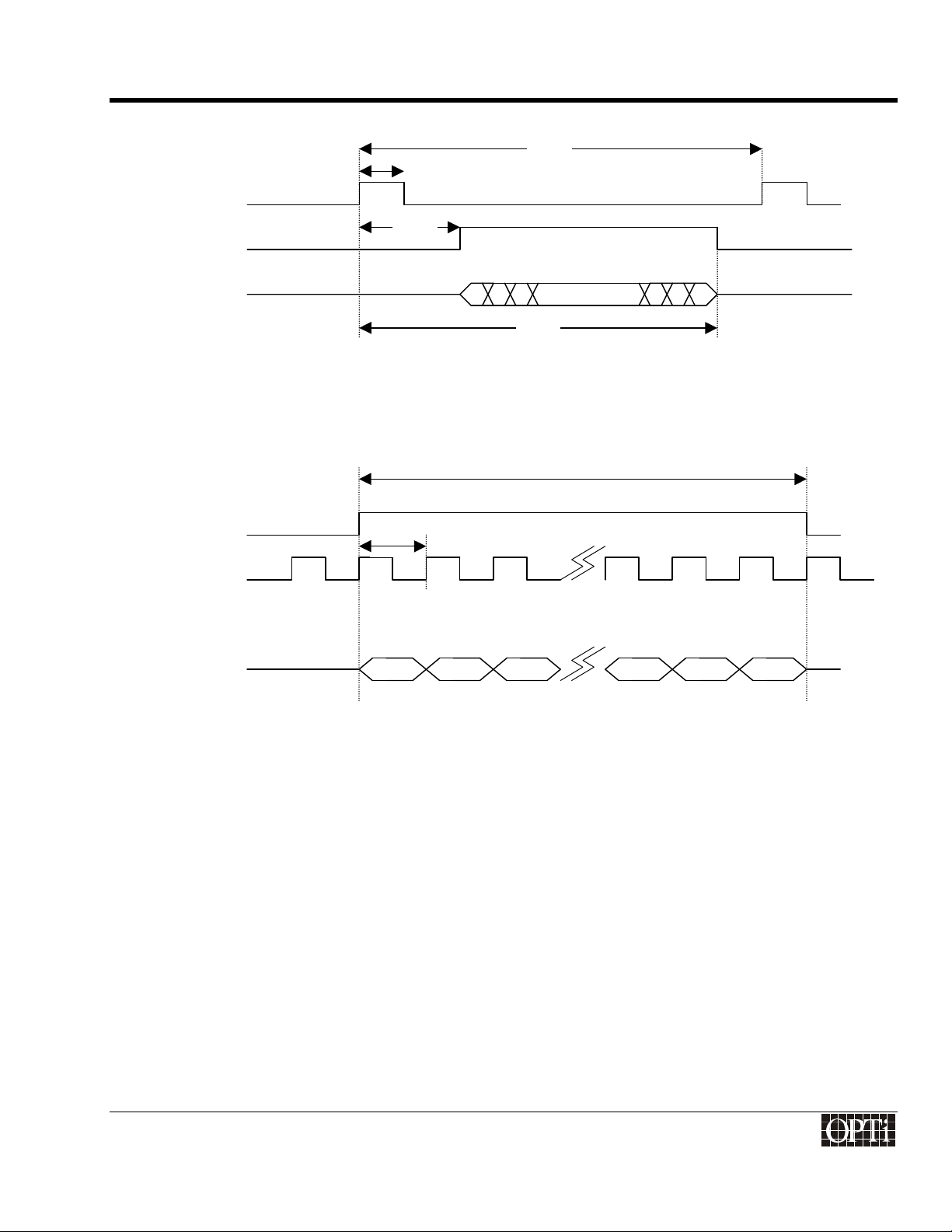
Horizontal Timing for TFT Panel
…
FPLINE
DE (DRDY)
DATA
DE (DRDY)
FPSHIFT
DATA
Detail of Pixel Clock Timing
ChromaCast 82C205
t
t
6
t
7
5
t
8
t
10
t
11
* Polarity of FPFRAME, FPLINE, & FPSHIFT is programmable.
* One and Two Pixels Per Clock are supported.
915-2000-084
®
Revision 1.0 Page 9
Page 18

Programmer's Guide
ChromaCast 82C205
915-2000-084
Revision 1.0 Page 10
®
Page 19
Programmer's Guide
®
ChromaCast 82C205
VGA Video Input Interface
The video data input interface includes a 24-bit digital input port which can be used to interface an external A/D
converter or a PanelLink or LVDS receiver, and an 8/16 bit interface (actually shared with the 24-bit digital input
port) for interfacing to a TV decoder.
Each resolution from the VGA controller has a refresh rate, horizontal sync frequency, and pixel clock frequency
associated with it. The VESA document VESA Monitor Timing Specifications discusses this in depth.
ChromaCast 82C205 provides feedback to the 8051 micro-controller specifying the refresh rate and horizontal
sync frequency of the VGA input. The 8051 micro-controller must then update the capture clock divider word (for
the line-locked PLL), the capture CRTC registers, and the scaler ratio.
Sample VESA Table from VESA Monitor Timing Specifications
Resolution Refresh
Rate
1024x768 60 Hz 48.4 kHz 65 MHz VESA
Horizontal
Frequency
Pixel
Frequency
Standard
Type
Original
Document#
Standard
Date
VG901101A 8/9/91
Guidelines
Calculating the Horizontal Sync Frequency (F
The F
value can be determined by the micro-controller by reading the horizontal sync frequency status
HSYNC
)of the Incoming VGA
HSYNC
register. This register gives the number of reference clock cycles (14.318 MHz or 70 ns) between horizontal sync,
i.e. the period of hsync in units of reference clocks. Then the micro-controller can calculate F
by multiplying
HSYNC
the number of reference clocks * 70 ns and inverting the result:
F
= 1 / (70 ns * number of reference clocks per hsync interval).
HSYNC
Horizontal Sync Frequency Status
Horizontal Sync
Register 72h, 73h
Counter
Calculating the Refresh Rate or Vertical Sync Frequency (F
The F
value can be determined by the micro-controller by reading the resolution counter status register. This
VSYNC
) of the Incoming VGA
VSYNC
register gives the number of horizontal syncs between vertical syncs, i.e. the period of vsync in units of incoming
video lines. Then the micro-controller can calculate F
F
, by the number of horizontal syncs in the vertical interval:
HSYNC
F
VSYNC
= F
/ Resolution counter register value
HSYNC
by dividing the frequency of the horizontal sync,
VSYNC
Vertical Sync Frequency Status
Vertical Sync
Register 70h, 71h
Counter
915-2000-084 Page 11
Revision 1.0
Page 20
Programmer's Guide
ChromaCast 82C205
Determining the Resolution of the Incoming VGA
The resolution of the VGA can be determined by reading the resolution counter status register. This register gives
the number of horizontal syncs between vertical syncs, i.e. the period of vsync in units of incoming video lines.
Then the micro-controller can map this count to the most likely resolution by referencing VESA timing
specifications in the form of a table. For instance, a reading of 810 (decimal) would most likely correspond to 768
active video lines, hence a 1024x768 resolution. The programmer then sets up a quantizer that maps the
resolution counter’s value to the most likely resolution. Blanking time causes the count to be greater than the
number of active lines in a frame, but not significantly greater. Typical resolutions supported are 720x400,
640x480, 800x600, 1024x768, and 1280x1024, but this is a question of policy on how one wishes to define the
quantizer. The resolution counter is the same value used to calculate F
Vertical Sync Frequency Status
VSYNC.
Vertical Sync
Counter
Register 70h, 71h
Determining the frequency of the Pixel Clock used by the VGA
The pixel clock used by the VGA is not transmitted with the data, so it must be determined from the VESA
standards definition. Once the resolution, refresh rate, and horizontal sync frequency are determined, the pixel
clock from the VGA can be calculated by referencing a VESA table. Each resolution has several different refresh
rates, and each rate has a certain recommended pixel clock associated with it. If one wishes to support nonVESA endorsed modes, then that can be accommodated by changing the table mapping.
Determining the polarity of the horizontal and vertical incoming syncs
The 82C205 automatically detects the polarity of the incoming horizontal and vertical syncs from the VGA
controller. The polarities of these incoming syncs are independent of the polarities of the syncs required by the
panel. The incoming sync polarity information is available in a status register.
Capture Sync Polarity Status
Hsync Polarity Register 52h
Bit[2]
Vsync Polarity Register 52h
Bit[3]
Capture CRTC Programming
The Capture CRTC programming is independent of the Display CRTC programming (except in the case of
memory bypass mode where frame rate conversion is not performed). Capture CRTC timing information can be
obtained from reading the above mentioned status registers in the 82C205 and correlating this information with a
VESA Monitor Timing table. The Appendix includes common Capture CRTC settings for certain VGA modes.
915-2000-084
Revision 1.0 Page 12
®
Page 21
Programmer's Guide
ChromaCast 82C205
Horizontal Sync Width (in units of VCLK1)
This register defines the width of the active part of the sync (when data is not valid). This is for internal use, so it
can be set to any value greater that 1. As a rule of thumb, set this to 10.
Horizontal Sync Width
H Sync Width Register 40h, 41h
Horizontal Display Start (in units of pixel clock)
This is the time between the start of the horizontal sync and the start of data valid. It can be calculated by first
looking up the number of pixel clocks between the horizontal sync and the start of active data in the VESA
Computer Monitor Timing Standard. (These values will have to be stored in a table in the CPU program ROM.)
Horizontal Display Start
H Display Start Register 42h, 43h
Horizontal Display End (in units of pixel clock)
This is the time between the start of the horizontal sync and the end of data valid. This is calculated by adding the
horizontal size of the incoming VGA to the Horizontal Display Start value (Registers 42h, 43h).
Horizontal Display End
H Display End Register 44h, 45h
Horizontal Total (in units of pixel clock)
This is the period of Horizontal Sync. This can be determined by reading the Horizontal Frequency Count Register
(Registers 72h, 73h) and performing the following calculation:
Horizontal Total = (Horizontal Frequency Count * VCLK1f / 14.318 MHz) -1
Horizontal Total
H Total Register 46h, 47h
Vertical Sync Width (in units of video lines)
The width of the active part of the sync (when data is not valid). This is for internal use, so it can be set to any
value greater than 1. As a rule of thumb, set this the sync width to 1. The vertical sync width is specified by a start
915-2000-084
Revision 1.0 Page 13
®
Page 22

Programmer's Guide
ChromaCast 82C205
and end value for the Capture CRTC, so in order to achieve a sync width of 1, the sync start should be
programmed to be 1, and the sync end should be programmed to be 2.
Vertical Sync Width
V Sync Start Register 48h
V Sync End Register 4Ah, 4Bh
Vertical Display Start (in units of video lines)
This is the time between the start of the vertical sync and the start of data valid. It can be calculated by first
looking up the number of lines between the vertical sync and the start of active data in the VESA Computer
Monitor Timing Standard. (These values will have to be stored in a table in the CPU program ROM.). See the
Appendix C for some suggested values for Vertical Display Start.
Vertical Display Start
V Display Start Register 4Ch, 4Dh
Vertical Display End (in units of video lines)
This is the time between the start of the vertical sync and the end of data valid. This is calculated by adding the
vertical size of the incoming VGA to the Vertical Display Start value (Registers 4Ch, 4Dh).
Vertical Display End = Vertical Display Start + VGA Vertical Size
Vertical Display End
V Display End Register 4Eh, 4Fh
Vertical Total (in units of video lines)
This is the period of the vertical sync. This value is determined by reading the Resolution Detection register which
indicates the number of lines per Vertical sync (Register 70h, 71h).
915-2000-084
Revision 1.0 Page 14
®
Page 23

Programmer's Guide
ChromaCast 82C205
Vertical Total = Resolution Detection Register Value (Register 70h, 71h)
Vertical Total
V Total Register 50h, 51h
Program the Capture CRTC to Synchronize to External Syncs
The Capture CRTC can be programmed to synchronize to the incoming horizontal and vertical syncs, or it can
free-run by generating its own syncs according to the values in the Capture Horizontal Total and Capture Vertical
Total registers. For normal VGA operation, the CRTC should be synchronized to the external syncs. For internal,
built-in test pattern mode, the CRTC can be programmed to free run.
Capture CRTC Synchronization
Synchronize or Free Run Register 52h, Bits[1:0]
915-2000-084
Revision 1.0 Page 15
®
Page 24

Programmer's Guide
ChromaCast 82C205
915-2000-084
Revision 1.0 Page 16
®
Page 25

Programmer's Guide
®
ChromaCast 82C205
Dither
When the panel requires fewer than 24 bits per pixel (bpp) data, the dither must be enabled. The 24-bit data must
be dithered down to the number of bits that the panel supports. The 24-bit data can also be dithered down to
conserve bandwidth if the system has bandwidth issues. This causes a loss of the number of unique colors that
can be represented, but in many cases, the degradation is not noticeable to the eye.
Earlier, the value for Primary Bits was selected in Register 38h. The dither function then has to be configured
based upon this Primary Bits value. The dither uses an OPTi proprietary algorithm in order to give the user the
perception of true color, even when 24 bits of color are not available to the panel. Due to the proprietary nature of
this algorithm, OPTi provides values and formulas in order to set these registers
1. Set the Dither Frame Depth to 0.
2. Set the Dither Line Depth to (8 - Primary Bits) / 2.
3. Set the Dither Control Register to FAh.
4. Set the Dither Threshold to 0.
5. Set the Dither Algorithm Initializations to 03h.
6. Set the Dither Frame Offset Function Control to 0.
7. Set the Dither Line Offset Function Control to (8 – Primary Bits – Dither Line Depth).
Dither Registers
Primary Bits Register 38h, Bits[7:4]
Dither Frame Select Register 38h, Bits[3:2]
Dither Line Select Register 38h, Bits[1:0]
Dither Control Register 39h
Dither Threshold Register 3Ah
Dither Algorithm
Initialization
Dither Frame Offset Register 3Ch, Bits[7:4]
Dither Line Offset Register 3Ch, Bits[3:0]
Register 3Bh
Scaling
The ChromaCast 82C205 can scale an incoming video signal up to a larger panel resolution, or down to a smaller
panel resolution. The programmer has to specify the incoming resolution, the outgoing resolution, and the scaling
ratios in order for scaling to occur. The scale-down function can be performed without a DRAM frame buffer
(assuming no frame rate conversion), but the scale-up function requires a frame buffer.
Setting the Input Resolution for the Scaler
The incoming image resolution must be specified, whether from TV mode or from the VGA. This incoming
resolution is specified in pixels for the horizontal direction, and in lines for the vertical direction.
915-2000-084 Page 17
Revision 1.0
Page 26

Programmer's Guide
ChromaCast 82C205
VGA Example:
Assuming a 640 x 480 VGA signal, the Xsize = 640 and the Ysize = 480.
When scaling down, add 2Bh to Input Y size (Register 50h, 57h). Assuming a 1280x1024 VGA signal
ouptus to a 1024x768 panel, the Xsize=1280 and the Ysize=1024 + 2Bh.
TV Example:
Assuming a 640 x 240 TV signal (per field), the Xsize = 640 and the Ysize = 240.
Input Resolution for Scaler
Xsize Register 64h, 65h
Ysize Register 56h, 57h
Input Resolution for Scaler
Xsize Register 64h, 65h
Ysize Register 56h, 57h
Setting the Output Resolution
The outgoing resolution of the panel must be specified. The outgoing resolution is specified in pixels for the
horizontal direction, and in lines for the vertical direction.
Assuming a 1024 x 768 VGA signal, the Xsize = 1024 and the Ysize = 768.
Output Resolution for Scaler
Xsize Register 62h, 63h
Ysize Register 58h, 59h
Setting the Scaling Ratios
The horizontal and vertical scaling ratios have to be set separately, and can be determined by the following
formulas.
Vertical Ratio:
• If Scaling Up
Yratio = ((Capture Ysize -1)* 1024) / (Display Ysize. - 1)
• If Scaling Down or no Scaling:
Yratio = (((Display Ysize * 2048) / Capture Ysize) + 1) / 2
915-2000-084
Revision 1.0 Page 18
®
Page 27

Programmer's Guide
Horizontal Ratio:
• Vin Scaler:
If capture Xsize > display Xsize then,
Xratio = (( display Xsize * 8192 ) / ( capture Xsize + 1 )) / 2
Otherwise,
ChromaCast 82C205
Vertical Ratio for Scaler
Yratio Register 54h, 55h
Xratio = 4096
• V
If capture Xsize > display Xsize then,
Otherwise,
The horizontal ratio for the Vout scaler = Register 7Eh, 7Fh.
The VGA Frequency refers to the pixel clock of the incoming VGA signal. The VCLK1 Frequency refers to the
Capture Clock for ChromaCast
Scaler:
out
Xratio = 0
Xratio = (( capture Xsize - 1 ) * 16384 )) / ((display Xsize - 1 ) + 32768 ))
Horizontal Ratio for Vin Scaler
Xratio Register 60h, 61h
Horizontal Ratio for V
Xratio Register 7Eh, 7Fh
Scaler
out
Fine Tuning the Scalers
The following registers need to be set in order to fine tune the scalers. These registers control the Differential
Decision Analyzers (DDA) within the scalers.
1. Set the Vertical Scale-Down Random DDA Initialization to 0001h.
2. Set the Sign Seed Bit to 0h.
3. Set the DDA Field Compensation to 1h.
4. Set the DDA Reference to 1h.
5. Set the Horizontal Scale-Down Random DDA Initialization to 0001h.
Scaler Fine Tune
915-2000-084
Revision 1.0 Page 19
®
Page 28

Programmer's Guide
ChromaCast 82C205
Scaler Fine Tune
Vertical Scale Down
Random DDA Init
Vertical Scale Up
Random DDA Init
Sign Seed Bit Register 5Dh
DDA Field
Compensation
DDA Reference Register 5Eh
Horizontal Scale
Down Random DDA
Init
Register 5Ah, 5Bh
Register 5Ch, 5Dh
Register 5Eh
Register 66h, 67h
Using the Anti-Alias Filter
ChromaCast 82C205 has an anti-alias filter that is used only for scale-down. If the 82C205 needs to scale down,
enable this filter.
Antialias Filter Enable
AntiAlias Enable Register 6Eh
915-2000-084
Revision 1.0 Page 20
®
Page 29

Programmer's Guide
®
ChromaCast 82C205
“Centering”
Up to this point only scaling to the full panel resolution has been discussed. The 82C205 also offers a “centering”
option which allows an image that is of lower resolution than the panel to be displayed in the center of the panel,
surrounded by a black border that makes up the difference between the image resolution and the panel
resolution. This feature is available for panels that support the DE only timing, i.e. horizontal and vertical syncs
are not required.
The Display CRTC is programmed normally, then the Panel Window is programmed. By default, the panel
window should be set to the same values as the corresponding values in the Display CRTC. However, when the
programmer wants the black border to appear, the Panel Window registers should be programmed to reflect the
portion of the display that should actually be displayed. The remainder will be filled in with a black border.
The panel window horizontal start and end registers are in units of VCLK2. The panel window vertical start and
end registers are in units of display horizontal lines.
How the Display Window Affects the Scaler
The window programming must work closely with the scaler, because the display window dimensions become the
virtual panel size for the scaler. The scaler must scale up (or down) to the size of the panel window instead of the
actual panel.
Setting the Panel Window Register without “Centering”
If the 82C205 is not centering, set the Panel Window Registers as follows:
1. Panel Window Horizontal Start = Display CRTC Horizontal Start (Registers 84h, 85h) + 11h
2. Panel Window Horizontal End = Display CRTC Horizontal End (Registers 86h, 87h) + 11h
3. Panel Window Vertical Start = Display CRTC Vertical Start (Registers 8Eh, 8Fh)
4. Panel Window Vertical End = Display CRTC Vertical End (Registers 90h, 91h)
Panel Window Registers
Panel Window
Horizontal Start
Panel Window
Horizontal End
Panel Window
Vertical Start
Panel Window
Vertical End
Registers 98h, 99h
Registers 9Ah, 9Bh
Registers 9Ch, 9Dh
Registers 9Eh, 9Fh
915-2000-084 Page 21
Revision 1.0
Page 30

Programmer's Guide
ChromaCast 82C205
915-2000-084
Revision 1.0 Page 22
®
Page 31

Programmer's Guide
®
ChromaCast 82C205
Contrast and Brightness Adjustment
There are two ways to change the contrast of the image. The first is through the analog gain adjustment on the
external A/D converters. Usually this is adjusted once and then left alone. When the user adjusts the contrast and
brightness through the user interface, the user will adjust the digital contrast and brightness levels.
Digital Contrast
The digital contrast can be adjusted through the following registers. The contrast level can vary from 0 to 255.
Unity gain is represented by the value of 128 (80h).
Digital Contrast
Red Channel Register 68h
Green Channel Register 69h
Blue Channel Register 6Ah
Digital Brightness
The digital brightness can be adjusted through the following registers. The brightness level can vary from -128 to
127. A brightness adjustment value less than 0 will result in a displayed image that is darker than the original
image. A brightness adjustment value greater than 0 will result in a displayed image that is lighter than the original
image. If no adjustment to the image brightness is required, the brightness adjustment should be set to 0.
Digital Brightness Adjustment
Red Channel Register 6Bh
Green Channel Register 6Ch
Blue Channel Register 6Dh
915-2000-084 Page 23
Revision 1.0
Page 32

Programmer's Guide
ChromaCast 82C205
915-2000-084
Revision 1.0 Page 24
®
Page 33

Programmer's Guide
®
ChromaCast 82C205
The On Screen Display
The on screen display is bitmapped based in order to offer flexibility to support fonts of different languages, such
as Chinese and Japanese. Company icons can also be displayed in order to give the OSD a custom feel. Some
issues to decide when designing the OSD are:
Determining OSD Size
The OSD size is programmable and can be as large as the whole screen or as small as a pixel. Even though the
OSD region is rectangular, pixels within the rectangular region can be given transparent attributes to generate the
appearance of a curved edge or any other shaped edge that is desired. One consideration in selecting the size of
the OSD, however, is bandwidth. The larger the OSD, the more bandwidth of will be occupied. The horizontal size
of the OSD is specified in units of pixels (after scaling). The vertical size of the OSD is in units of video lines.
OSD Size
Horizontal Register 2Ch, 2Dh
Vertical Register 30h, 31h
Determining OSD Location on Screen
The OSD, which is a rectangular region, can be located anywhere on the display.
OSD Location
Horizontal Register 2Ah, 2Bh
Vertical Register 2Eh, 2Fh
Selecting OSD Attributes
ChromaCast 82C205 is full of useful attributes for the OSD, such as:
• transparent pixels – opt for a non-rectangular OSD shape
• blinking pixels - the 82C205 can blink to the underlying video, or to the color value in Index 0 of the
register CLUT. The blink rate is programmable; for example, if this value is programmed 30 (decimal), the
pixel will blink on for 30 capture frames, and off for 30 capture frames.
OSD Blinking Configuration
Blink Background Select Register 29h, Bit[2]
Blink Rate Register 32h
915-2000-084 Page 25
Revision 1.0
Page 34

Programmer's Guide
ChromaCast 82C205
• inverted video - use the inverted video as the OSD background so it always stands out from the
underlying display
• translucent pixels - with a programmable blend factor so the user can faintly “see” the underlying video
through the OSD. Never have to worry about the OSD blocking the cursor again. Also one can choose to
have one global blend value for all pixels that the OSD required to be translucent (by using the Register
CLUT).
Alpha Blend Operation
The alpha blend value in ChromaCast 82C205 is 5-bits wide. When the alpha blend value is set to 10h, the OSD
overlay completely obscures the underlying video (this is full scale). When the alpha blend value is set to 00h, the
OSD pixel is transparent. Values between 00h and 10h result in a translucent effect, the result of which is
described by the following formula:
Output = Video * (1-α) + OSD * (α).
Contents of the Register Color Look-Up Table
The Register color look-up table (CLUT) contains 16 entries. Only nibble mode can be for this implementation.
Each entry contains a 3-bit color value (1-bit R,G,B), an alpha blend enable bit, and a 2-bit attribute value for a
total of 6-bits. The two bit attribute value specifies normal, transparent, blinking, or video inversion. If enabling the
alpha blend for a particular index, the global alpha blend value (from a register) is used. All indices with alpha
blending use the same alpha value.
Register CLUT Programming
Global Alpha Blend CFh, Bits[4:0]
CLUT Index 0-F Registers D0h – DFh
Transferring Bitmap from CPU ROM to Display
So now that everything is configured, the programmer needs to generate a bitmap of indices that maps to the
CLUT values stored in ChromaCast 82C205. Just write this bitmap to the OSD DRAM Buffer which is set up and
explained in the Frame Buffer Allocation Section and whenever the programmers wants the OSD on the screen,
enable it with the OSD Enable Register.
OSD Enable Register
Enable OSD Register 29h, Bit[1]
915-2000-084
Revision 1.0 Page 26
®
Page 35

Programmer's Guide
®
ChromaCast 82C205
Memory Configuration and Allocation
The ChromaCast 82C205 uses a 4 Mbyte DRAM buffer for a FRC (Frame Rate Conversion) frame buffer, as well
as a buffer for the OSD bitmap. Frame Rate Conversion means that the 82C205 can accept video arriving at
different refresh rates than the panel supports. The video capture systems will capture at the incoming video rate,
and the display subsystem will read at the outgoing panel rate. If the system doesn’t have to support FRC, then
the system will be limited to supporting only the refresh rate specified by the panel. If the system does not need
FRC and uses an external OSD alternative, the programmer will not need to program the memory subsystem
beyond putting the 82C205 into memory bypass mode. If the system is not bypassing the memory subsystem,
then the programmer will then need to configure the DRAM interface and allocate the frame buffer space.
Bypassing the Memory Subsystem
A single register controls whether the memory subsystem will be bypassed. If the memory is bypassed, however,
the Display CRTC needs to be programmed to synchronize with the Capture CRTC. An offset value for the
vertical sync can also be programmed. This allows the Display Vertical Sync to synchronize to the Capture
Vertical sync, but it will be generated X number of lines after the Capture Vertical Sync. A typical value for this is
5h.
Bypass Memory
Bypass Register A4h
Synchronize Display CRTC to
Capture CRTC
Offset of Display Vertical Sync
from Capture Vertical Sync
Register 97h
Register 92h, 93h
Configuring the DRAM Interface
Selecting DRAM speed
Program the Memory Clock Internal PLL to operate at the DRAM speed. For SDRAM, the typical speed is 100
MHz. The Memory Clock Internal PLL uses a 14.318 MHz clock as its reference. It then uses programmable M
and N values that are configuration registers used to generate higher frequency clocks. Program the M and N
values according to the following formula:
Output Frequency for Memory Clock = 14.318 MHz * N / M
There is a divide by 2 option for the Memory Clock, but it is unlikely to be used. The divide by 2 option will divide
the frequency of the Memory Clock output from the PLL by 2. The ChromaCast 82C205 also provides the option
of not using the internal PLL if it is desired to provide the 82C205 with an external memory clock.
For a 100 MHz memory clock, program the M value to 0Fh and the N value to 69h. The divide by 2 option does
not need to be exercised. The clock also passes through a programmable delay line on its way to the DRAM. This
can be tweaked to obtain better performance. A typical value for the delay line when using the internal PLL is 08h.
When using the external PLL, a typical value for the delay line is 0Eh. The delay line has an intrinsic delay of 0.6
– 0.7 ns (when the delay register is set to 00h), and each increment of the delay line register adds 0.3 – 0.4 ns.
915-2000-084 Page 27
Revision 1.0
Page 36

Programmer's Guide
ChromaCast 82C205
Memory Clock
Delay Line Register 23h
Internal PLL Selection Register FCh, Bit[[3]
Divide by 2 Register C4h, Bit[6][
N Register C5h
M Register C4h
Now the programmer needs to get some information from the DRAM specifications, such as refresh rate for the
DRAM, burst type, and burst length.
Programming the refresh rate
The refresh rate for DRAM is controlled by a counter inside of ChromaCast 82C205. The counter can be
programmed and is clocked by a 14.318 MHz reference clock. Whenever the counter reaches the programmed
terminal count, a refresh request will be generated. Program this rate to 1/3 of the value needed. For example, if
the minimum refresh interval is 10 µs, (which is 10 µs * 14.318 MHz which equals 143.180 reference clocks),
then program the refresh rate to be 143.180 ÷ 3 = 47.730, or in hexadecimal 002Fh.
Refresh Rate
Refresh Rate Register 1Eh, 1Fh
Specifying the burst length and type, and CAS Latency
Interleaved and sequential burst types are supported. Only burst lengths of 8 are supported. CAS latencies of 2
and 3 memory clock cycles are supported. Register 22h, Bits[1:0] must be set to 1's.
SDRAM Control
CAS Latency Register 22h, Bit[3]
Burst Type Register 22h, Bit[2]
Burst Length Register 22h, Bit[1:0]
Additional memory configuration settings
There is a register in 82C205 called “Arbiter Client Acknowledge Overlap”. This bit should be set to “1” in order to
achieve maximum performance.
Optimizing the Memory Subsystem
Arbiter Overlap Register 1Dh, Bit[5]
915-2000-084
Revision 1.0 Page 28
®
Page 37

Programmer's Guide
DRAM Buffer Allocation
ChromaCast 82C205
Now the DRAM interface is configured, and the next step is to allocate the DRAM address space to the various
buffers.
DRAM Buffer Allocation
The frame buffer is used to capture data, and then display it. When the 82C205 is in bypass mode, the frame
buffer is not used. The frame buffer size will vary depending on the application. The larger resolution the display,
the bigger the frame buffer that will be needed.
4 MB
OSD Buffer
Frame Buffer
(VGA or
TV Field 1)
TV Field 2 Buffer
Video
Scratch Pad
CPU Scratch Area
Allocating the DRAM space to each buffer
Each buffer is defined by a start address and pitch. Pitch is the address difference between the start of two
adjacent horizontal lines. An end address is not specified, so the programmer has to keep track of where each
buffer ends, so the next buffer’s start address doesn’t collide with the end of the previous buffer. The end address
is determined by the start address plus the size of the buffer. The start addresses must be on 64*8 boundaries,
i.e., the lowest 9 bits of the 22-bit start address must be all zero. Also, care must be taken to insure that the
buffers do not overlap each other. The pitch should be programmed to the minimum amount of memory required
by a line of that buffer, but it also has the restriction of being on a 64*8 boundary. For instance, if the programmer
was programming the pitch for the OSD buffer, assuming a 300x200 OSD using nibble mode, the pitch should be
programmed to be:
OSD Pitch (in bytes) = [(300 x 4)+(64*8)-1)] / 8
915-2000-084
Revision 1.0 Page 29
®
Page 38

Programmer's Guide
ChromaCast 82C205
which is the number of pixels per lines to be accessed multiplied by the bits per pixel and divided by the word size
which is 64*8 for the DRAM configuration.
VGA Frame Buffer
Calculating the pitch of the frame buffer
The pitch of the frame buffer can be calculated as follows:
Video Pitch (bytes) = {[{VGA Horizontal Size
* Primary Bits
[in pixels]
Register 38h
* 3} + ((64*8)-1)] / 8
The pitch should be chosen to accommodate all the pixels captured in a horizontal line (after scale down) within a
64*8 boundary.
Calculating the size of the frame buffer
The size of the frame buffer is calculated as follows:
Frame Buffer Size (in bytes) = Video Pitch * (the incoming Vertical Size
[in lines]
)
VGA Frame Buffer Start/Pitch
Start Address for Capture (for Frame
Register 04h, 05h, 06h
Buffer or TV Mode Field 1)
Pitch for Capture and Display Buffers
Registers 16h, 17h
(Video Pitch)
TV Frame Buffers
TV mode uses double buffering for the frame buffer, capturing one field in each buffer. Each stored field is 240
lines, so the size of each buffer is 240 lines * the video pitch. In TV mode there are effectively 2 frame buffers,
and in VGA mode only 1 frame buffer.
TV Buffer Size (per field, in bytes) = ( Video Pitch * 240
[lines]
)
The TV Buffer space can be shared with the frame buffer space because VGA and TV are not active at the same
time.
TV Buffer Start/Pitch
Start Address for Capture (for Frame
Register 04h, 05h, 06h
Buffer or TV Mode Field 1)
Start Address for TV Mode Field 2
Registers 07h, 08h, 09h
Capture
Pitch for Capture and Display Buffers
Registers 16h, 17h
(Video Pitch)
915-2000-084
Revision 1.0 Page 30
®
Page 39

Programmer's Guide
ChromaCast 82C205
OSD Buffer
Calculating the OSD Pitch
The pitch of the OSD buffer can be calculated as follows:
OSD Pitch (in bytes) = [(OSD Horizontal Size x 4)+((64*8)-1)] / 8
Calculating the size of the OSD DRAM buffer
The pitch of the OSD determines the size of the OSD buffer required. The OSD DRAM buffer size can be
calculated as follows:
OSD Buffer Size (in bytes) = OSD Pitch * OSD Vertical Size
OSD Buffer Start/Pitch
Start Address for OSD Buffer Registers 0Dh, 0Eh, 0Fh
Pitch for OSD Register 1Ah, 1Bh
OSD FIFO Word Count
This value indicates how many DRAM read accesses that the FIFO will perform in one line. Use the following
formula:
OSD Bandwidth Limit Value = (OSD Horizontal Size * 4) + ((64*8)-1)) / (64*8)
OSD FIFO Word Count
FIFO Word Count Registers B0h
Display Read Out from Frame Buffers
Configuring the display buffers
There are two display buffers, one main one for the normal frame buffer, and one for the second field for TV
mode. The display buffers start addresses should be programmed to match the capture buffer start addresses.
The pitch for the display buffer is set to equal the pitch for the capture buffer, and is shared with the capture pitch
(the register designated Video Pitch).
Display Buffer Setup
Display Panel Start
Address –Field 1
Display Panel Start
Address for TV Mode
Field 2 Capture
Register 10h, 11h, 12h
Registers 13h, 14h, 15h
915-2000-084
Revision 1.0 Page 31
®
Page 40

Programmer's Guide
ChromaCast 82C205
Display FIFO Word Count
This value indicates how many DRAM read accesses that the FIFO will perform in one line. Use the following
formula:
Display FIFO Word Count = [(Display Panel Horizontal Size
* Primary Bits
Display FIFO Word Count
Display FIFO Registers B2h
Register 38h
* 3) + ((64*8)-1) ] / (64*8)
CPU Scratch RAM
Any unallocated memory can be used by the micro-controller as scratch DRAM. After testing memory, the
firmware will partition the whole memory for the hardware and firmware use.
Currently, the firmware is using the last three banks for the OSD window, tempory system configuration data, and
some temporary data buffers.
During system boot, the firmware will copy any necessary fonts, numbers and bit maps from EPROM to the CPU
scratch DRAM. Hardware will cache the OSD window, using the OSD Control Registers, then display it to the
panel.
915-2000-084
Revision 1.0 Page 32
®
Page 41

Programmer's Guide
®
ChromaCast 82C205
Testing and Debugging
Internal Test Patterns
There are internally generated test that can be used for system bring-up to test the memory and/or display
subsystems. These patterns are available in VGA mode only (not TV mode). Instead of accepting data from the
external A/D converters or the external digital video input port, the input data is generated internally. Several
different test patterns are available, such as flat colors (red, green, or blue), horizontal and vertical ramps,
checkerboards, and colorbars. An optional grid can be overlaid over the video to test scaling. The Capture CRTC
can be programmed to free run for test pattern mode, so the programmer will not have to worry about supplying
an external sync. The PLL 1 still needs an external sync however, unless the programmer switches over to a
divided down reference clock that will emulate hsync.
Test Pattern Selection
Free Run the Capture
CRTC
Test Grid On Register 6Fh, Bit[4]
Test Pattern
Selection
Register 52h, Bits[[1:0]
Register 6Fh, Bits[3:0]
Software Resets and Disables
The major subsystems of ChromaCast 82C205 are controlled by separate software resets.
Various hardware internals of ChromaCast 82C205 can be powered down by software for testing purposes. The
video input subsystem can be disabled (stopping the capture), as can the video output subsystem (stopping the
display).
Software Resets and Disables
Video Subsystem
Enables
Hardware Enables Register C9h
Software Resets Register 02h
Register 01h, Bits[1:0]
915-2000-084 Page 33
Revision 1.0
Page 42

Programmer's Guide
ChromaCast 82C205
Revision Number
The Revision number of ChromaCast 82C205 is in a read-only register.
Revision Number
Revision Register 00h
FIFO Status
The internal FIFOs within the 82C205 have flags that will trigger for overflow and underflow conditions. In order to
clear these flags, the program must write a “1” and then a “0” to the Clear FIFO Error Register.
FIFO Status
Clear FIFO Error Register E9h
FIFO Overflow/
Underflow Status
Registers EAh, EBh
Signature Analyzers
There are two signature analyzers built into the 82C205. One is in the capture data path, and the other is in the
display data path. They are updated every vertical sync. If these registers read 0000h, there may indicate that the
capture or display subsystem is locked.
Signature Analyzers
Capture Registers ECh, EDh
Display Registers EEh, EFh
CPU Memory Read Buffer
The 82C205 latches the data value from a CPU DRAM read into a register. This register is available for a “double
CPU Double Read Register
Memory Read Value Register 26h
915-2000-084
Revision 1.0 Page 34
®
Page 43

Programmer's Guide
ChromaCast 82C205
Memory Subsystem Status
The internal blocks of the memory subsystem have status registers that can be used to observe the state
machines of the memory arbiter and sequencer. These registers can be used to detect a lock-up of the memory
system.
Arbiter and Sequencer Status
Arbiter Register 27h
Sequencer Register 28h
Miscellaneous
The following registers are reserved for future applications and need to be set for appropriate operation.
• Display Sync Bi-directional Control = 0
• Capture Sync Bi-directional Control = 0
• Pull Down Function for Bi-directional Buffer = 0
Miscellaneous Registers
Display Sync BiDirect Register FCh, Bit[7]
Capture Sync BiDirect Register FCh, Bit[6]
Pull Down for BiDirect Register FDh, Bit[2]
915-2000-084
Revision 1.0 Page 35
®
Page 44

Programmer's Guide
ChromaCast 82C205
915-2000-084
Revision 1.0 Page 36
®
Page 45

Programmer's Guide
®
ChromaCast 82C205
TV Mode Setup
Selecting between 8-bit and 16-bit TV decoder interface
The ChromaCast 82C205 supports an 8-bit and a 16-bit interface to an NTSC/PAL decoder and accepts the
digital YUV 4:2:2 format. In 8-bit mode, the Y, U, and V components are 1-byte wide, and are multiplexed on the
bus. In 16-bit mode, the Y occupies 1 byte of the bus, and the U and V components are multiplexed on the other
bytes. ChromaCast 82C205 de-multiplexes these components and performs YUV to RGB conversion.
TV Bus Width Selection
Bus Width Register 7Ch, Bit[1]
Determining if TV Phase is Correct
The first time the system is initialized, the phase counter offset may need to be adjusted for different decoders.
The phase is incorrect if instead of seeing the correct colors for the TV image, an image that is composed
primarily of purples and greens appears. Adjust the phase counter offset until the correct colors are visible. This
tells ChromaCast 82C205 which component the decoder transmits first, the Y, U, or V.
Phase Counter Offset
Offset Register 7Ch, Bit[3:2]
Required Synchronization signals from the TV decoder
ChromaCast 82C205 requires an odd/even flag from the TV decoder instead of a vertical sync. The polarity for
this flag is programmable, and will switch which field is considered odd and which is even, but this is not really a
necessary distinction. The ChromaCast 82C205 also requires HREF from the TV decoder instead of a horizontal
sync. HREF is a flag that indicates when video is active. Some decoders have different polarities for HREF, so
this is programmable.
TV Sync Polarities
Odd/Even Register 7Dh, Bit[1]
HREF Register 7Dh, Bit[0]
Enabling TV mode
There is a register that switches between VGA mode and TV mode. The program needs to update the capture
CRTC and the scaling registers to the correct values. Also, the program needs to switch the datapath from the
internal A/D converters to the external TV 24-bit input.
TV Mode Selection
Enable TV Mode Register 7Ch, Bit0]
915-2000-084 Page 37
Revision 1.0
Page 46

Programmer's Guide
ChromaCast 82C205
Programming the CRTC for TV Mode
The Capture CRTC does not need to be programmed for TV mode, except that the Capture CRTC must be
programmed to synchronize to the incoming syncs.
Programming the Scalers for TV Mode
See the section on Scaling. The scalers will have to be updated when TV mode is entered.
IP Conversion
In order to convert the television signal from interlaced mode to progressive scan mode, IP conversion is
necessary. Three types are implemented on ChromaCast 82C205: 1-Field Bob Mode, 2-Field Bob Mode, and
Weave Mode.
Bob Mode
ChromaCast 82C205’s 2-Field Bob Mode is the recommended interlaced-to-progressive method. Bob Mode
involves capturing the odd fields (640x240 or 720x240) into their own buffer, and the even field (640x240 or
720x240) into their own buffer. The display then alternately switches which buffer to use based upon the field
selection.
1-Field Bob Mode
In 1-Field Bob Mode, only 1 Field is captured, so every other field is dropped. The captured field is scaled up to
the panel size. In order to use this mode, use the following procedure:
1. Set the Display Field 2 Start = Display Field 1 Start.
2. Make sure the Capture Field 2 Buffer does not collide with the Capture Field 1 Buffer. Capture Field 1 & 2
both contain 240 lines.
3. Set the TV Weave Mode bit to 0h.
4. Set the DDA Field Compensation to 1h.
5. Set the DDA Reference to 0h.
2-Field Bob Mode
In 2-Field Bob Mode, both fields are captured. This is the preferred mode of operation.
1. Set the Display Field 2 Start = Capture Field 2 Start.
2. Make sure the Capture Field 2 Buffer does not collide with the Capture Field 1 Buffer. Capture Field 1 & 2
both contain 240 lines.
3. Set the TV Weave Mode bit to 0h.
4. Set the DDA Field Compensation to 1h.
5. Set the DDA Reference to 1h.
6. Set TV Mode Even Field to 1h.
Weave Mode
In Weave mode, there are not two separate buffers for odd and even fields. Instead, they are captured into one
buffer, but in an interlaced fashion. The odd field is captured into the buffer, skipping every other line. The even
915-2000-084
Revision 1.0 Page 38
®
Page 47

Programmer's Guide
ChromaCast 82C205
field is then captured into those ”skipped” lines. This method results in motion artifacts from the temporal
inconsistencies.
1. Set the Display Field 2 Start = Display Field 1 Start.
2. Make sure the Capture Field 2 Buffer does not collide with the Capture Field 1 Buffer. Capture Field 1
must now hold 480 lines, and Field 2 should have 0.
3. Set the TV Weave Mode bit to 1h.
4. Set the DDA Field Compensation to 1h.
5. Set the DDA Reference to 0h.
TV IP Registers
Capture Field 1
Start
Capture Field 2
Start
Display Field 1
Start
Display Field 2
Start
TV Weave Mode Register 25h
TV Mode Even
Field
DDA Field
Compensation
DDA Reference Register 5Eh, Bit[0]
Registers 04h, 05h, 06h
Registers 07h, 08h, 09h
Registers 10h, 11h, 12h
Registers 13h, 14h, 15h
Register 5Eh, Bit[2]
Register 5Eh, Bit[1]
915-2000-084
Revision 1.0 Page 39
®
Page 48

Programmer's Guide
ChromaCast 82C205
915-2000-084
Revision 1.0 Page 40
®
Page 49

Programmer's Guide
®
ChromaCast 82C205
CPU Interface
The ChromaCast 82C205 has an interface for an 8051 compatible micro-controller that can be used to program
the 82C205’s registers, and access the external DRAM. The CPU interface has a shared 16-bit address and data
bus. The address is 16-bit and the lower byte of the bus is multiplexed with the 8-bit data bus. This CPU has
various responsibilities that is performs in conjunction with the 82C205, including:
• Programming the Capture CRTC and Scalers for Incoming Video
• Managing the OSD
• Managing the Power Sequencing and Power Management
• Switching between TV Mode to VGA Mode
• Managing the DDC Transfer
The ChromaCast 82C205 can ask for service from the CPU by means of an active low interrupt line. This is how
the 82C205 communicates events such as a change of resolution on the incoming video, a DDC service request,
and a power management service request.
CPU Access to the Registers
The CPU address bus is 16-bits wide. In order to access the registers, the REGISTER BASE value must be
strapped from resistors on the board. This value by default is 00h. The REGISTER BASE value is 5-bits wide, and
maps to Bits[13:8] of the CPU address bus. In order for the ChromaCast 82C205 to recognize a register access,
Bit[15] must equal 1, Bit[14] must equal 0, and Bits[13:8] must match the REGISTER BASE value.
CPU Address for Register Access
15 14 13 12 11 10 9 8 7 6 5 4 3 2 1 0
1 0 REGISTER BASE Index into Registers
For example, if REGISTER BASE = 0, and the CPU wanted to access Register Index 30h, the CPU address
would be 8030h.
CPU Access to the DRAM Buffer
In order for the ChromaCast 82C205 to recognize a DRAM access, Bit[15] must equal 1, and Bit[14] must equal
1. The internal address to the DRAM is 22-bits wide in order to access 4 Mbytes. Since the CPU address cannot
access such a wide memory address with only 16-bits available, a bank switching technique is used. A Bank
register in the ChromaCast 82C205’s registers is concatenated with the CPU address in order to create the
internal 22-bit address to the DRAM.
CPU Address for DRAM Access
15 14 13 12 11 10 9 8 7 6 5 4 3 2 1 0
1 1 DRAM Address [13:0]
915-2000-084 Page 41
Revision 1.0
Page 50

Programmer's Guide
ChromaCast 82C205
Bank Register (Index 1Ch)
7 6 5 4 3 2 1 0
DRAM Address[21:14]
Another bit in the ChromaCast 82C205 will disable the memory accesses (reads and writes), so the 82C205 will
ignore any memory reads and writes. For normal operation, this bit should be set to 0h.
For example, if one wanted to write to memory address 323456h, then the CPU address would be F456h, and the
Bank Register would be programmed to be C8h.
CPU DRAM Access Registers
Enable DRAM
Access
Bank Register Register 1Ch
Register 01h
Interrupts
ChromaCast 82C205 generates an active low interrupt whenever one or more pre-defined events. The events
that can generate an interrupt are:
• A change in the frequency of the VGA Horizontal Sync
• A change in the frequency of the VGA Vertical Sync (Refresh Rate) or Sync(s) Lost
• Countdown Timer reaches terminal Count of Zero
• Start and End of the Capture Vertical Sync Active Time (used for testing)
• Start and End of the Display Vertical Sync Active Time (used for testing)
Each event has an interrupt enable, an interrupt clear, and a status register.
Enabling an event to generate an interrupt
Enable the interrupt for that event by writing to the bit in the Interrupt Enable Register that corresponds to that
event.
Interrupt Enable
Enables Register B4h
The interrupt/event status register
Whether or not the event generates an interrupt, the event will occur internally and update the status register. If
the event occurs, the status register will indicate a “1”. The register will stay set until the interrupt clear bit has a
“1” written to it. The Status register is read-only, but shares the same register index as the write-only Clear
register.
915-2000-084
Revision 1.0 Page 42
®
Page 51

Programmer's Guide
ChromaCast 82C205
Interrupt Status
Status Register B5h
Clearing an interrupt/event
Write a “1” to the bit in the Interrupt Clear Register that corresponds to that event.
Interrupt Clear
Clear Register B5h
915-2000-084
Revision 1.0 Page 43
®
Page 52

Programmer's Guide
ChromaCast 82C205
915-2000-084
Revision 1.0 Page 44
®
Page 53

Programmer's Guide
®
ChromaCast 82C205
Power Management for ChromaCast 82C205
The ChromaCast 82C205 controls the power-up and power-down sequencing for the panel, as well as the DPMS
Power Management for the system.
Timer
ChromaCast 82C205 has a general purpose on-chip timer that can be used by the CPU to control power
sequencing and power management time intervals. The timer is a 19-bit countdown timer that can count from 5
seconds down to 0 in 10 µs intervals.
Setting the timer interval
The timer can be set by writing to a 19-bit register. This 19-bit register requires 3 writes by the CPU. When the
low byte of the timer value is written, the timer will latch the new value into its counter and will begin downcounting to 0. When the timer reaches 0, it will start over at the timer register value. Each time the timer reaches 0
it will generate an event which will cause an interrupt if the timer interrupt is enabled by the programmer.
Timer
Timer Register CAh, CBh, CCh
Timer Operation Procedure
1. Decide the timer interval. Each increment is 10 µs.
2. Write the high byte of the timer interval (actually 3 bits) to the timer register.
3. Write the middle byte of the timer interval.
4. Write the low byte of the timer interval. (When this word is written, the timer interval will be latched into the
timer, and the timer will begin to count down.)
5. Enable the timer interrupt.
6. Disable the timer interrupt after it occurs unless the program is prepared to handle a continuous periodic
timer interrupt.
7. Clear the interrupt and service the interrupt.
Power Sequencing
The power-up/power-down panel sequencing is a critical application that ensures that the panel is not
inadvertently damaged due to an improper power sequence.
Each panel has its own power sequencing specification. The discussion here applies to a TFT panel with a +5V
input, and a +12V input for the backlight. This example is only meant to show the concept of power sequencing,
and the programmer should check the specific panel specification for exact sequencing requirements. For this
example, the CPU has three tasks to perform in order to power-up the panel:
1. Turn on the +5V
2. Enable the Clock and Data Lines
915-2000-084 Page 45
Revision 1.0
Page 54

Programmer's Guide
ChromaCast 82C205
3. Turn on the +12V
Inversely, for power-down, the CPU must:
1. Turn off the +12V
2. Disable the Clock and Data Lines to the Panel
3. Turn off the +5V
Each task has a specified minimum or maximum time interval before the next task has to be executed. These
intervals can be found in the panel specification, and the CPU in combination with the internal timer can be used
to meet the timing specification.
DPMS Power Management
In addition to proper power sequencing for the panel, it is important to conserve power whenever possible. OPTi’s
ChromaCast 82C205 supports DPMS Power Management in conjunction with the CPU.
Notifying the CPU of the DPMS state
The 82C205 monitors the activity of the vertical and horizontal syncs from the VGA controller and generates an
interrupt whenever the syncs become inactive. The interrupt is shared with the “Change of Vertical Sync Rate”
interrupt, so whenever that interrupt occurs, the sync lost status must be checked.
Sync Lost Status
Sync Lost Bits Register 52h, Bits[5:4]
Monitor is disconnected from the VGA controller
The micro-controller can monitor the VGA connect/no-connect pin. If the VGA cable is disconnected, the CPU
can switch to internal synchronization signals and an alternate horizontal sync source in order to display an
internal pattern with an OSD overlay that indicates the cable is disconnected.
Operating without External Syncs
Free Run
Capture CRTC
Register 52h, Bits[1:0]
ChromaCast 82C205 Power Conservation Techniques
The ChromaCast 82C205 can disable its on-chip PLLs and it can power down the panel backlight and panel
power.
Hardware Enables
Enables Register C9h
915-2000-084
Revision 1.0 Page 46
®
Page 55

Programmer's Guide
ChromaCast 82C205
Example of Power Conservation Policy for DPMS
There are 4 states in the DPMS Power Management system. Below are these states are indicated, along with a
possible power conservation policy. This is only one of many possible implementations.
On- All systems are operational
Standby – Backlight is powered off.
Suspend – Backlight is powered off.
Off – Backlight, PLLs and panel voltage off.
1. Initialization
Initialize the hardware enables so that all internal hardware is on enabling all the bits in the Hardware
Enables Register. Disable the timer interrupt. The Power Enables Register should be disabled so no
power goes to the panel, and the clock and data lines are disabled.
2. On
Assuming that the panel has a very simple power-up procedure (the individual panel spec should be
consulted), the panel is powered up enabling the Panel Power bit of the Panel Enables Register.
Immediately after this, enable the clock and data signals. Make sure the program performs a read-modifywrite on this register so it doesn’t accidentally turn of the power when enabling the clock and data lines.
(Normally the time between VDD switching on and applying the data signals is t, where 0 < t < 10 ms,
hence timers are not required).
Depending on the application, the program may delay the application of the backlight, but it is may not be
necessary. The timer can be used to add this delay. If the backlight is turned on before the VDD to the
panel, a white flash of the screen may occur. To turn on the backlight (assuming VDD is on and that data
is enabled) enable the Panel Light bit of the Power Enables Register.
Now the panel is powered up. This sequence should be executed any time the panel is powered up. For
more precise control of times, the timer feature can be used which gives 10 µs precision +/- the delay in
programming and interrupt handling.
When the panel is powered up, the timer interrupt should be disabled after its use is complete.
If the CPU receives an interrupt from the “Change of Resolution/Vertical Sync Frequency” source, check
to make sure the syncs are not lost by reading the Sync Lost Bits. If the horizontal sync is lost, go to
standby. If the vertical sync is lost, go to suspend.
3. Standby
Turn off the backlight. Remember to perform this by reading, applying a mask, then re-writing, otherwise
the program may accidentally power-down the whole panel.
Wait 1 second (using the timer).
Check the status of the Sync Lost Bits. If horizontal and vertical sync are now present, turn the backlight
back on and return to the on state. Otherwise stay in standby and continue to poll the Sync Lost Bits.
915-2000-084
Revision 1.0 Page 47
®
Page 56

Programmer's Guide
ChromaCast 82C205
4. Suspend
Now it is time to shut down most of the system. Power off the A/Ds and the backlight. The PLLs and the
panel will still have power.
Wait for 5 s (using the timer).
Check the status of the Sync Lost Bits. If horizontal and vertical sync are now present, power the A/Ds
and backlight back on, and return to the on state. Otherwise stay in suspend and continue to poll the
Sync Lost Bits
5. Off
Start the power down sequence for the panel. Assuming only VDD is required by the panel (in addition to
the backlight which is now off), disable the clock/data signals. Then, in a separate write, turn off the Panel
Power (VDD) to the panel. Once the panel is powered down, power off the PLLs.
Wait 5 s (using the timer).
Check the status of the sync lost bits.
If both syncs are present, return to on. (Remember to turn all the internal hardware back on, power-on
sequence the panel, and turn the backlight on once in the on state.) Otherwise, stay in this state which is
really like a deep sleep.
Continue polling the sync lost bits register every 5 s until the syncs are present.
915-2000-084
Revision 1.0 Page 48
®
Page 57

Programmer's Guide
®
ChromaCast 82C205
Appendix A: Example Register Initialization Values
The following table shows initialization values for ChromaCast 82C205 registers for a 1024x768, 60 Hz TFT panel
accepting 1024x768, 70 Hz VGA input. The ChromaCast 82C205 is using the DRAM frame buffer and an external
line-locked PLL in this example.
Addr Val Addr Val Addr Val Addr Val Addr Val Addr Val Addr Val Addr Val
00h 10h 20h 00h 40h 0Ah 60h 00h 80h 9Fh A0h 0Ah C0h 00h E0h 04h
01h 03h 21h 00h 41h 00h 61h 10h 81h 02h A1h 0Bh C1h 00h E1h 04h
02h 00h 22h 0Bh 42h 18h 62h 00h 82h 11h A2h 00h C2h 30h E2h 04h
03h 00h 23h 01h 43h 01h 63h 04h 83h 00h A3h 00h C3h 0Ah E3h 04h
04h 00h 24h 11h 44h 18h 64h 00h 84h 14h A4h 00h C4h 05h E4h 04h
05h C0h 25h 00h 45h 05h 65h 04h 85h 00h A5h 00h C5h 26h E5h 04h
06h 00h 26h EFh 46h 21h 66h 01h 86h 14h A6h 00h C6h 15h E6h 04h
07h 00h 27h 00h 47h 05h 67h 00h 87h 02h A7h 00h C7h 30h E7h 04h
08h C0h 28h 13h 48h 01h 68h 80h 88h 27h A8h 00h C8h 23h E8h 04h
09h 00h 29h 04h 49h 01h 69h 80h 89h 03h A9h 00h C9h 00h E9h 00h
0Ah 00h 2Ah 40h 4Ah 02h 6Ah 80h 8Ah 27h AAh 00h CAh 5Bh EAh 00h
0Bh 80h 2Bh 01h 4Bh 00h 6Bh 00h 8Bh 03h ABh 00h CBh 57h EBh 00h
0Ch 2Dh 2Ch 80h 4Ch 23h 6Ch 00h 8Ch 06h ACh 00h CCh 01h ECh 1Ah
0Dh 80h 2Dh 01h 4Dh 00h 6Dh 00h 8Dh 00h ADh 00h CDh 01h EDh F5h
0Eh 4Eh 2Eh 60h 4Eh 23h 6Eh 01h 8Eh 23h AEh 00h CEh 01h EEh 2Ah
0Fh 3Fh 2Fh 00h 4Fh 03h 6Fh 00h 8Fh 00h AFh 00h CFh 28h EFh B0h
10h 00h 30h 7Fh 50h 26h 70h 26h 90h 23h B0h 08h D0h 30h F0h 00h
11h C0h 31h 00h 51h 03h 71h 03h 91h 03h B1h 00h D1h 0Ah F1h 18h
12h 00h 32h 1Eh 52h 0Fh 72h FBh 92h 18h B2h 18h D2h 10h F2h 40h
13h 00h 33h 1Eh 53h 0Fh 73h 00h 93h 00h B3h 18h D3h 2Ah F3h 1Fh
14h C0h 34h 1Eh 54h 00h 74h 01h 94h 06h B4h 85h D4h 00h F4h 00h
15h 00h 35h 1Eh 55h 00h 75h 00h 95h 0Ah B5h 7Bh D5h 24h F5h 30h
16h 40h 36h 1Eh 56h 00h 76h 27h 96h 0Ah B6h 00h D6h 18h F6h 41h
17h 0Bh 37h 1Eh 57h 03h 77h 03h 97h 00h B7h 00h D7h 1Ah F7h 30h
18h 40h 38h 43h 58h 00h 78h 01h 98h 15h B8h 19h D8h 13h F8h 38h
19h 01h 39h FAh 59h 03h 79h 00h 99h 00h B9h 19h D9h 1Ch F9h 04h
1Ah C0h 3Ah 00h 5Ah 01h 7Ah 30h 9Ah 15h BAh 19h DAh 10h FAh 00h
1Bh 00h 3Bh 01h 5Bh 00h 7Bh 05h 9Bh 02h BBh 00h DBh 14h FBh 09h
1Ch FDh 3Ch 01h 5Ch 01h 7Ch 00h 9Ch 23h BCh 00h DCh 1Ch FCh CCh
1Dh 12h 3Dh 00h 5Dh 00h 7Dh 01h 9Dh 00h BDh 00h DDh 1Fh FDh 00h
1Eh B8h 3Eh 00h 5Eh 03h 7Eh 01h 9Eh 23h BEh 00h DEh 32h FEh 00h
1Fh DFh 3Fh 00h 5Fh 03h 7Fh 01h 9Fh 03h BFh 00h DFh 04h FFh 00h
915-2000-084 Page 49
Revision 1.0
Page 58

Programmer's Guide
ChromaCast 82C205
915-2000-084
Revision 1.0 Page 50
®
Page 59

Programmer's Guide
®
ChromaCast 82C205
Appendix B: Common VGA Timing Values
The following values are extracted from the VESA Computer Monitor Timing Standard. These are the values that
a programmer may choose to include in a look-up table in order to properly program the Capture CRTC to accept
different resolutions and refresh rates.
Resolution HSIZE VSIZE VGA Pixel
Clk
(MHz)
Horizontal Display
Start
(in units of VGA Pixel
Clk)
Vertical Display Start
(in units of VGA Pixel
Clk)
640x400 – 85
Hz
720x400 – 85
Hz
640x480 – 60
Hz
640x480 – 72
Hz
640x480 – 75
Hz
640x480 – 85
Hz
800x600 – 56
Hz
800x600 – 60
Hz
800x600 – 72
Hz
800x600 – 75
Hz
800x600 – 85
Hz
1024x768 – 43
Hz (I)
1024x768 – 60
Hz
1024x768 – 70
Hz
1024x768 – 75
Hz
1024x768 – 85
Hz
1280x1024 –
60 Hz
640 400 31.5 160 44
720 400 35.5 180 45
640 480 25.175 144 35
640 480 31.5 168 31
640 480 31.5 184 19
640 480 36 136 28
800 600 36 200 24
800 600 40 216 27
800 600 50 184 29
800 600 49.5 240 24
800 600 56.250 216 30
1024 384 44.9 232 24
1024 768 65 296 35
1024 768 75 280 35
1024 768 78.750 272 31
1024 768 94.5 304 39
1280 1024 108 360 41
915-2000-084 Page 51
Revision 1.0
Page 60

Programmer's Guide
ChromaCast 82C205
915-2000-084
Revision 1.0 Page 52
®
Page 61

Programmer's Guide
®
ChromaCast 82C205
Appendix C: VCLK2 PLL M & N Values
This table indicates the M and N values for the Display PLL (VCLK2). These values can also be used for
programming the memory clock (MCLK) PLL.
M N Frequency(MHz)
4 7 25.056815
113 23 25.332165
9 16 25.454542
14 25 25.568179
5 9 25.772724
11 20 26.033055
6 11 26.249997
13 24 26.433563
7 13 26.590906
15 28 26.727269
8 15 26.846587
9 17 27.045451
10 19 27.204542
11 21 27.334707
12 23 27.443178
13 25 27.534962
14 27 27.613633
15 29 27.681815
2 4 28.636360
15 31 29.590905
14 29 29.659087
13 27 29.737758
12 25 29.829542
11 23 29.938013
10 21 30.068178
9 19 30.227269
8 17 30.426133
15 32 30.545451
7 15 30.681814
13 28 30.839157
6 13 31.022723
12 26 31.022723
11 24 31.239665
5 11 31.499996
14 31 31.704541
9 20 31.818178
13 29 31.940555
4 9 32.215905
15 34 32.454541
11 25 32.541318
7 16 32.727269
10 23 32.931814
13 30 33.041954
3 7 33.409087
14 33 33.749996
11 26 33.842971
8 19 34.005677
13 31 34.143352
5 12 34.363632
12 29 34.602268
7 17 34.772723
9 22 34.999996
11 27 35.144624
13 32 35.244751
15 37 35.318177
2 5 35.795450
15 38 36.272723
13 33 36.346149
11 28 36.446276
9 23 36.590904
7 18 36.818177
12 31 36.988632
5 13 37.227268
13 34 37.447548
8 21 37.585223
11 29 37.747929
14 37 37.840904
3 8 38.181813
13 35 38.548946
10 27 38.659086
7 19 38.863631
11 30 39.049582
15 41 39.136359
4 11 39.374995
13 36 39.650345
9 25 39.772722
14 39 39.886359
5 14 40.090904
11 31 40.351235
6 17 40.568177
13 37 40.751743
7 20 40.909086
15 43 41.045449
8 23 41.164767
9 26 41.363631
10 29 41.522722
11 32 41.652887
12 35 41.761358
13 38 41.853142
14 41 41.931813
15 44 41.999995
2 6 42.954540
15 46 43.909085
14 43 43.977267
13 40 44.055938
12 37 44.147722
11 34 44.256193
915-2000-084 Page 53
Revision 1.0
Page 62

Programmer's Guide
ChromaCast 82C205
10 31 44.386358
9 28 44.545449
8 25 44.744312
15 47 44.863631
7 22 44.999994
13 41 45.157337
6 19 45.340903
12 38 45.340903
11 35 45.557845
5 16 45.818176
14 45 46.022721
9 29 46.136358
13 42 46.258735
4 13 46.534085
15 49 46.772721
11 36 46.859498
7 23 47.045449
14 46 47.045449
10 33 47.249994
13 43 47.360134
3 10 47.727267
14 47 48.068176
11 37 48.161151
8 27 48.323858
13 44 48.461532
5 17 48.681812
12 41 48.920448
7 24 49.090903
9 31 49.318176
11 38 49.462804
13 45 49.562931
15 52 49.636357
2 7 50.113630
15 53 50.590903
13 46 50.664329
11 39 50.764456
9 32 50.909084
12 43 51.306812
5 18 51.545448
13 47 51.765728
8 29 51.903402
11 40 52.066109
14 51 52.159084
15 55 52.499993
13 48 52.867126
10 37 52.977266
7 26 53.181811
11 41 53.367762
15 56 53.454539
12 45 53.693175
13 49 53.968525
9 34 54.090902
14 53 54.204539
5 19 54.409084
11 42 54.669415
6 23 54.886357
13 50 55.069923
7 27 55.227266
15 58 55.363629
8 31 55.482948
9 35 55.681811
10 39 55.840902
11 43 55.971067
12 47 56.079538
13 51 56.171322
14 55 56.249993
15 59 56.318175
2 8 57.272720
15 61 58.227265
14 57 58.295447
13 53 58.374118
12 49 58.465902
11 45 58.574373
10 41 58.704538
9 37 58.863629
8 33 59.062492
15 62 59.181811
7 29 59.318174
13 54 59.475517
6 25 59.659083
11 46 59.876025
5 21 60.136356
14 59 60.340901
9 38 60.454538
13 55 60.576915
4 17 60.852265
15 64 61.090901
11 47 61.177678
7 30 61.363629
10 43 61.568174
13 56 61.678314
14 61 62.386356
11 48 62.479331
8 35 62.642038
13 57 62.779712
5 22 62.999992
12 53 63.238628
7 31 63.409083
9 40 63.636356
11 49 63.780984
13 58 63.881111
15 67 63.954537
2 9 64.431810
15 68 64.909083
13 59 64.982509
11 50 65.082636
9 41 65.227264
7 32 65.454537
14 64 65.454537
12 55 65.624992
5 23 65.863628
8 37 66.221582
11 51 66.384289
14 65 66.477264
915-2000-084
Revision 1.0 Page 54
®
Page 63

Programmer's Guide
ChromaCast 82C205
3 14 66.818173
13 61 67.185306
10 47 67.295446
7 33 67.499991
11 52 67.685942
15 71 67.772719
4 19 68.011355
13 62 68.286705
9 43 68.409082
14 67 68.522719
5 24 68.727264
11 53 68.987595
6 29 69.204537
13 63 69.388103
7 34 69.545446
15 73 69.681809
8 39 69.801127
9 44 69.999991
10 49 70.159082
11 54 70.289247
12 59 70.397718
13 64 70.489502
14 69 70.568173
15 74 70.636355
2 10 71.590900
15 76 72.545445
14 71 72.613627
13 66 72.692298
12 61 72.784082
11 56 72.892553
10 51 73.022718
9 46 73.181809
8 41 73.380673
15 77 73.499991
7 36 73.636354
13 67 73.793697
6 31 73.977263
11 57 74.194205
5 26 74.454536
14 73 74.659081
9 47 74.772718
13 68 74.895095
4 21 75.170445
15 79 75.409081
11 58 75.495858
7 37 75.681809
10 53 75.886354
3 16 76.363627
14 75 76.704536
11 59 76.797511
8 43 76.960217
13 70 77.097892
5 27 77.318172
12 65 77.556808
7 38 77.727263
9 49 77.954536
11 60 78.099164
13 71 78.199291
15 82 78.272717
2 11 78.749990
15 83 79.227263
13 72 79.300689
11 61 79.400816
9 50 79.545444
7 39 79.772717
12 67 79.943172
5 28 80.181808
8 45 80.539762
11 62 80.702469
14 79 80.795444
3 17 81.136353
13 74 81.503486
10 57 81.613626
7 40 81.818171
14 80 81.818171
11 63 82.004122
15 86 82.090899
4 23 82.329535
13 75 82.604885
9 52 82.727262
14 81 82.840899
5 29 83.045444
11 64 83.305775
6 35 83.522717
13 76 83.706283
7 41 83.863626
15 88 83.999989
8 47 84.119308
9 53 84.318171
10 59 84.477262
11 65 84.607427
12 71 84.715898
13 77 84.807682
14 83 84.886353
15 89 84.954535
2 12 85.909080
15 91 86.863625
14 85 86.931807
13 79 87.010478
12 73 87.102262
11 67 87.210733
10 61 87.340898
9 55 87.499989
8 49 87.698853
15 92 87.818171
7 43 87.954534
13 80 88.111877
6 37 88.295443
11 68 88.512385
10 62 88.772716
14 87 88.977261
9 56 89.090898
13 81 89.213275
4 25 89.488625
915-2000-084
Revision 1.0 Page 55
®
Page 64

Programmer's Guide
ChromaCast 82C205
15 94 89.727261
11 69 89.814038
7 44 89.999989
10 63 90.204534
13 82 90.314674
3 19 90.681807
14 89 91.022716
11 70 91.115691
8 51 91.278397
13 83 91.416072
5 32 91.636352
12 77 91.874988
7 45 92.045443
9 58 92.272716
11 71 92.417344
13 84 92.517471
15 97 92.590897
2 13 93.068170
15 98 93.545443
13 85 93.618869
11 72 93.718996
9 59 93.863624
7 46 94.090897
12 79 94.261352
5 33 94.499988
13 86 94.720268
8 53 94.857942
11 73 95.020649
14 93 95.113624
3 20 95.454533
13 87 95.821666
10 67 95.931806
7 47 96.136351
11 74 96.322302
15 101 96.409079
4 27 96.647715
13 88 96.923065
9 61 97.045442
14 95 97.159079
5 34 97.363624
11 75 97.623955
6 41 97.840897
13 89 98.024463
7 48 98.181806
15 103 98.318169
8 55 98.437488
9 62 98.636351
10 69 98.795442
11 76 98.925607
12 83 99.034078
13 90 99.125862
14 97 99.204533
15 104 99.272715
2 14 100.227260
915-2000-084
Revision 1.0 Page 56
®
Page 65

Programmer's Guide
®
ChromaCast 82C205
Appendix D: ChromaCast OSD (On-Screen Display) User's Guide
The ChromaCast On-Screen Display (or OSD) allows the user to alter the screen image appearance to suit their
individual preferences
Enabling OSD
The end user can enable OSD on the screen by pressing either the “Select” or the “Adjust” button on the front
panel of the LCD. Two rows consisting of five icons will pop up. A brief description of each icon's function appears
immediately below the icon.
Supported Functions
The icons below represent the ten functions supported by ChromaCast. Each icon is accompanied by a brief
description of the function printed immediately below it. Below the two rows of icons is a text line with a more
complete description of whichever icon is currently highlighted and below that is a line of text showing the
function's current level or value.
Contrast brightness Horizontal Horizontal Vertical
Position Screen Size Position
Sharp
Vertical Sharpness OSD Screen Recall or Reset VGA or TV input
Screen Size Location mode select
OPTi
Recall
Front Panel input buttons description
On the front of the LCD panel are several buttons that are used with the ChromaCast OSD to configure the image
appearance. The buttons are represented below:
Reset Select Adjust Mode
down Up - +
Reset button
Reset Button: For the normal operation, do not use this button. This is used for debugging purpose only.
Select Button: These buttons are used to select one of the ten icons. The selected icon will be either blinking or
highlighted and its functional description will appear below the icon rows.
Mode button
To change the toggle the language used in the OSD, press both Select buttons at the same time, release then
press either of the Select buttons again.
Adjust Button: These buttons are used to either increase or decrease the value of the selected function or to
execute the Icon command. The changed value will appear on the bottom row of the OSD display.
915-2000-084 Page 57
Revision 1.0
Page 66

Programmer's Guide
ChromaCast 82C205
Mode Button: This button is used to select one of the four input modes. Pressing the button once will initially
display the current display mode. Pressing the button again will allow the user to toggle between the following four
input modes:
1. Non scaling VGA input.
2. Scaled VGA input
3. S-video input
4. RCA-video input.
Description of Supported Icons
Contrast Icon:
Use Adjust button; “+” will increase Contrast while “-“ will decrease contrast.
Brightness Icon:
Use Adjust button; “+” will increase Brightness while “-“ will decrease Brightness.
Horizontal position Icon:
Use Adjust button: “ +” will move screen to right while “-“ will move screen to left side of the screen.
Horizontal Screen size Icon:
Use Adjust button; “+” will increase the Horizontal screen sizes while “-“ will decrease Horizontal screen size.
Note: In Bypass mode (1024x760 @ 60Hz.), this function is disabled and it will skip to next available Icon.
Vertical Position Icon:
Use Adjust button; “+” will move screen to upward while “-“ will move screen downward.
Vertical Screen Size Icon:
Use Adjust button: “+” will increase vertical screen size while “-“ will decrease Vertical screen size.
Note: In Bypass mode (1024x760 @ 60Hz.), this function is disabled and it will skip to next available Icon.
Focus Icon:
Use Select button to choose either “Auto-fine tune” mode or “ VGA fine tune, Then use Adjust button “+” to
value.
1. Auto-fine tune mode allows you to make the screen shaper and center it automatically by internal
firmware.
2. VGA fine tune mode allow you to adjust clock input phase and this will make screen sharper.
OPTi Icon:
Using Adjust button can move CHROMACAST OSD display window around in screen: “+” will change OSD
window position Horizontally while “-“ will move OSD window position vertically. There are nine possible OSD
window locations. Especially in nsc/ SXGA (Non scaling SXGA VGA input) mode, you could move OSD window
to left hand side so that you could viewed the whole OSD window.
915-2000-084
Revision 1.0 Page 58
®
Page 67

Programmer's Guide
ChromaCast 82C205
Recall Icon:
Use Select button to choose either “USER Recall” mode or “Factory Recall, then use Adjust button to excute it
(Your choice will be updated only when you executed Exit command).
USER Recall mode
Allows you to reinstate all of ChromaCast Registers setting from previous value saved by user.
Factory Recall mode
Allows you to reinstate all of ChromaCast Registers setting from the default value provided by manufacture.
VGA or TV input Select mode Icon
First use the Select button to select one of input listed Below:
Input Type OSD Message
Non scaling VGA input. nsc/ VGA Input
Scaled VGA input sc/ VGA Input
S-video input bob Svd Input
RCA-video input. bob RCA Input
Then use the Adjust button to enable the input mode.
In VGA input mode, the description section will show both the resolution and refresh rate of the current mode. At
present, the following VGA capture modes are supported:
• 640x480 @ 60, 72, 75, 85Hz.
• 720x400 @ 70Hz.
• 800x600 @ 56, 60, 72, 75, 80Hz.
• 1024x768 @ 60, 70, 75, 85Hz
• 1280x1024 @ 60Hz
In TV mode, only NTSC: 720x480 @ 60Hz is supported.
Exit menu
The OSD menu will disappear after a short period of activity. You can also exit the OSD when no icons are
selected simply by pressing either Adjust button.
OSD Description Language Select
Currently, we are supporting both English and Japanese fonts. By pressing both Select buttons (“down” and “up”)
at the same time, then pressing any one Select button will toggle fonts on OSD screen.
915-2000-084
Revision 1.0 Page 59
®
Page 68

Programmer's Guide
ChromaCast 82C205
Manufacture debugging mode
This mode is provided for debugging only. Only engineers thoroughly familiar with the ChromaCast registers
should ever attempt to use this mode.
Press both Adjust buttons (“+” and “-“) at the same time, then enter a ChromaCast Register number and its
contents will be displayed on the OSD window. The Register number and its value adjustment are “count-up”
only.
For a Register number selection, use Select buttons (“down” for tenth digit of the Register adjustment and “up” for
ones digit of the Register value).
For a Register value Adjustment: Use Adjust buttons (“+” for tenth digit of the Register value and “-“ for ones digit
of the Register value).
Upon completion of proper value for a Register have been selected, press “mode” button to write a value to a
selected Register.
915-2000-084
Revision 1.0 Page 60
®
 Loading...