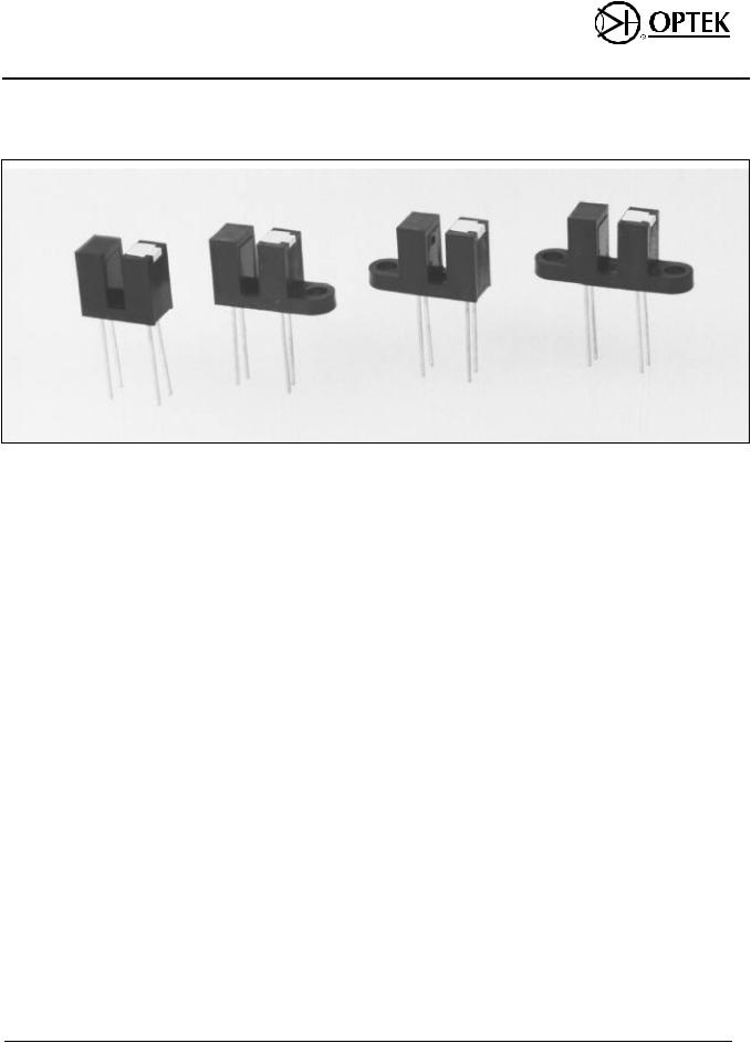
OPTEK OPB360L51, OPB360L11, OPB360L55, OPB360P11, OPB365T51 Datasheet
...
Product Bulletin OPB360
August 1996
Slotted Optical Switches
Types OPB360, OPB370 Series
Package N |
Package L |
Package P |
Package T |
Features |
Absolute Maximum Ratings (TA = 25o C unless otherwise noted) |
||
∙0.125" (3.18 mm) wide gap
∙Choice of aperture
∙Choice of opaque or IR transmissive shell material
∙Choice of mounting configuration
∙Choice of lead spacing
Storage and Operating Temperature Range . . . . . . . . . . . . . . . . . . . . . . . . |
-40o C to +85o C |
Lead Soldering Temperature Range [1/16 inch (1.6 mm) from case for 5 sec. with |
|
soldering iron] . . . . . . . . . . . . . . . . . . . . . . . . . . . . . . . . . . . . . . . . . . . |
. . . . . 240o C(2) |
Input Diode
Forward DC Current . . . . . . . . . . . . . . . . . . . . . . . . . . . . . . . . . . . . . . . . . . . . . 50 mA Peak Forward Current (1 μs pulse width, 300 pps) . . . . . . . . . . . . . . . . . . . . . . . 3.0 A
Reverse DC Voltage . . . . . . . . . . . . . . . . . . . . . . . . . . . . . . . . . . . . . . . . . . . . . . . 2.0 V Power Dissipation . . . . . . . . . . . . . . . . . . . . . . . . . . . . . . . . . . . . . . . . . . . . 100 mW(1)
Description
The OPB360/370 series of slotted switches provides the design engineer with the flexibility of a custom device from a standard product line. Building from a standard housing with a .125" (3.18 mm) wide slot, the user can specify
(1) electrical output parameters, (2) mounting tab configuration, (3) choice of lead spacing, (4) discrete shell material, and (5) aperture width.
All housings are an opaque grade of injection-molded plastic to minimize the assembly's sensitivity to ambient radiation, both visible and near-infrared. Discrete shells (exposed on the parallel faces inside the device throat) are either IR transmissive plastic for applications where aperture contamination may occur or opaque plastic with aperture openings for maximum protection against ambient light.
Output Phototransistor
Collector-EmitterVoltage . . . . . . . . . . . . . . . . . . . . . . . . . . . . . . . . . . . . . . . . . . . . 30 V
Emitter-CollectorVoltage . . . . . . . . . . . . . . . . . . . . . . . . . . . . . . . . . . . . . . . . . . . 5.0 V
Collector DC Current . . . . . . . . . . . . . . . . . . . . . . . . . . . . . . . . . . . . . . . . . . . . . 30 mA
Power Dissipation . . . . . . . . . . . . . . . . . . . . . . . . . . . . . . . . . . . . . . . . . . . . 100 mW(1)
Notes:
(1)Derate linearly 1.67 mW/ o C above 25o C.
(2)RMA flux is recommended. Duration can be extended to 10 sec. max. when flow soldering.
(3)All parameters tested using pulse technique.
(4)Lead spacing of 0.220" (5.59 mm) or 0.320" (8.13 mm) is available. Leads are 0.20" sq. (5.08 mm) and 0.425" (10.80 mm) long (min).
(5)Methanol and isopropanol are recommended as cleaning agents. Plastic housings are soluble in chlorinated hydrocarbons and ketones.
(6)Polarity is denoted by color of housing top:
LED - Gray or Clear
Sensor - Black
Replaces/Upgrades
OPB860, OPB870 Series
Optek Technology, Inc. |
1215W. Crosby Road |
Carollton, Texas 75006 |
(97 2) 323-2200 |
Fax (972) 323-2396 |
12-8

Types OPB360, OPB370 Series
Electrical Characteristics (TA = 25o C unless otherwise noted)
SYMBOL |
PARAMETER |
Input Diode |
|
VF |
Forward Voltage |
IR |
Reverse Current |
Output Phototransistor |
|
V(BR)CEO |
Collector-Emitter Breakdown Voltage |
V(BR)ECO |
Emitter-Collector Breakdown Voltage |
ICEO |
Collector-Emitter Dark Curreent |
Coupled |
|
|
On-State Collector Current |
|
OPB360T, N, L, P55 |
|
OPB365T, N, L, P55 |
|
OPB370T, N, L, P55 |
|
OPB375T, N, L, P55 |
IC(ON) |
OPB360T, N, L, P51 |
OPB365T, N, L, P51 |
|
|
OPB370T, N, L, P51 |
|
OPB375T, N, L, P51 |
OPB360T, N, L, P11
OPB365T, N, L, P11
OPB370T, N, L, P11
OPB375T, N, L, P11
MIN MAX UNITS |
TEST CONDITIONS |
1.7 |
V |
IF = 20 mA |
100 |
μA |
VR = 2 V |
30 |
V |
IC = 1 mA |
5.0V IE = 100 μA
100 |
nA VCE = 10 V, IF = 0, Ee = 0 |
3.5 |
14.0 |
mA |
VCE = 0.4 V, IF = 20 mA |
2.5 |
10.0 |
mA |
VCE = 0.4 V, IF = 20 mA |
1.0 |
5.0 |
mA |
VCE = 0.4 V, IF = 20 mA |
|
PART NUMBER GUIDE |
|
OPB 3 X X X X X |
Optek Assembly |
Aperture Width In Front |
|
of Sensor |
|
5 = .0.050" 1 = 0.010" |
Phototransistor Output |
Aperture Width In Front |
Family |
of Emitter |
|
5 = 0.050" 1= 0.010" |
Discrete Shell Material |
Mounting Configurations |
Designation |
|
6 - Base Mount IR Transmissive |
T -Both Mounting Tabs |
Plastic Discrete Shell |
N - No Mounting Tabs |
PC Mountable Leads |
L - Single Mounting Tab |
|
Emitter Side |
7 - Base Mount Opaque |
P - Single Mounting Tab |
Plastic Discrete Shell |
Phototransistor Side |
PC Mountable Leads |
|
Lead Space Designator |
|
0 = 0.320”(8.12 mm) Lead Space |
|
5 = 0.220”(5.59 mm) Lead Space |
|
Optek reserves the right to make changes at any time in order to improve design and to supply the best product possible.
Optek Technology, Inc. |
1215 W. Crosby Road |
Carrollton, Texas 75006 |
(97 2) 323-2200 |
Fax (972) 323-2396 |
|
|
12-9 |
|
|
 Loading...