UAA2016
Zero Voltage Switch
Power Controller
The UAA2016 is designed to drive triacs with the Zero Voltage
technique which allows RFI−free power regulation of resistive loads.
Operating directly on the AC power line, its main application is the
precision regulation of electrical heating systems such as panel heaters
or irons.
A built−in digital sawtooth waveform permits proportional
temperature regulation action over a ±1°C band around the set point.
For energy savings there is a programmable temperature reduction
function, and for security a sensor failsafe inhibits output pulses when
the sensor connection is broken. Preset temperature (i.e. defrost)
application is also possible. In applications where high hysteresis is
needed, its value can be adjusted up to 5°C around the set point. All
these features are implemented with a very low external component
count.
Features
• Zero Voltage Switch for Triacs, up to 2.0 kW (MAC212A8)
• Direct AC Line Operation
• Proportional Regulation of Temperature over a 1°C Band
• Programmable Temperature Reduction
• Preset Temperature (i.e. Defrost)
• Sensor Failsafe
• Adjustable Hysteresis
• Low External Component Count
• Pb−Free Packages are Available
http://onsemi.com
ZERO VOLTAGE SWITCH
POWER CONTROLLER
PDIP−8
8
1
8
1
x = A or D
A = Assembly Location
WL, L = Wafer Lot
YY, Y = Year
WW, W = Work Week
G, G = Pb−Free Package
(Note: Microdot may be in either location)
P SUFFIX
CASE 626
SOIC−8
D SUFFIX
CASE 751
MARKING
DIAGRAMS
UAA2016P
AWL
YYWWG
8
2016x
ALYW
G
1
Failsafe
Sense Input
Temperature
Reduction
Hysteresis
Adjust
Voltage
Reference
3
4
2
1
4−Bit DAC
11−Bit Counter
(Sawtooth
Generator)
+
−
+
+
+
1/2
Synchronization
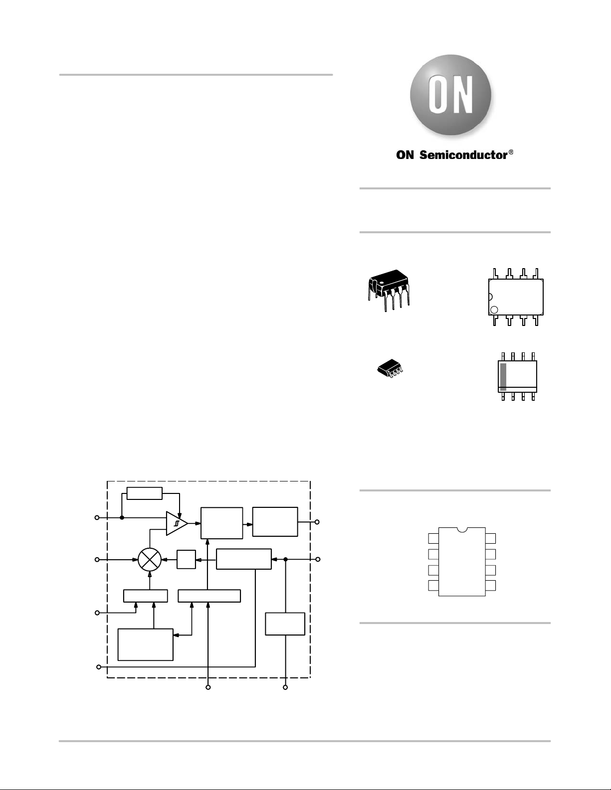
Figure 1. Representative Block Diagram
© Semiconductor Components Industries, LLC, 2006
January, 2006 − Rev. 9
Sampling
Full Wave
Logic
8
Sync
Internal
Reference
UAA2016
Pulse
Amplifier
Supply
Voltage
V
6
Output
7
+V
CC
Temp. Reduc.
PIN CONNECTIONS
V
1
ref
Sensor
2
3
4
(Top View)
Hys. Adj.
Sync
8
V
7
6
Output
V
5
ORDERING INFORMATION
See detailed ordering and shipping information in the package
dimensions section on page 9 of this data sheet.
5
EE
1 Publication Order Number:
UAA2016/D
CC
EE

UAA2016
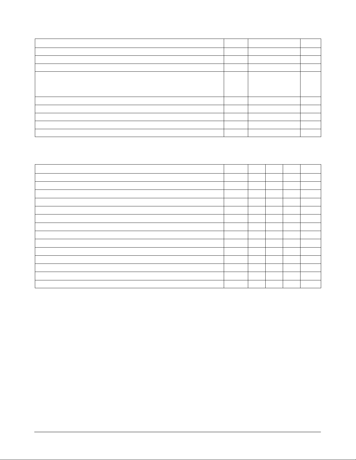
MAXIMUM RATINGS (Voltages referenced to Pin 7)
Rating
Supply Current (I
) I
Pin 5
Non−Repetitive Supply Current, (Pulse Width = 1.0 ms)
AC Synchronization Current I
Pin Voltages V
V
Current Sink I
ref
Output Current (Pin 6), (Pulse Width < 400 ms)
Power Dissipation P
Thermal Resistance, Junction−to−Air
Operating Temperature Range T
Maximum ratings are those values beyond which device damage can occur. Maximum ratings applied to the device are individual stress limit
values (not normal operating conditions) and are not valid simultaneously. If these limits are exceeded, device functional operation is not implied,
damage may occur and reliability may be affected.
ELECTRICAL CHARACTERISTICS (T
= 25°C, VEE = −7.0 V, voltages referred to Pin 7, unless otherwise noted.)
A
Characteristic Symbol Min Typ Max Unit
Supply Current (Pins 6, 8 not connected), (TA = − 20° to + 85°C) I
Stabilized Supply Voltage (Pin 5), (ICC = 2.0 mA) V
Reference Voltage (Pin 1) V
Output Pulse Current (TA = − 20° to + 85°C), (R
Output Leakage Current (V
= 0 V) I
out
Output Pulse Width (TA = − 20° to + 85°C) (Note 1), (Mains = 220 Vrms, R
= 60 W, VEE = − 8.0 V) I
out
= 220 kW)
sync
Comparator Offset (Note 5) V
Sensor Input Bias Current I
Sawtooth Period (Note 2) T
Sawtooth Amplitude (Note 6) A
Temperature Reduction Voltage (Note 3), (Pin 4 Connected to VCC) V
Inter n a l Hysteresis Voltage, (Pin 2 Not Connected) V
Additional Hysteresis (Note 4), (Pin 2 Connected to VCC) V
Failsafe Threshold (TA = − 20° to + 85°C) (Note 7) V
1. Output pulses are centered with respect to zero crossing point. Pulse width is adjusted by the value of R
2. The actual sawtooth period depends on the AC power line frequency. It is exactly 2048 times the corresponding period. For the 50 Hz case
it is 40.96 sec. For the 60 Hz case it is 34.13 sec. This is to comply with the European standard, namely that 2.0 kW loads cannot be connected
or removed from the line more than once every 30 sec. The inertia of most heating systems combined with the UAA2016 will comply with
the European Standard.
3. 350 mV corresponds to 5°C temperature reduction. This is tested at probe using internal test pad. Smaller temperature reduction can be
obtained by adding an external resistor between Pin 4 and VCC. Refer to application curves.
4. 350 mV corresponds to a hysteresis of 5°C. This is tested at probe using internal test pad. Smaller additional hysteresis can be obtained
by adding an external resistor between Pin 2 and VCC. Refer to application curves.
5. Parameter guaranteed but not tested. Worst case 10 mV corresponds to 0.15°C shift on set point.
6. Measured at probe by internal test pad. 70 mV corresponds to 1°C. Note that the proportional band is independent of the NTC value.
7. At very low temperature t he N TC r esistor increases quickly . This c an c ause t he s ensor i nput v oltage t o r each t he f ailsafe t hr eshold, t hus i nhibiting
output pulses; refer to application schematics. The corresponding temperature is the limit at which the circuit works in the typical application.
By setting this threshold at 0.05 V
, the NTC value can increase up to 20 times its nominal value, thus the application works below − 20°C.
ref
Symbol Value Unit
15 mA
200 mA
3.0 mA
0; V
0; V
0; V
0; V
ref
ref
ref
EE
V
1.0 mA
150 mA
625 mW
100 °C/W
− 20 to + 85 °C
− 0.9 1.5 mA
90 100 130 mA
− − 10
50 − 100
− − 0.1
mA
ms
mA
− 40.96 − sec
50 70 90 mV
− 10 − mV
. Refer to application curves.
sync
I
V
V
V
R
CC
CCP
sync
Pin 2
Pin 3
Pin 4
Pin 6
Pin 1
I
O
q
A
CC
EE
ref
O
OL
T
off
IB
TR
IH
FSth
D
JA
−10 −9.0 −8.0 V
−6.5 −5.5 −4.5 V
P
−10 − +10 mV
S
S
280 350 420 mV
280 350 420 mV
H
180 − 300 mV
http://onsemi.com
2

UAA2016
S2
S1
R
S
R
R
def
2
NTC
R
1
Sense Input
Temp. Red.
R
3
3
4
2
Hys
Adj
1
V
ref
Failsafe
++
+
4−Bit DAC
11−Bit Counter
+
−
1/2
Synchronization
Sync
R
sync
Sampling
Full Wave
Logic
Internal
Reference
8
UAA2016
Pulse
Amplifier
Supply
Voltage
V
EE
R
S
MAC212A8
R
6
7
5
Output
+V
C
out
CC
220 Vac
F
Load
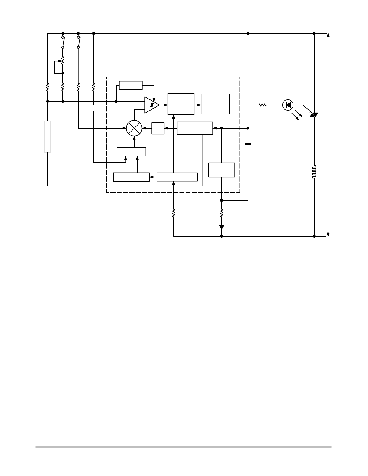
Figure 1. Application Schematic
APPLICATION INFORMATION
(For simplicity, the LED in series with R
is omitted in
out
the following calculations.)
Triac Choice and R
Determination
out
Depending on the power in the load, choose the triac that
has the lowest peak gate trigger current. This will limit the
output current of the UAA2016 and thus its power
consumption. Use Figure 4 to determine R
according to
out
the triac maximum gate current (IGT) and the application
low temperature limit. For a 2.0 kW load at 220 V rms, a good
triac choice is the ON Semiconductor MAC212A8. Its
maximum peak gate trigger current at 25°C is 50 mA.
For an application to work down to − 20°C, R
should be
out
60 W. It is assumed that: IGT(T) = IGT(25°C) exp (−T/125)
with T in °C, which applies to the MAC212A8.
Output Pulse Width, R
The pulse with TP is determined by the triac’s I
sync
Hold
, I
Latch
together with the load value and working conditions
(frequency and voltage):
Given the RMS AC voltage and the load power, the load
value is:
RL = V2rms/POWER
The load current is then:
I
+ (Vrms 2Ǹ sin(2pft)–VTM)ńR
where V
Load
is the maximum on state voltage of the triac, f is
TM
L
the line frequency.
Set I
Load
= I
for t = TP/2 to calculate TP.
Latch
Figures 6 and 7 give the value of TP which corresponds to
the higher of the values of I
VTM= 1.6 V. Figure 8 gives the R
Hold
and I
sync
, assuming that
Latch
that produces the
corresponding TP.
R
and Filter Capacitor
Supply
With the output current and the pulse width determined as
above, use Figures 9 and 10 to determine R
that the sinking current at V
pin (including NTC bridge
ref
Supply
, assuming
current) is less than 0.5 mA. Then use Figure 11 and 12 to
determine the filter capacitor (CF) according to the ripple
desired on supply voltage. The maximum ripple allowed is
1.0 V.
Temperature Reduction Determined by R
1
(Refer to Figures 13 and 14.)
http://onsemi.com
3

UAA2016
Room
Temperature
T (°C)
Heating
Power
P(W)
Proportional Band
Proportional Temperature Control
DReduced Overshoot
DGood Stability
Time (minutes, Typ.)
Overshoot
Time (minutes, Typ.)
Time (minutes, Typ.)Time (minutes, Typ.)
ON/OFF Temperature Control
DLarge Overshoot
DMarginal Stability
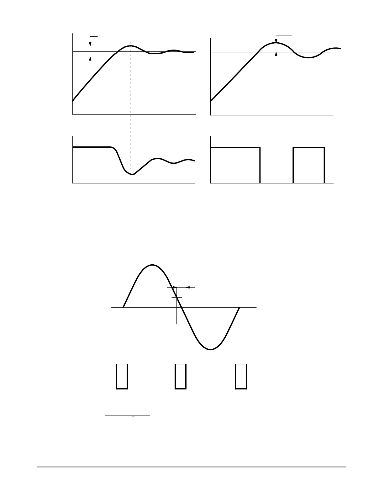
Figure 2. Comparison Between Proportional Control and ON/OFF Control
TP is centered on the zero−crossing.
T
P
AC Line
Waveform
Gate Current
Pulse
14xR
TP+
) 7 10
sync
Ǹ
Vrms 2
xpf
I
Hold
I
Latch
5
(μs)
f = AC Line Frequency (Hz)
Vrms = AC Line RMS Voltage (V)
R
= Synchronization Resistor (W)
sync
Figure 3. Zero Voltage Technique
http://onsemi.com
4

UAA2016
CIRCUIT FUNCTIONAL DESCRIPTION
Power Supply (Pin 5 and Pin 7)
The application uses a current source supplied by a single
high voltage rectifier in series with a power dropping
resistor. An integrated shunt regulator delivers a V
EE
voltage of −8.6 V with respect to Pin 7. The current used by
the total regulating system can be shared in four functional
blocks: IC supply, sensing bridge, triac gate firing pulses and
zener current. The integrated zener, as in any shunt
regulator, absorbs the excess supply current. The 50 Hz
pulsed supply current is smoothed by the large value
capacitor connected between Pins 5 and 7.
Temperature Sensing (Pin 3)
The actual temperature is sensed by a negative
temperature coefficient element connected in a resistor
divider fashion. This two element network is connected
between the ground terminal Pin 5 and the reference voltage
− 5.5 V available on Pin 1. The resulting voltage, a function
of the measured temperature, is applied to Pin 3 and
internally compared to a control voltage whose value
depends on several elements: Sawtooth, Temperature
Reduction and Hysteresis Adjust. (Refer to Application
Information.)
Temperature Reduction
For energy saving, a remotely programmable temperature
reduction is available on Pin 4. The choice of resistor R
connected between Pin 4 and VCC sets the temperature
reduction level.
Comparator
When the noninverting input (Pin 3) receives a voltage
less than the internal reference value, the comparator allows
the triggering logic to deliver pulses to the triac gate. To
improve the noise immunity, the comparator has an
adjustable hysteresis. The external resistor R3 connected to
Pin 2 sets the hysteresis level. Setting Pin 2 open makes a
10 mV hysteresis level, corresponding to 0.15°C. Maximum
hysteresis is obtained by connecting Pin 2 to VCC. In that
case the level is set at 5°C. This configuration can be useful
for low temperature inertia systems.
Sawtooth Generator
In order to comply with European norms, the ON/OFF
period on the load must exceed 30 seconds. This is achieved
by an internal digital sawtooth which performs the
proportional regulation without any additional components.
The sawtooth signal is added to the reference applied to the
comparator inverting input. Figure 2 shows the regulation
improvement using the proportional band action. Figure 4
displays a timing diagram of typical system performance
using the UAA2016. The internal sawtooth generator runs
at a typical 40.96 sec period. The output duty cycle drive
waveform is adjusted depending on the time within the
40.96 sec period the drive needs to turn on. This occurs when
the voltage on the sawtooth waveform is above the voltage
provided at the Sense Input.
Noise Immunity
The noisy environment requires good immunity. Both the
voltage reference and the comparator hysteresis minimize
the noise effect on the comparator input. In addition the
effective triac triggering is enabled every 1/3 sec.
Failsafe
Output pulses are inhibited by the “failsafe” circuit if the
comparator input voltage exceeds the specified threshold
voltage. This would occur if the temperature sensor circuit
is open.
1
Sampling Full Wave Logic
Two consecutive zero−crossing trigger pulses are
generated at every positive mains half−cycle. This ensures
that the number of delivered pulses is even in every case. The
pulse length is selectable by R
connected on Pin 8. The
sync
pulse is centered on the zero−crossing mains waveform.
Pulse Amplifier
The pulse amplifier circuit sinks current pulses from Pin
6 to VEE. The minimum amplitude is 70 mA. The triac is
then triggered in quadrants II and III. The effective output
current amplitude is given by the external resistor R
Eventually, an LED can be inserted in series with the Triac
gate (see Figure 1).
out
.
http://onsemi.com
5

Triac On
Load Voltage
Triac Off
Output Pin
1/2 V
UAA2016
CC
40.96 sec
From Temperature
Sensor (Sense Input)
Figure 4.
200
180
Ω
160
140
120
100
80
out
R , OUTPUT RESISTOR ( )
60
40
TA = +10°C
TA = 0°C
TA = − 20°C
TA = −10°C
20
IGT, TRIAC GATE CURRENT SPECIFIED AT 25°C (mA)
Figure 5. Output Resistor versus
Triac Gate Current
504030 60
100
80
60
40
20
0
Out(min)
I , MINIMUM OUTPUT CURRENT (mA)
TA = + 85°C
TA = − 20°C
R
, OUTPUT RESISTOR (W)
out
Figure 6. Minimum Output Current
versus Output Resistor
200180160140120100806040
http://onsemi.com
6

UAA2016
120
μ
100
80
110 Vrms
60
220 Vrms
40
P
T , OUTPUT PULSE WIDTH ( s)
20
I
Latch(max)
Figure 7. Output Pulse Width versus
400
Ω
300
200
100
F = 50 Hz
2.0 kW Loads
VTM = 1.6 V
TA = 25°C
, MAXIMUM TRIAC LATCH CURRENT (mA)
Maximum Triac Latch Current
220 Vrms
110 Vrms
F = 50 Hz
120
μT , OUTPUT PULSE WIDTH ( s)
100
110 Vrms
80
60
220 Vrms
40
P
6050403020100
20
I
, MAXIMUM TRIAC LATCH CURRENT (mA)
Latch(max)
F = 50 Hz
1.0 kW Loads
VTM = 1.6 V
TA = 25°C
6050403020100
Figure 8. Output Pulse Width versus
Maximum Triac Latch Current
ΩR , MAXIMUM SUPPLY RESISTOR (k )
60
V = 220 Vrms
F = 50 Hz
50
40
30
TP = 50 ms
100 ms
150 ms
sync
0
R , SYNCHRONIZATION RESISTOR (k )
Ω
30
25
20
15
Supply
R , MAXIMUM SUPPLY RESISTOR (k )
10
TP, OUTPUT PULSE WIDTH (ms)
Figure 9. Synchronization Resistor
versus Output Pulse Width
V = 110 Vrms
F = 50 Hz
TP = 50 ms
IO, OUTPUT CURRENT (mA)
Figure 11. Maximum Supply Resistor
versus Output Current
100 ms
150 ms
200 ms
Supply
10080604020
20
IO, OUTPUT CURRENT (mA)
200 ms
1007550250
Figure 10. Maximum Supply
Resistor versus Output Current
90
μ
80
70
60
50
F(min)
40
1007550250
C , MINIMUM FILTER CAPACITOR ( F)
IO, OUTPUT CURRENT (mA)
Ripple = 1.0 Vp−p
F = 50 Hz
200 ms
150 ms
100 ms
TP = 50 ms
100806040200
Figure 12. Minimum Filter Capacitor
versus Output Current
http://onsemi.com
7

UAA2016
3
180
μ
160
140
120
100
F(min)
80
C , MINIMUM FILTER CAPACITOR ( F
6.0
C)
°
5.6
5.2
4.8
4.4
R
T , TEMPERATURE REDUCTION (
4.0
Ripple = 0.5 V
F = 50 Hz
0
IO, OUTPUT CURRENT (mA)
80604020
Figure 13. Minimum Filter Capacitor
versus Output Current
10 kW NTC
100 kW NTC
TS, TEMPERATURE SETPOINT (°C)
Figure 15. Temperature Reduction versus
Temperature Setpoint
200 ms
150 ms
100 ms
TP = 50 ms
R1 = 0
p−p
100
302622181410
7.0
C)
°
6.0
5.0
4.0
3.0
2.0
1.0
R
T , TEMPERATURE REDUCTION (
0
R1, TEMPERATURE REDUCTION RESISTOR (kW)
Figure 14. Temperature Reduction versus R
4
100 kW NTC
3
10 kW NTC
2
1
DEF
R /(NOMINAL NTC VALUE) RATIO
0
T
, PRESET TEMPERATURE (°C)
DEF
Figure 16. R
versus Preset Temperature
DEF
Setpoint = 20°C
10 kW NTC
100 kW NTC
2520151050
1009080706050403020100
1
30
V , COMPARATOR HYSTERESIS VOLTAGE (V)
0.5
0.4
0.3
0.2
0.1
H
0
0
R3, HYSTERESIS ADJUST RESISTOR (kW)
8
6
4
2
S2
R + R /(NOMINAL NTC VALUE) RATIO
(
0
T
10 kW NTC
R
DEF
100 kW NTC
R
= 310 kW
DEF
TS, TEMPERATURE SETPOINT (°C)
= 4°C
DEF
= 29 kW
34302622181410
Figure 17. RS + R2 versus Preset Setpoint Figure 18. Comparator Hysteresis versus R
http://onsemi.com
8
400300200100

UAA2016
ORDERING INFORMATION
Device Operating Temperature Range Package Shipping
UAA2016D
UAA2016DG SOIC−8
UAA2016AD SOIC−8 98 Units / Rail
T
= −20° to +85°C
UAA2016ADG SOIC−8
UAA2016P PDIP−8 1000 Units / Rail
UAA2016PG PDIP−8
†For information on tape and reel specifications, including part orientation and tape sizes, please refer to our Tape and Reel Packaging
Specifications Brochure, BRD8011/D.
A
SOIC−8 98 Units / Rail
98 Units / Rail
(Pb−Free)
98 Units / Rail
(Pb−Free)
1000 Units / Rail
(Pb−Free)
†
http://onsemi.com
9

PDIP−8
NOTE 2
−T−
SEATING
PLANE
H
58
−B−
14
F
−A−
C
N
D
G
0.13 (0.005) B
UAA2016
PACKAGE DIMENSIONS
P SUFFIX
CASE 626−05
ISSUE L
K
M
M
A
T
M
NOTES:
1. DIMENSION L TO CENTER OF LEAD WHEN
FORMED PARALLEL.
2. PACKAGE CONTOUR OPTIONAL (ROUND OR
SQUARE CORNERS).
3. DIMENSIONING AND TOLERANCING PER ANSI
Y14.5M, 1982.
DIM MIN MAX MIN MAX
A 9.40 10.16 0.370 0.400
B 6.10 6.60 0.240 0.260
C 3.94 4.45 0.155 0.175
D 0.38 0.51 0.015 0.020
L
J
F 1.02 1.78 0.040 0.070
G 2.54 BSC 0.100 BSC
H 0.76 1.27 0.030 0.050
J 0.20 0.30 0.008 0.012
K 2.92 3.43 0.115 0.135
L 7.62 BSC 0.300 BSC
M −−− 10 −−− 10
N 0.76 1.01 0.030 0.040
INCHESMILLIMETERS
__
M
http://onsemi.com
10

−Y−
−Z−
UAA2016
PACKAGE DIMENSIONS
SOIC−8
D SUFFIX
CASE 751−07
ISSUE AG
NOTES:
−X−
A
58
B
1
S
0.25 (0.010)
4
M
M
Y
K
G
N
C
SEATING
PLANE
0.10 (0.004)
H
D
0.25 (0.010) Z
M
Y
SXS
X 45
_
M
J
1. DIMENSIONING AND TOLERANCING PER
ANSI Y14.5M, 1982.
2. CONTROLLING DIMENSION: MILLIMETER.
3. DIMENSION A AND B DO NOT INCLUDE
MOLD PROTRUSION.
4. MAXIMUM MOLD PROTRUSION 0.15 (0.006)
PER SIDE.
5. DIMENSION D DOES NOT INCLUDE DAMBAR
PROTRUSION. ALLOWABLE DAMBAR
PROTRUSION SHALL BE 0.127 (0.005) TOTAL
IN EXCESS OF THE D DIMENSION AT
MAXIMUM MATERIAL CONDITION.
6. 751−01 THRU 751−06 ARE OBSOLETE. NEW
STANDARD IS 751−07.
MILLIMETERS
DIMAMIN MAX MIN MAX
4.80 5.00 0.189 0.197
B 3.80 4.00 0.150 0.157
C 1.35 1.75 0.053 0.069
D 0.33 0.51 0.013 0.020
G 1.27 BSC 0.050 BSC
H 0.10 0.25 0.004 0.010
J 0.19 0.25 0.007 0.010
K 0.40 1.27 0.016 0.050
M 0 8 0 8
____
N 0.25 0.50 0.010 0.020
S 5.80 6.20 0.228 0.244
INCHES
SOLDERING FOOTPRINT*
1.52
0.060
7.0
0.275
0.6
0.024
*For additional information on our Pb−Free strategy and soldering
details, please download the ON Semiconductor Soldering and
Mounting Techniques Reference Manual, SOLDERRM/D.
4.0
0.155
1.270
0.050
SCALE 6:1
mm
ǒ
inches
Ǔ
http://onsemi.com
11

UAA2016
ON Semiconductor and are registered trademarks of Semiconductor Components Industries, LLC (SCILLC). SCILLC reserves the right to make changes without further notice
to any products herein. SCILLC makes no warranty, representation or guarantee regarding the suitability of its products for any particular purpose, nor does SCILLC assume any liability
arising out of the application or use of any product or circuit, and specifically disclaims any and all liability, including without limitation special, consequential or incidental damages.
“Typical” parameters which may be provided in SCILLC data sheets and/or specifications can and do vary in different applications and actual performance may vary over time. All
operating parameters, including “Typicals” must be validated for each customer application by customer’s technical experts. SCILLC does not convey any license under its patent rights
nor the rights of others. SCILLC products are not designed, intended, or authorized for use as components in systems intended for surgical implant into the body, or other applications
intended to support or sustain life, or for any other application in which the failure of the SCILLC product could create a situation where personal injury or death may occur. Should
Buyer purchase or use SCILLC products for any such unintended or unauthorized application, Buyer shall indemnify and hold SCILLC and its officers, employees, subsidiaries, affiliates,
and distributors harmless against all claims, costs, damages, and expenses, and reasonable attorney fees arising out of, directly or indirectly, any claim of personal injury or death
associated with such unintended or unauthorized use, even if such claim alleges that SCILLC was negligent regarding the design or manufacture of the part. SCILLC is an Equal
Opportunity/Affirmative Action Employer. This literature is subject to all applicable copyright laws and is not for resale in any manner.
PUBLICATION ORDERING INFORMATION
LITERATURE FULFILLMENT:
Literature Distribution Center for ON Semiconductor
P.O. Box 61312, Phoenix, Arizona 85082−1312 USA
Phone: 480−829−7710 or 800−344−3860 Toll Free USA/Canada
Fax: 480−829−7709 or 800−344−3867 Toll Free USA/Canada
Email: orderlit@onsemi.com
N. American Technical Support: 800−282−9855 Toll Free
USA/Canada
Japan: ON Semiconductor, Japan Customer Focus Center
2−9−1 Kamimeguro, Meguro−ku, Tokyo, Japan 153−0051
Phone: 81−3−5773−3850
http://onsemi.com
ON Semiconductor Website: http://onsemi.com
Order Literature: http://www.onsemi.com/litorder
For additional information, please contact your
local Sales Representative.
UAA2016/D
12
 Loading...